
 Open Access Article
 This Open Access Article is licensed under a
 Creative Commons Attribution 3.0 Unported Licence
Antimonene: a monolayer material for ultraviolet optical nanodevices†
Deobrat
Singh
a,
Sanjeev K.
Gupta
*b,
Yogesh
Sonvane
a and
Igor
Lukačević
*c
aDepartment of Applied Physics, S. V. National Institute of Technology, Surat, 395007, India
bDepartment of Physics and Electronics, St. Xavier's College, Ahmedabad, 380009, India. E-mail: sanjeev.gupta@sxca.edu.in
cDepartment of Physics, University J. J. Strossmayer, 31000 Osijek, Croatia. E-mail: ilukacevic@fizika.unios.hr
First published on 10th June 2016
Abstract
Two-dimensional materials draw further attention because of their superior properties applicable in novel technologies. We have calculated the optical properties of α and β allotropes of antimonene monolayers. Their dielectric matrices have been calculated within the random phase approximation (RPA) using density functional theory. We have calculated dielectric functions, absorption coefficients, refractive indices, electron energy loss spectra and optical reflectivities in the energy range between 0 and 21 eV. Our simulations predict that absorption process starts in the infrared, but peaks in the ultraviolet region. The values of refractive index are 2.3 (α-Sb) and 1.5 (β-Sb) at the zero energy limit and scale up to 3.6 in the ultraviolet region. Reflection rises up to 86% at the UV energies, where antimonene behaves like a metal regarding the incident electromagnetic radiation. Our calculations show that antimonene is suitable as a material for the microelectronic and optoelectronic nanodevices and solar cell applications, as well as for new optical applications using various light emission, detection, modulation and manipulation functions.
A Introduction
Two-dimensional (2D) materials, including graphene, MoS2 and elemental monolayers, are being proposed as next generation materials for future technologies via manipulation of their electronic and optical properties. This has led to the characterization of these 2D materials using the spectroscopic techniques together with theoretical calculations. For example, the optical reflectivity of graphene in the spectral range of 0.2–1.2 eV was calculated.1 Nonlinear optical edge states of MoS2 were used for the all-optical determination of its crystal orientations.2 The optical absorption and photoluminescence of MoS2 were reported to increase with decreasing electric gate voltage.3 For the graphitic GaN sheet, the static dielectric constant and refractive index were calculated.4 Spectroscopic ellipsometry measurements were also performed to characterize the complex refractive index of monolayer transition metal dichalcogenides (MX2; M = Mo, W; X = S, Se).5Very recently, antimonene (Sb), a layered material consisting of sheets of sp3-hybridized antimony atoms puckered along the so-called in-plane armchair direction and held together by weak van der Waals forces was predicted to be stable.6–8 Regarding its beneficial electronic properties, it will be, from the experimental point of view, interesting to grow antimonene by the isolation of the few-layer forms of antimonene for spectroscopic and electrical characterization. Like other ultrathin 2D crystals, it also allows for superior electrostatic modulation of the carrier density, a feature that is necessary for continuous nanoscale transistor scaling.9–13 Although antimonene has not been experimentally verified until now, there are many intriguing properties, obtainable through ab initio simulations, which require the attention of scientific community. The rising interest in antimonene in photonics and optoelectronics is supported by the numerous applications of similar monolayer materials ranging from solar cells and light-emitting devices to touch screens, photo-detectors and ultrafast lasers.14–17
In this paper, the optical properties of antimonene are investigated with an aim to get insight into the occupied and unoccupied electronic bands as well as the knowledge about the band characteristics. Our motivation is to characterize antimonene as one of the promising optoelectronic and nanophotonic materials, whose optical properties are coupled to its beneficiary two-dimensional morphology. The paper is organized in four sections. Section B describes the methodology and the theoretical formulation employed in the calculations. In Section C, the relevant density of states, refractive indices and other optical properties of antimonene (Sb) are discussed. Finally, short concluding remarks are presented in Section D.
B Computational details
Calculations based on density functional theory (DFT) were performed using the Vienna ab-initio Simulation Package (VASP).18–20 The plane wave basis set with the projector augmented wave (PAW) pseudopotential approach was used to model the interactions between valence electrons and ionic cores. The exchange–correlation potentials were approximated by the generalized gradient approximation (GGA) functional as parameterized by Perdew, Burke and Ernzerhof (PBE)21 and the screened hybrid functional (HSE06),22 with spin orbit coupling (SOC) terms included. In the self-consistent field potential and total energy calculations of the structural and the optical properties, k-point sampling was set to be (22 × 22 × 1) and (15 × 15 × 1) for the α-Sb and β-Sb, respectively. To calculate the electronic band structure with the HSE06, we used (5 × 5 × 1) k-point mesh. The kinetic energy cut-off for the plane wave basis set was taken to be 500 eV. All the atoms in the unit cell are fully relaxed until the force on each atom was below the 0.001 eV Å−1 and the convergence criteria for energy in the self-consistent field cycle was taken to be 1 × 10⁻⁶ eV. The supercell is periodic in the XY-plane and is separated by 20 Å slab along the z-direction to avoid the interaction between adjacent planes.To calculate the optical properties including dielectric function, refractive index, absorbance, reflectance and electron energy loss spectra (EELS), DFT within the random phase approximation (RPA) was used.23 The dielectric function can be written as ε(ω) = ε1(ω) + iε2(ω). Here ε1(ω) and ε2(ω) are the real and imaginary parts of the complex dielectric function, respectively. ε2(ω) is determined by summation over electronic states and ε1(ω) is obtained using the Kramers–Kronig relationship.23–26 Note that the c axis was taken to be normal to the plane of 2D sheet.
If we assume orientation of the crystal surface perpendicular to the optical axis, the reflectivity R(ω) follows directly from Fresnel's formula,
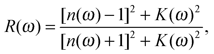 | (1) |
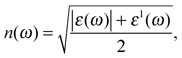
 | (2) |
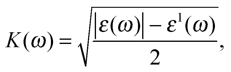 | (3) |
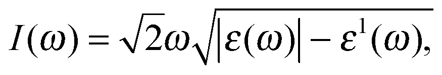
 | (4) |
 | (5) |
 is the relative dielectric constant.
C Results and discussion
Fig. 1 shows the structural configurations of the puckered α-Sb and buckled β-Sb obtained at the PBE-DFT level of theory. The α-Sb has a puckered atomic structure and it contains four atoms per unit cell with two sublayers, where atoms positioned in the same sublayer are not in the same plane (Fig. 1 (α-Sb)). The α-Sb structure is arranged in a rectangular lattice with a puckered surface, while the ground-state configuration of β-Sb has a buckled atomic structure like a hexagon, but not planar (Fig. 1 (β-Sb)), with two atoms per unit cell.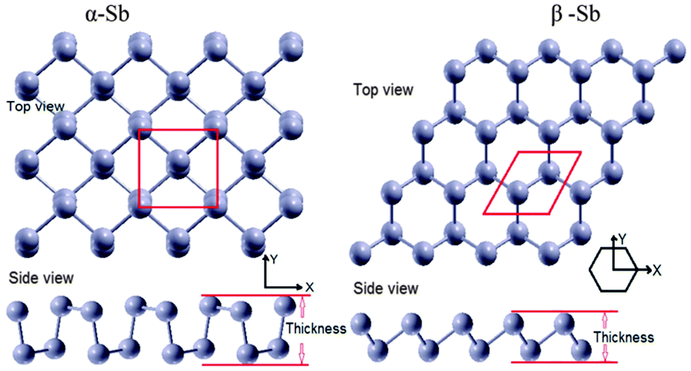 | ||
| Fig. 1 Structural configurations of two stable allotropes of antimony α and β phase. | ||
Electronic density of states
Electronic properties are obtained using both PBE and HSE06 functionals (see Fig. S1, ESI†). The calculated total density of states (TDOS) and partial density of states (PDOS) for α-Sb and β-Sb are displayed in Fig. 2 showing three sub-bands: (i) the lower valence bands (<−6 eV (α-Sb), <−7.50 eV (β-Sb)), essentially dominated by 5s states; (ii) the sub-bands dominated by 5p states near the Fermi level; and (iii) the hybridized p–d sub-bands (>0 eV). Small band gap of less than 1.2 eV indicates that antimonene will not be optically transparent, as there will be an appreciable amount of free carriers created by absorption even at room temperature.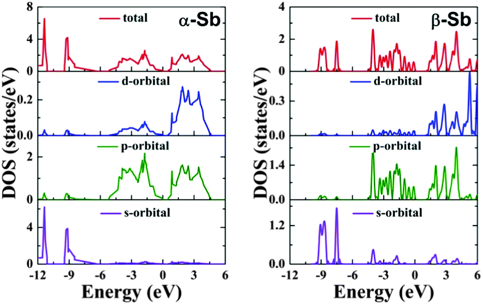 | ||
| Fig. 2 Total and partial density of states of α-Sb (left) and β-Sb (right) monolayers obtained using hybrid functional HSE06. | ||
Optical properties
Fig. 3 shows the real and imaginary parts of the complex dielectric functions, ε(ω) (see, also, Fig. S2, ESI†). The distinct features in ε2(ω) are related to the interband transitions corresponding to the absorption of radiation by electrons in occupied valence bands below the Fermi level. On the other hand, ε1(ω) tells us about the electronic polarizability of the material through the Clausius–Mossotti relation. Other polarizability contributions (ionic and dipolar) can be neglected in the studied energy range because of the inertia of the atomic cores and molecules.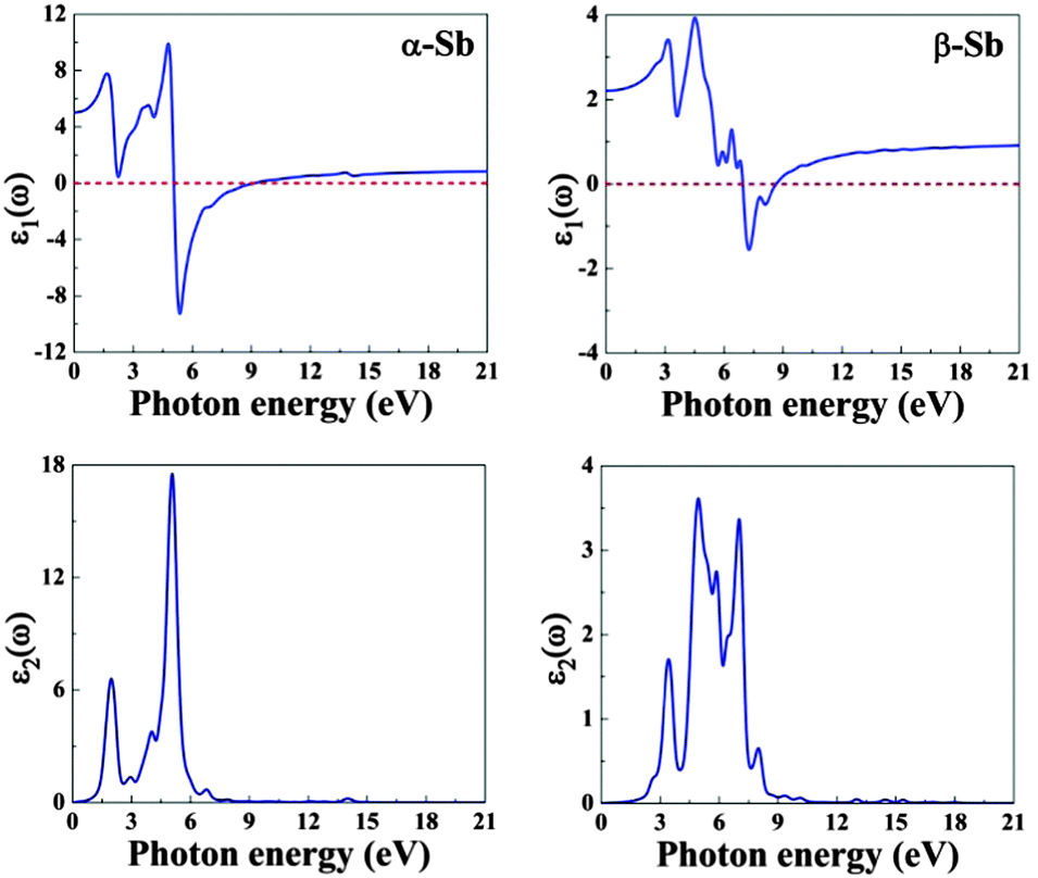 | ||
| Fig. 3 The real and imaginary parts of complex dielectric function of α-Sb (left) and β-Sb (right) monolayers obtained using hybrid functional HSE06. | ||
The calculated static dielectric constant (dielectric constant at the zero frequency limit) is 5.1 and 2.2 for α-Sb and β-Sb, respectively, suggesting α-Sb to have relatively high polarizability. In the real part of dielectric function, negative values occur in the ranges between 5.0 eV and 9.0 eV (α-Sb) and between 6.9 eV and 8.4 eV (β-Sb). This indicates the metallic character of α-Sb and β-Sb in the UV part of the electromagnetic spectrum.
In the imaginary part of the dielectric function ε(ω), there are several peaks: at 1.9 eV, 4.0 eV, 5.0 eV and 6.6 eV for α-Sb; and at 3.4 eV, 4.7 eV, 5.9 eV, 6.9 eV and 8.0 eV for β-Sb. For α-Sb, all four peaks in the imaginary part of dielectric function are mainly due to the electronic transitions from 5p states in the valence band to hybridized orbitals 5p/4d in the conduction band. In the case of β-Sb, the first four peaks are mainly due to the electronic transitions from 5p states to hybridized 5p/4d or pure 4d orbitals, while the last peak (8.0 eV) can be due to the electronic transitions from 5p to pure 4d orbitals or from 5s to hybridized 5p/4d orbitals.
The contribution to the dielectric function of direct and indirect interband transitions dominated by absorption from the valence band maximum to the conduction band minimum is small (energies up to 1.2 eV in Fig. 3). Contrary to that, electronic band structures show large regions of “tracking” bands, the regions where the energy difference between the valence and conduction bands is approximately the same (Fig. 4).
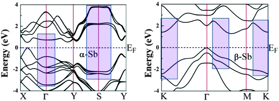 | ||
| Fig. 4 Electronic band structure of α-Sb (left) and β-Sb (right) obtained using hybrid functional HSE06. “Tracking” band regions (shaded areas) are seen in both allotropes: around S and gamma (α-Sb) and around K and between gamma and M points (β-Sb). | ||
In α-Sb, these regions include the portions of the Brillouin zone around the S point and somewhat less around the gamma point. In β-Sb “tracking” bands are found around the K point and between the gamma and M points. Around these joint critical points energy difference has a small gradient producing, thus, large contributions to the electronic density of states. Large density of states enables higher transition probabilities, which in turn give rise to distinct structures in the dielectric function (Fig. 3), i.e. they have strong contributions to the optical properties.
The fundamental gaps of 0.54 eV and 1.18 eV for α-Sb and β-Sb, respectively, are in agreement with the previous DFT calculations and follow the trend of improving the band gap value over the PBE or LDA functional.7 It is well known that materials with band gaps below the 1.65 eV absorb well in the infrared (IR) region of the spectrum. Therefore, antimonene will start to absorb electromagnetic radiation in the IR region as an optical material. Since the imaginary part of the dielectric function is related to the absorption, it is clear from Fig. 3 that, although antimonene's absorption edge appears in the IR, its absorptivity will not peak in IR, but in a region 2–5 eV for α-Sb and 3–7 eV for β-Sb.
The optical constants of antimonene, refractive index n(ω) and extinction coefficient K(ω) are represented in Fig. 5. The static refractive index n(0) is 2.3 and 1.5 for α-Sb and β-Sb, respectively. In α-Sb the refractive index n(ω) increases with energy in the IR region, while in the UV region it steadily decreases. In β-Sb it increases monotonically even into near UV, where after oscillations it decreases into far UV. The maximum refractive index is 3.6 at 4.8 eV and 2.0 at 4.3 eV for α-Sb and β-Sb monolayers, respectively. These high refractive indices could enable antimonene to be used as an inner layer coating between the UV absorbing layer and the substrate.
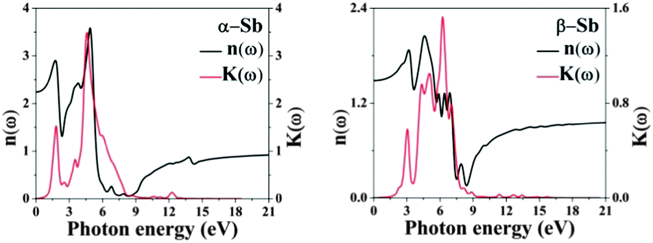 | ||
| Fig. 5 The refractive index n(ω) and extinction coefficient K(ω) of α-Sb and β-Sb monolayers obtained using hybrid functional HSE06. | ||
The spectrum curves of the extinction coefficient K(ω) of both phases, α-Sb and β-Sb, rapidly decrease with increasing photon energy in the UV region and become constant after 16 eV. The maxima obtained in the extinction coefficient are at 5.4 eV for α-Sb and at 5.6 eV for the β-Sb monolayer. At these energies the photons will be absorbed very fast, i.e. their depth path will be the shortest. Decay length, δ = c/ωK, a quantity analogous to the skin depth relating to an alternating current passing through a conductor, tells us the distance at which the wave intensity will fall down to 1/e of its surface value. For α-Sb this length would be 14 nm (140 Å), while for β-Sb it would be 17 nm (170 Å), which is much greater than the thickness of monolayers: 3.2 Å (α-Sb) and 1.6 Å (β-Sb), and, thus, does not play a significant role in antimonene as a monolayer material.
The absorption coefficient I(ω) of α-Sb and β-Sb is shown in Fig. 6 (see Fig. 3, ESI† for the comparison of different functionals). The absorption coefficient describes the decay of light intensity which traverses through the unit distance in a medium. The calculated absorption coefficient for both allotropes is zero when the energy is below 2.0 eV (α-Sb) and 0.59 eV (β-Sb). Thereafter, the absorption coefficient increases, indicating that the absorption processes can occur at the corresponding photon energies. There are many peaks within the studied energy range whose structure can be explained by the interband transitions using partial and total density of state, similarly to the discussion about the dielectric function. As stated above, at small energies the absorption spectra have low intensity, since there are not a lot of electronic states which play a role as initial states in the absorption processes. On the other hand, absorption spectra reach their maxima at about 5.3 eV (α-Sb) and 7.1 eV (β-Sb). The first peak in the absorption spectrum of α-Sb occurs at 2.1 eV and most probably corresponds to the direct electronic transition at the k-point between the gamma and Y points. The other peaks occur at 4.0 eV, 5.3 eV and 6.7 eV. The maximal peak at 5.3 eV most probably corresponds to the transitions from the top valence band to the conduction bands in a broad region of the Brillouin zone around the S point. In the case of β-Sb, first peak in the absorption spectrum occurs at 3.2 eV and the other peaks occur at 5.0 eV, 5.9 eV, 7.1 eV and 8.0 eV. The maximal peak at 7.1 eV is most probably due to the transitions occurring around the K point in the Brillouin zone. These results confirm the conclusion obtained from the analyses of dielectric functions, that the absorption in antimonene will be the strongest in the UV part of electromagnetic spectrum.
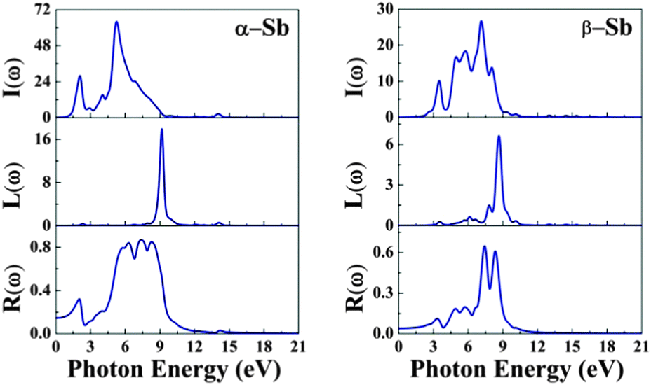 | ||
| Fig. 6 The absorption coefficient I(ω), energy loss spectrum L(ω) and reflectivity R(ω) of α-Sb (left) and β-Sb (right) monolayers obtained using hybrid functional HSE06. The unit of absorption coefficient is 105/cm. | ||
We can optimize different properties of materials by the contribution from the energy loss spectrum L(ω) (EELS). There are several ways for exciting electrons in a medium other than by absorption of photons. When a fast electron travels in a solid medium it may lose some energy, represented by L(ω), and excite other electrons in the solid. In the case of intra- and interband transitions, plasmon excitations can be identified by analyzing the L(ω) spectrum, which is related to the dielectric function by eqn (5). The highest peaks in L(ω) spectra represent the characteristics associated with the plasma resonance and the corresponding frequency is known as plasma frequency.25,26 If the incident electromagnetic radiation has a frequency which is lower than the plasma frequency of antimonene, the plasma oscillations will successfully screen the electric field. This will result in reflection of the incident radiation from the surface of the material and an increase in reflection intensity, like in metals. Thus, the peaks in L(ω) also correspond to the trailing edges in the reflection spectra.25,26 There is only one significant peak associated with both allotropes: for α-Sb the one at 9.1 eV, while for β-Sb, the one at 8.7 eV; corresponding to the abrupt reduction in reflectivity R(ω) at the same energy. These peaks correspond to and agree with the energies at which the real part of the dielectric function is negative (9.0 eV and 8.4 eV in Fig. 2). If the radiation frequency is higher than the plasma frequency, plasma oscillations cannot follow the oscillations in the electric field, the reflectivity R(ω) vanishes, and the electromagnetic wave can enter the material and propagate experiencing the losses described by the absorption (I(ω)) and EELS (L(ω)) spectra.
It can be noticed (Fig. 6) that there are several peaks in the reflectivity curves up to 16 eV. The maximum reflectivity reaches the large values of 86% and 64% for α-Sb and β-Sb, respectively, and maximum peaks occur at 7.3 eV for both allotropes. The specific profiles of reflectance spectra – prominent peaks occurring at different parts of the UV spectrum – could allow the usage of antimonene in selective UV mirrors. This is particularly emphasized in β-Sb, where the reflectivity does not exceed 20% up to far UV and in the far UV it increases by about three times. Furthermore, low absorption in the IR part of the spectrum means that antimonene will not absorb heat and could act as a sort of cold mirror material in applications like beam splitters or in optical fibers in combination with hot mirrors.
D Conclusions
Density functional theory (DFT) within the random phase approximation (RPA) predicts interesting optical properties of 2D antimonene monolayers with puckered (α-Sb) and buckled (β-Sb) structures. Applications of antimonene as an optic material rise from its specific dielectric function, absorption, reflectivity, refractivity and energy loss spectra. In both allotropes, a high refractive index of up to 3.6 is found in the UV part of the electromagnetic spectrum allowing applications as an inner layer coating under UV absorbers. The dielectric function and electron loss spectra (EELS) reveal the plasmon energies of around 9 eV and, thus, the parts of the electromagnetic spectrum where antimonene behaves like a metal regarding the reflection of light. Although the absorption process starts in the IR part of the spectrum, it peaks in the UV part having a steady fall toward the high energy UV. Our conjecture is that the optical properties of antimonene could be further modified by strain engineering or doping methods toward more specific application designs. Our theoretical simulations suggest further experimental investigations, which could lead to applications of antimonene in the field of photonics where absorption in the ultraviolet region is required and it may provide a new material which has possibilities to be applied in microelectronic and optoelectronic devices and solar cells.Acknowledgements
K2, high performance computing clusters at IUAC, New Delhi, was used in obtaining results presented in this paper. Helpful discussions with Prof. Ravindra Pandey and Gaoxue Wang are gratefully acknowledged. IL and SKG would like to acknowledge the financial support through the project “Multifunctional materials – properties and applications” funded by the University J. J. Strossmayer in Osijek, Croatia.References
- K. F. Mak, M. Y. Sfeir, Y. Wu, C. H. Lui, J. A. Misewich, T. F. Heinz and L. A. Falkovsky, J. Phys.: Conf. Ser., 2008, 129, 012004 CrossRef.
- X. Yin, Z. Ye, D. A. Chenet, Y. Ye, K. O'Brien, J. C. Hone and X. Zhang, Science, 2014, 344, 488 CrossRef CAS PubMed.
- A. K. M. Newaz, D. Prasai, J. I. Ziegler, D. Caudel, S. Robinson, R. F. Haglun Jr. and K. I. Bolotin, Solid State Commun., 2013, 155, 49 CrossRef CAS.
- S. Behzad, J. Mater. Sci.: Mater. Electron., 2015, 26, 9898 CrossRef CAS.
- H. L. Liu, C. C. Shen, S. H. Su, C. L. Hsu, M. Y. Li and L. J. Li, Appl. Phys. Lett., 2014, 105, 201905 CrossRef.
- G. Wang, R. Pandey and S. P. Karna, ACS Appl. Mater. Interfaces, 2015, 7, 11490 Search PubMed.
- O. Üzengi Aktürk, V. Ongun Özçelik and S. Ciraci, Phys. Rev. B: Condens. Matter Mater. Phys., 2015, 91, 235446 CrossRef.
- S. Zhang, Z. Yan, Y. Li, Z. Chen and H. Zeng, Angew. Chem., Int. Ed., 2015, 127, 1 CrossRef.
- B. Amin, N. Singh and U. Schwingenschlögl, Phys. Rev. B: Condens. Matter Mater. Phys., 2015, 92, 075439 CrossRef.
- Y. Zhao, Y. Zhang, Z. Yang, Y. Yan and K. Sun, Sci. Technol. Adv. Mater., 2013, 14, 043501 CrossRef PubMed.
- D. J. Late, Y.-K. Huang, B. Liu, J. Acharya, S. N. Shirodkar, J. Luo, A. Yan, D. Charles, U. V. Waghmare, V. P. Dravid and C. N. Rao, ACS Nano, 2013, 7, 4879 CrossRef CAS PubMed.
- Y. Li, H. Wang, L. Xie, Y. Liang, G. Hong and H. Dai, J. Am. Chem. Soc., 2011, 133, 7296 CrossRef CAS PubMed.
- M. Chhowalla, H. S. Shin, G. Eda, L.-J. Li, K. P. Loh and H. Zhang, Nat. Chem., 2013, 5, 263 CrossRef PubMed.
- F. Bonaccorso, Z. Sun, T. Hasan and A. C. Ferrari, Nat. Photonics, 2010, 4, 611 CrossRef CAS.
- C. Ingrosso, G. V. Bianco, M. Corricelli, R. Comparelli, D. Altamura, A. Agostiano, M. Striccoli, M. Losurdo, M. L. Curri and G. Bruno, ACS Appl. Mater. Interfaces, 2015, 7, 4151 CAS.
- R. Cheng, D. Li, H. Zhou, C. Wang, A. Yin, S. Jiang, Y. Liu, Y. Chen, Y. Huang and X. Duan, Nano Lett., 2014, 14, 5590 CrossRef CAS PubMed.
- A. Beltaos, A. Kovačević, A. Matković, U. Ralević, D. Jovanović and B. Jelenković, Phys. Scr., 2014, 162, 014015 CrossRef.
- G. Kresse and J. Furthmüller, Phys. Rev. B: Condens. Matter Mater. Phys., 1996, 54, 11169 CrossRef CAS.
- G. Kresse and D. Joubert, Phys. Rev. B: Condens. Matter Mater. Phys., 1999, 59, 1758 CrossRef CAS.
- W. Kohn and L. J. Sham, Phys. Rev. A: At., Mol., Opt. Phys., 1965, 140, 1133 Search PubMed.
- J. P. Perdew, K. Burke and M. Ernzerhof, Phys. Rev. Lett., 1996, 77, 3865 CrossRef CAS PubMed.
- J. Heyd, G. E. Scuseria and M. Ernzerhof, J. Chem. Phys., 2006, 124, 219906 CrossRef.
- M. Gajdoš, K. Hummer, G. Kresse, J. Furthmüller and F. Bechstedt, Phys. Rev. B: Condens. Matter Mater. Phys., 2006, 73, 045112 CrossRef.
- C. Ambrosch-Draxl and J. O. Sofo, Comput. Phys. Commun., 2006, 175, 1 CrossRef CAS.
- M. Fox, Optical Properties of Solids, Oxford University Press, New York, 2001, vol. 3 Search PubMed.
- F. Wooten, Properties of Solids, Academic Press, New York, 1972 Search PubMed.
Footnote |
| † Electronic supplementary information (ESI) available. See DOI: 10.1039/c6tc01913g |
| This journal is © The Royal Society of Chemistry 2016 |