
 Open Access Article
 This Open Access Article is licensed under a
 Creative Commons Attribution 3.0 Unported Licence
Controlling mixed conductivity in Na1/2Bi1/2TiO3 using A-site non-stoichiometry and Nb-donor doping
Linhao
Li
 a,
Ming
Li
b,
Huairuo
Zhang
a,
Ian M.
Reaney
a and
Derek C.
Sinclair
*a
a,
Ming
Li
b,
Huairuo
Zhang
a,
Ian M.
Reaney
a and
Derek C.
Sinclair
*a
aSir Robert Hadfield Building, Department of Materials Science & Engineering, Mappin Street, University of Sheffield, Sheffield, S1 3JD, UK. E-mail: d.c.sinclair@sheffield.ac.uk
bDepartment of Mechanical, Materials and Manufacturing Engineering, University of Nottingham, University Park, Nottingham, NG7 2RD, UK
First published on 20th May 2016
Abstract
Precise control of electronic and/or ionic conductivity in electroceramics is crucial to achieve the desired functional properties as well as to improve manufacturing practices. We recently reported the conventional piezoelectric material Na1/2Bi1/2TiO3 (NBT) can be tuned into a novel oxide-ion conductor with an oxide-ion transport number (tion) > 0.9 by creating bismuth and oxygen vacancies. A small Bi-excess in the nominal starting composition (Na0.50Bi0.50+xTiO3+3x/2, x = 0.01) or Nb-donor doping (Na0.50Bi0.50Ti1−yNbyO3+y/2, 0.005 ≤ y ≤ 0.030) can reduce significantly the electrical conductivity to create dielectric behaviour by filling oxygen vacancies and suppressing oxide ion conduction (tion ≤ 0.10). Here we show a further increase in the starting Bi-excess content (0.02 ≤ x ≤ 0.10) reintroduces significant levels of oxide-ion conductivity and increases tion ∼ 0.4–0.6 to create mixed ionic/electronic behaviour. The switch from insulating to mixed conducting behaviour for x > 0.01 is linked to the presence of Bi-rich secondary phases and we discuss possible explanations for this effect. Mixed conducting behaviour with tion ∼ 0.5–0.6 can also be achieved with lower levels of Nb-doping (y ∼ 0.003) due to incomplete filling of oxygen vacancies without the presence of secondary phases. NBT can now be compositionally tailored to exhibit three types of electrical behaviour; Type I (oxide-ion conductor); Type II (mixed ionic-electronic conductor); Type III (insulator) and these results reveal an approach to fine-tune tion in NBT from near unity to zero. In addition to developing new oxide-ion and now mixed ionic/electronic NBT-based conductors, this flexibility in control of oxygen vacancies allows fine-tuning of both the dielectric/piezoelectric properties and design manufacturing practices for NBT-based multilayer piezoelectric devices.
Introduction
It has been long known that low levels of non-stoichiometry in functional oxides, either associated with intentional element doping or unintentional element loss/gain during processing or impurities in raw materials can induce significant changes in functional properties.1–3 Understanding the defect chemistry and controlling non-stoichiometry in functional oxides is a powerful and proven approach to improve the desired electronic, ionic, mixed ionic/electronic and/or polar dielectric properties of existing materials, design new materials and optimise manufacturing practices for various modern electronic devices. In particular, the presence of low levels of oxygen vacancies can play an important role in the functional properties. Two classical examples are BaTiO3-based multilayer ceramic capacitors (MLCCs) with base-metal electrodes and Pb(Zr,Ti)O3 (PZT)-based piezoelectric devices.BaTiO3-based MLCCs with base-metal electrodes require sintering at low oxygen partial pressure (pO2) to avoid oxidation of metal electrodes.4 Such sintering conditions will lead to titanium reduction, generating undesired n-type electronic conduction. Acceptor doping with the creation of oxygen vacancies is useful to limit reduction of titanate-based materials under the reducing processing conditions. On the other hand, the level of oxygen vacancies has to be minimised to control the insulation resistance and tan![[thin space (1/6-em)]](https://www.rsc.org/images/entities/char_2009.gif) δ at elevated temperatures. Elaborate elemental doping schemes in BaTiO3 are required to achieve balanced oxygen vacancy concentration, which enables manufacturing of MLCCs using base-metal electrodes at low pO2 without titanium reduction while maintaining device reliability and lifetime.
δ at elevated temperatures. Elaborate elemental doping schemes in BaTiO3 are required to achieve balanced oxygen vacancy concentration, which enables manufacturing of MLCCs using base-metal electrodes at low pO2 without titanium reduction while maintaining device reliability and lifetime.
A-site non-stoichiometry linked to oxygen vacancies is not an issue in titanate-based perovskite dielectrics such as (Ba,Sr)TiO3 that contain only alkaline earth A-site cations but is a known issue in others such as PZT due to PbO-loss. In the processing of ceramics that contain volatile A-site species, this is often circumvented by either; (i) adding an excess of the volatile species to the starting composition; or (ii) donor-doping on the A- or B-site, e.g. La-doping for Pb in PZT.4–10 In both cases, the additive and/or dopant concentration level(s) need to be well balanced to control the oxygen vacancy concentration required for the creation of pinning defects that influence domain wall motion.10,11 This can be employed to manufacture ‘hard’ and ‘soft’ piezoelectric ceramics to tune functional properties (e.g., piezoelectric constant, coercive field, depolarisation temperature, quality factor, relative permittivity and dielectric loss) to suit different applications.10
The ferroelectric perovskite Na1/2Bi1/2TiO3 (NBT) is known to exhibit interesting and diverse structure-composition-property relationships.12–21 A combination of A-site (Na, Bi) disorder, Bi- and Ti-displacements and in-phase and out-of-phase octahedral tilting ensures the crystal chemistry and polymorphism of NBT remain a challenging subject, especially below ca. 520 °C where distortions from the ideal ‘cubic’ cell are reported to occur.13,14,22–26 The electrical conductivity of undoped NBT materials are known to be critically dependent on low levels of A-site non-stoichiometry, commonly ±0.02 from the nominally stoichiometric 0.50Na:0.50Bi ratio.5,27 Hiruma et al. were the first to show the room temperature dc resistivity of NBT ceramics based on 0.01 Bi-excess (e.g. 0.50Na:0.51Bi) or 0.01 Na-deficiency (e.g. 0.49Na:0.50Bi) to exceed those based on 0.01 Na-excess or 0.01 Bi-deficiency by up to three orders of magnitude.28 Furthermore, it is widely reported that undoped and nominally A-site stoichiometric NBT ceramics can be leaky with tanδ > 0.10 at >300 °C whereas others report excellent dielectric behaviour with tanδ < 0.02 at ∼600 °C.29–31 Such significant variations in electrical behaviour from nominally similar starting compositions demonstrate the importance of controlling the loss of any Na and/or Bi-oxides as volatile species during the processing of NBT-based materials. Detecting these small variations in A-site stoichiometry is challenging for conventional analytical methods (see ESI in ref. 27 for more details) and electrical property measurements are sensitive tools to probe the composition-property relationships of NBT-based materials.
We have recently used a combination of Impedance Spectroscopy (IS), O18 Time-of-Flight Secondary Ion Mass Spectrometry (ToF SIMS) and oxygen concentration cell (electromotive force, EMF) measurements to show nominally Na-rich (e.g. Na0.51Bi0.50TiO3.005) or Bi-deficient NBT (e.g. Na0.50Bi0.49TiO2.985) ceramics and nominally stoichiometric NBT to be excellent oxide-ion conductors with oxide-ion transfer numbers (tion) exceeding ∼0.9 at 600 °C whereas nominally Na-deficient (e.g. Na0.49Bi0.50TiO2.995) or Bi-excess NBT (e.g. Na0.50Bi0.51TiO3.015) ceramics are electrically insulating but retain tion ∼ 0.1 at 600 °C.5,27 This showed undoped NBT ceramics to be mixed ion-electron conducting materials where the magnitude of the bulk conductivity, σb, and tion are heavily dependent on the nominal Na:Bi ratio in the starting composition. We attribute the source of oxygen vacancies in nominally stoichiometric NBT to be associated with low levels of Bi2O3-loss during ceramic processing. The conduction properties of nominally A-site non-stoichiometric compositions rely on a deficiency of Bi2O3 to promote bulk oxide-ion conduction or an excess of Bi2O3 to compensate for Bi2O3-loss during processing to ensure bulk oxide-ion conduction is suppressed and dielectric behaviour is obtained.
Chemical doping with Mg for Ti (acceptor-type, i.e. Ti4+ + O2− → Mg2+) can significantly increase the oxide-ion conductivity in NBT with tion approaching unity to promote solid electrolyte behaviour whereas Nb-doping for Ti (i.e. donor-type, Ti4+ → Nb5+ + 1/2O2−) can suppress the oxygen vacancy concentration and oxide-ion conductivity such that excellent dielectric behaviour can be obtained with tanδ < 0.02 at 600 °C.9,27 Such behaviour is desirable for NBT-based applications, e.g. as Pb-free piezoelectrics and/or as a solid solution member in temperature stable, high permittivity MLCCs operating at >175 °C.
Here we report the electrical properties of NBT-based ceramics with a wider range of nominal Bi nonstoichiometry (Na0.50Bi0.50+xTiO3+3x/2, 0.00 ≤ x ≤ 0.10) and Nb-doping (Na0.50Bi0.50Ti1−yNbyO3+y/2, 0.000 ≤ y ≤ 0.100). The solid solutions limits are low with x < 0.01 and y < 0.030 but dramatic changes in the bulk conduction mechanisms are reported. We show an apparently peculiar behaviour that, as compared to the resistive Bi-excess composition (x = 0.01) reported recently, a further increase of Bi content (e.g., x ≥ 0.02) reintroduces significant levels of oxide-ion conductivity and increases tion to intermediate levels of ∼0.4–0.6 to create mixed ionic/electronic behaviour. This mixed conduction behaviour with tion ∼ 0.5 is also observed in single-phase samples with low levels of Nb-doping (y = 0.002, 0.003). The results reveal, in addition to conducting NBT compositions with tion close to unity and insulating NBT compositions with tion close to zero shown in our previous reports, NBT compositions can now be fine-tuned to give intermediate tion values of ∼0.4 to 0.6. This has important implications for the compositional control of NBT-based materials for various dielectric, piezoelectric, oxide-ion and now mixed ionic/electronic conducting applications.
Experimental
Ceramics of Na0.50Bi0.50+xTiO3+3x/2 (for x = 0.00, 0.01, 0.02, 0.05 and 0.10) and Na0.50Bi0.50Ti1−yNbyO3+y/2 (for y = 0.002, 0.003, 0.030, 0.050 and 0.100) were prepared by the conventional solid state route. Na2CO3 (99.5%, Sigma-Aldrich), Bi2O3 (99.9%, Acros Organics), TiO2 (99.9%, Sigma-Aldrich) and Nb2O5 powders (99.9%, Sigma-Aldrich) were used as raw materials. The powders were pre-dried (300 or 800 °C for 2 h, as appropriate) before weighing. The mixtures of raw materials were ball milled in isopropanol using yttria-stabilized zirconia milling media for 6 h, then dried at 80 °C, sieved, and calcined at 800 °C for 2 h in air. The resultant powders were then ball milled for 4 h followed by drying, sieving and a 2 h calcination at 850 °C and another 6 h ball milling. Green bodies were first formed by a uniaxial steel die and then isostatically pressed at 200 MPa. Prior to sintering at 1050–1150 °C for 2 h, pellets were covered in calcined powder of the same composition to minimise volatilisation.The crystalline phases were determined by X-ray powder diffraction (XRD) analysis (high-resolution STOE STADI-P diffractometer, STOE & Cie GmbH, Darmstadt, Germany) using CuKα1 radiation on sintered and crushed samples. A combination of scanning electron microscopy (SEM, JEOL 6400, JEOL Ltd, Tokyo, Japan), energy dispersive X-ray spectroscopy (EDX, Oxford Link ISIS, Oxford Instruments Ltd, Oxfordshire, UK), and transmission electron microscopy (TEM, JEOL 2010F STEM/TEM) were employed to examine the phase purity and microstructure. Ceramic samples for SEM were polished or polished and thermally etched at 90% of the sintering temperature for 1 h before being coated with carbon. EDX analysis was performed with an average of ten points being collected for each identified phase. An accelerating voltage of 20 kV and an effective spot size of ∼2 to 3 μm was used in this procedure. This spot size was generally comparable or slightly larger than the size of secondary phase(s) and therefore EDX data from secondary phases may contain a contribution from the matrix phase. The chemical composition of the NBT perovskite phase was estimated from the analysed relative cation at% from the EDX data with the ratio of A- to B-site elements fixed as 1:1. TEM specimens were prepared by mechanical grinding followed by Ar-beam ion-milling.
Impedance spectroscopy was performed using a combination of an Agilent E4980A, a Solartron 1260 system (Solartron Analytical, United Kingdom) and a Solartron Modulab. Au paste (fired at 800 °C for 2 h) or Pt paste (fired at 900 °C for 2 h) electrodes were coated on both major faces of the pellets. IS data were corrected for sample geometry (thickness/area) and, additionally, high frequency data were corrected for instrumental-related inductance by performing a short circuit measurement to assess the lead resistance and associated inductance of our set-up.
Oxygen ion transport number measurements were performed on a ProboStat system (NorECs Norwegian Electro Ceramics AS, Oslo, Norway). Dense ceramics were coated with Pt paste (fired at 900 °C for 2 h) electrodes on both major faces and sealed to one end of a YSZ tube by a commercial glass frit (KeraGlass ST K02). The voltage between the inner and outer Pt electrodes on the YSZ tube was measured to monitor the pO2 gradient created by flowing N2 inside the tube while keep the outside of tube in air. The generated voltage was measured by a Keithley 182 sensitive digital voltmeter (Keithley, Ohio, USA). More details can be found in Fig. S1 (ESI) in ref. 27.
Results
Laboratory XRD on crushed powders of Na0.50Bi0.50+xTiO3+3x/2 sintered ceramics showed x = 0.00 to 0.02 to be phase pure whereas additional reflections were clearly observed for x = 0.05 and 0.10, Fig. 1(a). Na0.5Bi4.5Ti4O15 (A5B4O15 phase) was identified by XRD as one of the secondary phases (filled triangular symbols in Fig. 1(a)) in x = 0.1 and was also confirmed in x = 0.02 and 0.05 by a combination of SEM/EDX, Fig. 2(a), (c) and Table 1. XRD data associated with the remaining additional reflections (open triangular symbols in Fig. 1(a)) were consistent with a tetragonal (β) Bi2O3 (space group P![[4 with combining macron]](https://www.rsc.org/images/entities/char_0034_0304.gif) 21c). However, it was not easy to detect by SEM/EDX due to its small size, as shown by the small white spots in Fig. 2(b) and (d) for x = 0.02 and 0.05, respectively. The presence of Bi2O3-rich pockets of secondary phase at triple point junctions between grains and along selected grain boundaries was detected in x = 0.01 by high angle annular dark field scanning transmission electron microscopy (HAADF-STEM), as shown by the bright regions in Fig. 2(g) and the elemental mapping of such a region in Fig. 3. TEM of x = 0.10 revealed a higher volume fraction of the Bi2O3 phase but again it was localised at triple point junctions and in the grain boundary regions, as shown by the bright regions in Fig. 2(h). EDX analysis performed on a sample of x = 0.10 using an electron probe of 1 nm did not detect the presence of any significant level of Na and/or Ti in this phase (not shown).
21c). However, it was not easy to detect by SEM/EDX due to its small size, as shown by the small white spots in Fig. 2(b) and (d) for x = 0.02 and 0.05, respectively. The presence of Bi2O3-rich pockets of secondary phase at triple point junctions between grains and along selected grain boundaries was detected in x = 0.01 by high angle annular dark field scanning transmission electron microscopy (HAADF-STEM), as shown by the bright regions in Fig. 2(g) and the elemental mapping of such a region in Fig. 3. TEM of x = 0.10 revealed a higher volume fraction of the Bi2O3 phase but again it was localised at triple point junctions and in the grain boundary regions, as shown by the bright regions in Fig. 2(h). EDX analysis performed on a sample of x = 0.10 using an electron probe of 1 nm did not detect the presence of any significant level of Na and/or Ti in this phase (not shown).
 | ||
| Fig. 1 Room temperature X-ray powder diffraction data for (a) Na0.50Bi0.50+xTiO3+3x/2 and (b) Na0.50Bi0.50Ti1−yNbyO3+y/2 series of crushed ceramics. | ||
 | ||
| Fig. 2 SEM secondary electron images (a), (c), (e), (f) and back scattered electron images (b), (d) for selected Na0.50Bi0.50+xTiO3+3x/2 and Na0.50Bi0.50Ti1−yNbyO3+y/2 ceramics. Samples were polished without thermal etching for (a), (b) and (d) to (f) and polished then thermally etched for (c). HAADF-STEM (Z-contrast) images for (g) x = 0.01 and (h) x = 0.10 where bright areas represent the Bi2O3 secondary phase. | ||
| Starting composition | Na (at%) | Bi (at%) | Ti (at%) | Nb (at%) | Observed in XRD | |
|---|---|---|---|---|---|---|
| Na0.50Bi0.52TiO3.030 (x = 0.02) | Main phase | 24.3 (±0.7) | 25.9 (±0.5) | 49.9 (±0.3) | N/A | Yes |
| Na0.5Bi4.5Ti4O15 | 5.5 (±0.1) | 49.5 (±0.5) | 45.1 (±0.4) | N/A | No | |
| Bi2O3* | Bi2O3 | No | ||||
| Na0.50Bi0.55TiO3.075 (x = 0.05) | Main phase | 24.4 (±0.4) | 25.8 (±0.5) | 49.8 (±0.5) | N/A | Yes |
| Na0.5Bi4.5Ti4O15 | 5.2 (±0.7) | 50.9 (±0.7) | 44.0 (±0.6) | N/A | No | |
| Bi2O3* | Bi2O3 | Yes | ||||
| Na0.50Bi0.50Ti0.97Nb0.03O3.015 (y = 0.030) | Main phase | 25.5 (±0.3) | 24.7 (±0.2) | 48.0 (±0.3) | 1.8 (±0.2) | Yes |
| Na0.5Bi4.5Ti4O15 | 6.3 (±0.8) | 49.1 (±0.7) | 42.2 (±0.5) | 2.5 (±0.2) | No | |
| Na0.50Bi0.50Ti0.95Nb0.05O3.025 (y = 0.050) | Main phase | 26.9 (±0.4) | 24.2 (±0.4) | 46.3 (±0.5) | 2.6 (±0.4) | Yes |
| Bi2Ti2O7 | 8 (±1) | 40 (±2) | 42 (±2) | 10 (±2) | Yes | |
| Na0.5Bi4.5Ti4O15 | Not analysed by EDX | Yes | ||||
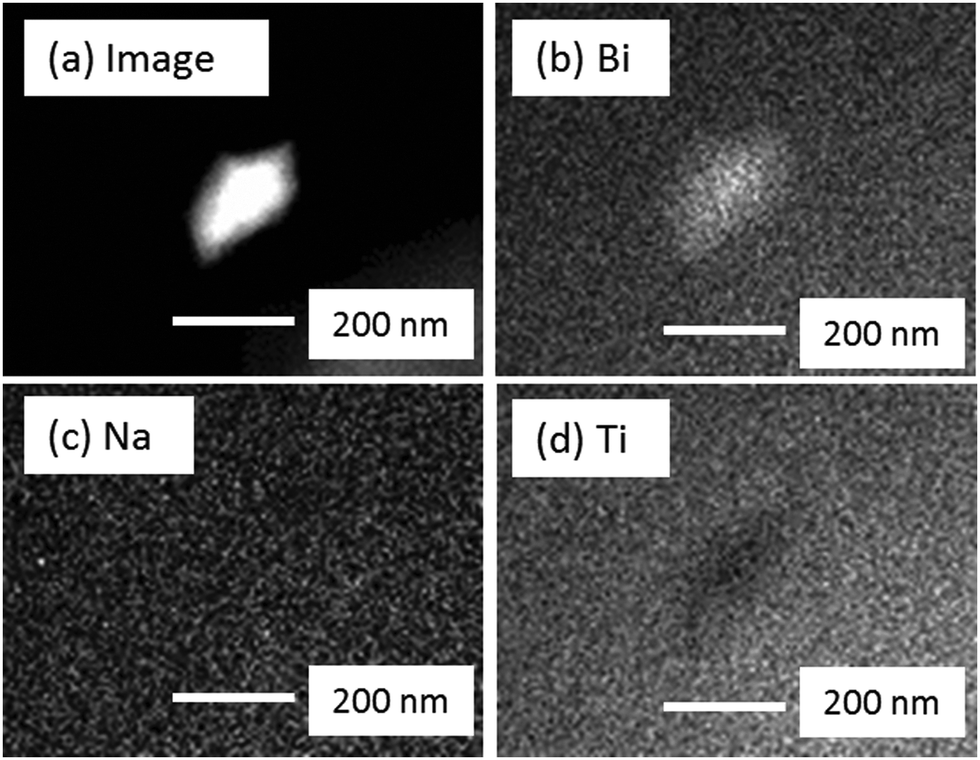 | ||
| Fig. 3 (a) HAADF-STEM (Z-contrast) images for x = 0.01 and EDX mapping results of the same area for (b) Bi-mapping, (c) Na-mapping and (d) Ti-mapping. | ||
XRD and SEM/EDX data were consistent for Na0.50Bi0.50Ti1−yNbyO3+y/2 ceramics for 0.000 ≤ y < 0.030 and showed them to be single-phase. Although XRD data suggested y = 0.030 to be phase-pure, SEM/EDX revealed the presence of an A5B4O15 secondary phase, Fig. 2(e). The average matrix composition for the perovskite phase was Na0.51Bi0.49Ti0.97Nb0.03O3.00 and the A5B4O15 phase contained Nb on the B-sublattice with a slight excess of Na for Bi on the A-sublattice with an average composition of Na0.57Bi4.43Ti3.78Nb0.22O15.04, Table 1. The appearance of a pyrochlore-based ‘Bi2Ti2O7’ phase and A5B4O15 as secondary phases in y ≥ 0.05 was apparent by XRD, Fig. 1(b). SEM/EDX on y = 0.050 revealed the A2B2O7 pyrochlore-type phase to contain Na and Bi on the A-sublattice and Ti and Nb on the B-sublattice with an average composition of Na0.34Bi1.59Ti1.63Nb0.37O6.74 and the average matrix composition for the perovskite phase to be Na0.53Bi0.47Ti0.95Nb0.05O3.00, Table 1 and Fig. 2(f). The average grain size in NBT is ∼5 μm and is substantially reduced with increasing x or y, Fig. 4.
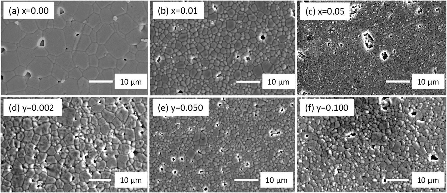 | ||
| Fig. 4 SEM micrographs, (a) to (c) for selected Na0.50Bi0.50+xTiO3+3x/2 and (d) to (f) for selected Na0.50Bi0.50Ti1−yNbyO3+y/2 ceramics. | ||
Complex impedance plane (Z*) plots for the x- and y-series of ceramics at ∼650 °C are shown in Fig. 5. With the exception of x = 0.00, all Z* plots were dominated by a single, large arc with the presence of a small, low frequency (<1 Hz) electrode-type response. The large and dominant arc could be modelled, to a first approximation, on a single parallel resistor–capacitor (RC) element. The associated capacitance value of the arc was consistent with a bulk (grain) response, e.g. Cb ∼ 60–80 pF cm−1 which corresponds to a relative permittivity (εr) value of ∼600 to 800 for paraelectric NBT at this high temperature. The Z* response for x = 0.00 contained bulk, grain boundary and electrode contributions and has been reported previously.27 Here we show only the high frequency Z* response of x = 0.00 at 650 °C, inset to Fig. 5(a), to indicate R of the bulk response (Rb) to be exceptionally low, ∼360 Ω cm as compared to all other ceramics where Rb was a factor of ∼50 to 500 higher, Fig. 5. In the x-series, Rb increases from ∼360 Ω cm for x = 0.00 to ∼100 kΩ cm for x = 0.01 before decreasing to an intermediate value of ∼10–30 kΩ cm for x ≥ 0.02, Fig. 5(a). The variation of Rb with pO2 for x = 0.05 is consistent with n-type electronic behaviour, Fig. 5(b).
 | ||
| Fig. 5 Z* plots of selected (a) Na0.50Bi0.50+xTiO3+3x/2 ceramics, (b) x = 0.05, Type II ceramic, (c) selected Na0.50Bi0.50Ti1−yNbyO3+y/2 ceramics and (d) x = 0.01 and y = 0.050 Type III ceramics. All data were obtained at 650 °C. | ||
For the y-series, Rb increases systematically to ∼15 kΩ cm for y = 0.002, ∼55 kΩ cm for y = 0.003 and a maximum Rb of ∼200 kΩ cm for y = 0.050. It then decreases to ∼160 kΩ cm for y = 0.100 which is similar in magnitude to x = 0.01 and an order of magnitude larger compared to x = 0.05 and y = 0.002 and 0.003, Fig. 5(c).
The low frequency electrode response was most prominent in x = 0.00 (not shown, see ref. 27 for more details) but was also readily observed in x-series, inset Fig. 5(b) and (d), and y ≤ 0.003 ceramics. The presence of a low frequency electrode arc was difficult to resolve for y = 0.050 and 0.100, see inset of Fig. 5(d) for data on y = 0.050.
t ion measurements were performed on all ceramics in the range 600 to 800 °C and are listed in Table 2 together with some previously reported values.27 The behaviour is subdivided into three categories based on the magnitude of tion. Type I, tion ≥ 0.85, predominant oxide-ion conduction, is shown only by x = 0.00; Type II, 0.15 < tion < 0.85, mixed ionic-electronic conduction is shown by x = 0.02, 0.05, y = 0.002 and 0.003; Type III, tion ≤ 0.10, predominant electronic conduction, is shown by x = 0.01, y = 0.020, 0.050 and 0.100.
| Starting composition | t ion (600 °C) | t ion (700 °C) | t ion (800 °C) |
|---|---|---|---|
| Type I, oxygen ion conductor | |||
| x = 0.00 | 0.93 | 0.93 | 0.8527 |
| x = −0.01 | 0.92 | 0.92 | 0.9027 |
| Type II, mixed ionic-electronic conductor | |||
| x = 0.02 | 0.46 | 0.45 | 0.46 |
| x = 0.05 | 0.62 | 0.64 | 0.65 |
| y = 0.002 | 0.57 | 0.63 | 0.63 |
| y = 0.003 | 0.47 | 0.49 | 0.53 |
| Type III, insulator | |||
| x = 0.01 | 0.07 | 0.07 | 0.1027 |
| y = 0.020 | 0.05 | 0.06 | 0.06 |
| y = 0.050 | 0.04 | 0.03 | 0.03 |
| y = 0.100 | 0.02 | 0.02 | 0.03 |
An Arrhenius plot of bulk conductivity values, σb = 1/Rb over a range of temperatures and tion values at 600 °C for both series of ceramics (selected members only for reason of clarity) are shown in Fig. 6. Types I, II and III are clearly distinguished based on a combination of their high, intermediate and low σb and tion values. The variation of εr and tanδ versus temperature for selected ceramics reveal modest changes in εr,max and Tm; however, Type I, II and III behaviour is clearly distinguished based on the magnitude of tanδ above Tm at ∼325 °C, Fig. 7.
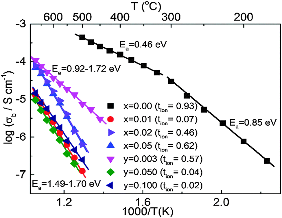 | ||
| Fig. 6 Arrhenius plot of bulk conductivity, σb, versus reciprocal temperature for selected Na0.50Bi0.50+xTiO3+3x/2 and Na0.50Bi0.50Ti1−yNbyO3+y/2 ceramics. Activation energy, Ea, values for σb and tion values at 600 °C are included. | ||
 | ||
| Fig. 7 (a) εr and (b) tanδ (both at 1 MHz) versus temperature for selected Na0.50Bi0.50+xTiO3+3x/2 and Na0.50Bi0.50Ti1−yNbyO3+y/2 ceramics. | ||
Discussion
The XRD and SEM results show the limits of x and y to be low, with x < 0.01 and y < 0.03, Fig. 1 and 2 but they have a dramatic effect on σb, tanδ and tion, Fig. 6, 7 and Table 2, respectively. In the case of simple additions of excess Bi2O3 (x-series), nominally stoichiometric NBT (x = 0.00) transforms from Type I with high σb and tion (600 °C) ∼ 0.93 to Type III with low σb and tion (600 °C) ∼ 0.07 for x = 0.01, Fig. 6. This has very little influence on the εr–T profile but transforms NBT into an excellent high temperature dielectric material with tanδ < 0.02 in the range Tm to ∼650 °C, Fig. 7. Further additions of Bi2O3 excess, e.g. x ≥ 0.02, however exhibit Type II behaviour, with a significant increase in σb and tion (600 °C) > 0.45, Fig. 5(b), 6 and Table 2, and has a deleterious influence on the high temperature dielectric properties with tanδ rising steeply above ∼500 °C and exceeding 10% at 600 °C, Fig. 7.
At this stage it is unclear why starting compositions with x ≥ 0.02 exhibit mixed conduction and higher conductivity but it must be linked to the presence of secondary phases, both of which are Bi-rich compared to NBT, i.e. Na1/2Bi9/2Ti4O15 and a Bi2O3 phase. Two possible explanations are; (i) a change in the Bi-content in the NBT main phase, and (ii) a space-charge model. We outline both below.
Firstly, the Bi-rich secondary phases may deplete the NBT main phase of Bi in x > 0.01, therefore reducing its Bi-content resulting in an increase in oxide-ion conduction. Previous studies have shown that conventional analytical methods such as EDX are unable to distinguish the low level of A-site non-stoichiometry (Na:Bi ratio) required to switch from Type I (x = 0.00) to III (x = 0.01) behaviour in NBT-based ceramics.27 As a consequence, it is not possible to unequivocally prove a change in stoichiometry associated with the main NBT phase in the ceramics, especially due to the fine scale distribution of the Bi2O3-type phase in the x-series, Fig. 2(b) and (d). The level of x required to obtain Type III as opposed to Type I or II behaviour will be dependent on the ceramic processing conditions employed as they control the extent of thermodynamic equilibrium within the ceramics and this will influence the chemical potential and therefore concentration (strictly, the activity) of Bi between the three co-existing phases. In our studies, NBT powders are prepared at ∼850 °C and ceramics are sintered at 1100 to 1150 °C for 2 h in air, covered in sacrificial powder of the same composition. This results in x = 0.00 being Type I and the requirement for a small excess of starting Bi2O3 (x ∼ 0.01) to compensate for losses during processing prior to the formation of Bi-rich secondary phases to obtain Type III behaviour. x values are likely to be significantly different for processing conditions that don't use sacrificial powders to limit Na, Bi volatilisation and/or for higher/longer sintering periods as these factors will influence the final phase assemblage, i.e. composition and weight percentage of the phases present.
Secondly, enhanced ionic conductivity based on a space charge model has been observed in mixtures of two phases, based either on one ionic conductor and one insulator or mixtures of two ionic conductors.32 For example, additions of Al2O3 to lithium iodide LiI led to an increase in ionic conductivity by a factor of ∼50 at room temperature33 and additions of ZrO2 nano-powder to AgI increased ionic conductivity by more than three orders of magnitude at room temperature.34 The interfacial space charge effect is widely considered as a driving force for the enhancement of ionic conductivity.32 This effect may account for the enhanced oxide-ion conduction and the tion of ∼0.4–0.6 in starting compositions with higher Bi-excess (x ≥ 0.02) where NBT, Bi2O3-type and Na0.5Bi4.5Ti4O15-type phases coexist. The fine scale distribution of the Bi2O3-type phase with the NBT matrix, Fig. 2(g) and (h), combined with the fact that many Bi2O3-type materials exhibit high levels of oxide-ion conductivity would appear to be the most likely source of any space charge model in these ceramics. In addition, tion of these ceramics may be overestimated if the Bi2O3-type phase present is a good oxide-ion conductor. Further study is needed to clarify the composition and properties of this Bi2O3-type phase to elucidate its influence on the measured electrical properties of these ceramics and in attempts to try and distinguish between the two possible explanations outlined above.
The trend in behaviour is different for Nb-doping (y-series) compared to excess Bi2O3. Very low levels of Nb-donor doping, e.g. y = 0.002 and 0.003 transform Type I into II, and Type III behaviour is observed for y = 0.010 to 0.100, albeit the Nb-donor doping solid solution limit is y < 0.030, Fig. 1 and 2. Nb-doping is systematic and effective in ‘mopping-up’ and compensating for any oxygen deficiency associated with Bi2O3 loss during processing; tion (600 °C) decreases from 0.93 (undoped) to 0.47 for y = 0.003 and is <0.06 for 0.010 ≤ y ≤ 0.100, Table 2. As a consequence, σb and tanδ remain low for y ≥ 0.010. All ceramics with y ≥ 0.01 retain Type III behaviour and exhibit excellent, high temperature low dielectric loss behaviour above Tm to ∼650 °C, Fig. 7(b). The εr–T profile for y = 0.020 remains similar to undoped NBT, however there is a significant decrease in εr,max for y = 0.050, Fig. 7(a) indicating Nb-doping for Ti influences the lattice polarisability/ferroelectric domain wall motion. Again, the level of y required to suppress oxide-ion conduction in NBT ceramics to promote, high temperature, low dielectric low behaviour will be dependent on the ceramic processing conditions employed.
This study shows that both A-site non-stoichiometry (via excess Bi2O3) and B-site donor-doping (Nb5+ + 1/2O2− → Ti4+) can be effective in fine-tuning the oxide-ion conductivity and tion in NBT. These findings are important for technical applications of NBT-based ceramics. For dielectric applications, some caution is required with the level of excess Bi2O3 in the starting composition as an over excess can lead to a switch from Type III to II behaviour in the presence of Bi-rich secondary phases. Excess Nb-doping therefore offers a more reliable method to retain Type III behaviour to control the level of oxygen vacancies in NBT to ensure low dielectric loss ceramics above Tm to ∼650 °C. The ferroelectric/piezoelectric properties including d33, depolarisation temperature and coercive field can be adjusted by tuning the concentration of oxygen vacancies. Further studies are in progress to establish the ferroelectric and piezoelectric properties of these ceramics. In addition, manufacturing of multilayer actuators with base metal electrodes will require a balanced concentration of oxygen vacancy to increase resistance to reduction for titanium under lower pO2 to avoid n-type semiconductivity as well as to minimise performance degradation associated with oxygen vacancies.
It is worth noting that NBT-based ceramics can be mixed conducting, albeit with a low electronic carrier concentration, e.g. x = 0.02, 0.05, y = 0.002 and 0.003, Fig. 6 and Table 2. Although σb is low, the associated activation energy, Ea, for bulk conduction is high, e.g. >0.9 eV and tanδ remains low below ∼500 °C, see Type II in Fig. 7(b), there remains a level of mobile oxygen vacancies that contribute appreciably to σb, as readily detected by EMF measurements, Table 2. An indication of the presence of ionic conduction in the x-series ceramics (where tion can be as low as 0.07 for Type III) can be obtained from low frequency (<1 Hz) IS measurements at elevated temperatures, as shown in the Z* plots in the insets of Fig. 5(b) and (d) for Types II and III, respectively. In the case of y-series ceramics with Type III behaviour with tion < 0.05, the presence of ionic conduction was not readily observed by low frequency IS data, see inset of Z* plot for y = 0.050 in Fig. 5(d). This highlights the value of performing EMF measurements in A-site non-stoichiometric perovskites that contain volatile species, such as Na, K, Bi and Pb, where modest levels of oxide-ion conduction (e.g. ∼5% of σb) may be present.
Conclusions
We recently showed that the oxygen vacancies in the nominal starting NBT composition associated with Bi2O3-loss generated during sample processing can be suppressed by a small Bi-excess in the nominal starting composition (Na0.50Bi0.50+xTiO3+3x/2, x = 0.01) or by Nb-donor doping (Na0.50Bi0.50Ti1−yNbyO3+y/2, 0.005 ≤ y ≤ 0.030). In this work we show that further increasing the starting Bi-content (0.02 ≤ x ≤ 0.10) induces mixed ionic/electronic behaviour by reintroducing higher oxide-ion conductivity with tion ∼ 0.4–0.6. For Nb-doping, mixed conduction is observed at low doping levels (y ≤ 0.003). In contrast to increasing the Bi-excess content, increasing the Nb-donor doping level to y = 0.050, 0.100 systematically suppresses oxide-ion conductivity with tion ≤ 0.05. The results show NBT compositions can be tuned smoothly to exhibit tion from near unity to zero. This study provides guidelines on fine-control of oxygen vacancies in NBT-based materials to tune electrical, dielectric and piezoelectric properties and to improve manufacturing practices.Acknowledgements
The authors thank the EPSRC (EP/L017563/1) for funding.References
- P. Kofstad, Nonstoichiometry, diffusion, and electrical conductivity in binary metal oxides, Wiley-Interscience, New York, 1972 Search PubMed.
- D. M. Smyth, The defect chemistry of metal oxides, Oxford University Press, 2000 Search PubMed.
- A. J. Moulson and J. M. Herbert, Electroceramics: materials, properties, applications, John Wiley & Sons, 2003 Search PubMed.
- H. Kishi, Y. Mizuno and H. Chazono, Jpn. J. Appl. Phys., 2003, 42, 1–15 CrossRef CAS.
- M. Li, H. Zhang, S. N. Cook, L. Li, J. A. Kilner, I. M. Reaney and D. C. Sinclair, Chem. Mater., 2015, 27, 629–634 CrossRef CAS.
- T. Kimura, E. Fukuchi and T. Tani, Jpn. J. Appl. Phys., 2005, 44, 8055–8061 CrossRef CAS.
- F. Kulcsar, J. Am. Ceram. Soc., 1959, 42, 343–349 CrossRef CAS.
- G. H. Haertling and C. E. Land, J. Am. Ceram. Soc., 1971, 54, 1–11 CrossRef CAS.
- M. Li, L. Li, J. Zang and D. C. Sinclair, Appl. Phys. Lett., 2015, 106, 102904 CrossRef.
- B. Jaffe, W. R. Cook and H. Jaffe, Piezoelectric ceramics, Academic Press, 1971 Search PubMed.
- T. Rojac, S. Drnovsek, A. Bencan, B. Malic and D. Damjanovic, Phys. Rev. B: Condens. Matter Mater. Phys., 2016, 93, 014102 CrossRef.
- G. O. Jones and P. A. Thomas, Acta Crystallogr., Sect. B: Struct. Sci., 2002, 58, 168–178 CAS.
- J. A. Zvirgzds, P. P. Kapostin, J. V. Zvirgzde and T. V. Kruzina, Ferroelectrics, 1982, 40, 75–77 CrossRef CAS.
- E. Aksel, J. S. Forrester, B. Kowalski, J. L. Jones and P. A. Thomas, Appl. Phys. Lett., 2011, 99, 222901 CrossRef.
- I. P. Pronin, P. P. Syrnikov, V. A. Isupov, V. M. Egorov and N. V. Zaitseva, Ferroelectrics, 1980, 25, 395–397 CrossRef CAS.
- S. B. Vakhrushev, V. A. Isupov, B. E. Kvyatkovsky, N. M. Okuneva, I. P. Pronin, G. A. Smolensky and P. P. Syrnikov, Ferroelectrics, 1985, 63, 153–160 CrossRef CAS.
- J. Suchanicz, K. Roleder, A. Kania and J. Hańaderek, Ferroelectrics, 1988, 77, 107–110 CrossRef CAS.
- J. Suchanicz and W. S. Ptak, Ferroelectr., Lett. Sect., 1990, 12, 71–78 CrossRef CAS.
- G. O. Jones, J. Kreisel, V. Jennings, M. A. Geday, P. A. Thomas and A. M. Glazer, Ferroelectrics, 2002, 270, 191–196 CrossRef CAS.
- J. Suchanicz and J. Kwapulinski, Ferroelectrics, 1995, 165, 249–253 CrossRef CAS.
- J. Suchanicz, Ferroelectrics, 1995, 172, 455–458 CrossRef CAS.
- E. Aksel, J. S. Forrester, J. C. Nino, K. Page, D. P. Shoemaker and J. L. Jones, Phys. Rev. B: Condens. Matter Mater. Phys., 2013, 87, 104113 CrossRef.
- I. Levin and I. M. Reaney, Adv. Funct. Mater., 2012, 22, 3445–3452 CrossRef CAS.
- S. Gorfman and P. A. Thomas, J. Appl. Crystallogr., 2010, 43, 1409–1414 CrossRef CAS.
- E. Aksel, J. S. Forrester, J. L. Jones, P. A. Thomas, K. Page and M. R. Suchomel, Appl. Phys. Lett., 2011, 98, 13–16 CrossRef.
- B. N. Rao, R. Datta, S. S. Chandrashekaran, D. K. Mishra, V. Sathe, A. Senyshyn and R. Ranjan, Phys. Rev. B: Condens. Matter Mater. Phys., 2013, 88, 224103 CrossRef.
- M. Li, M. J. Pietrowski, R. A. De Souza, H. Zhang, I. M. Reaney, S. N. Cook, J. A. Kilner and D. C. Sinclair, Nat. Mater., 2014, 13, 31–35 CrossRef CAS PubMed.
- Y. Hiruma, H. Nagata and T. Takenaka, J. Appl. Phys., 2009, 105, 084112 CrossRef.
- J. Petzelt, S. Kamba, J. Fabry, D. Noujni, V. Porokhonskyy, A. Pashkin, I. Franke, K. Roleder, J. Suchanicz, R. Klein, G. E. Kugel and J. Fábry, J. Phys.: Condens. Matter, 2004, 16, 2719–2731 CrossRef CAS.
- J. Zang, M. Li, D. C. Sinclair, T. Frömling, W. Jo and J. Rödel, J. Am. Ceram. Soc., 2014, 97, 2825–2831 CrossRef CAS.
- V. A. Isupov, Ferroelectrics, 2005, 315, 123–147 CrossRef CAS.
- J. Maier, Prog. Solid State Chem., 1995, 23, 171–263 CrossRef CAS.
- C. C. Liang, J. Electrochem. Soc., 1973, 120, 1289–1292 CrossRef CAS.
- K. Tadagana, K. Imai, M. Tatsumisago and T. Minami, J. Electrochem. Soc., 2000, 147, 4061–4064 CrossRef.
| This journal is © The Royal Society of Chemistry 2016 |