
 Open Access Article
 This Open Access Article is licensed under a Creative Commons Attribution-Non Commercial 3.0 Unported Licence
Progress in pulsed laser deposited two-dimensional layered materials for device applications
Zhibin
Yang
ab and
Jianhua
Hao
*ab
aDepartment of Applied Physics, The Hong Kong Polytechnic University, Hung Hom, Hong Kong, P. R. China. E-mail: jh.hao@polyu.edu.hk
bThe Hong Kong Polytechnic University, Shenzhen Research Institute, Shenzhen 518057, P. R. China
First published on 31st August 2016
Abstract
During the past decades, atomically thin, two-dimensional (2D) layered materials have been intriguing researchers for both fundamental study and practical applications, because of their extraordinary mechanical, thermal, electrical and optical properties, which are distinct from their counterparts in bulk materials. To realize the device demonstration based on 2D materials, some methods to produce 2D layers have been developed, such as mechanical exfoliation, solution based exfoliation, chemical vapour deposition (CVD) and so on. Among these methods, the physical bottom-up synthesis technique, namely pulsed laser deposition (PLD), routinely used for growing complex oxide thin films has been proved to be an alternative way to the most reported CVD method for obtaining ultrathin 2D layered films, because of its remarkable advantages. In this review, recent advances of preparing 2D materials by PLD are presented, including deposition processes, structure and characterization. We introduce the performance of proof-of-concept electronic or optoelectronic devices based on various kinds of 2D layers and ultrathin films grown using PLD and these include graphene, transition metal dichalcogenides, hexagonal boron nitride, gallium selenide, and black phosphorus. Some challenging issues are discussed and directions for future investigation are suggested.
1. Introduction
In the past few decades, the development of information technology has been following the observation known as Moore's law, which states that the number of transistors on a single computer chip will double every two years.1–3 However, the prediction is getting closer to the end in recent years, because overheating of the electronic devices is unavoidable when more and more silicon (Si)-based circuits are integrated together into a tiny area, and the small sized transistors largely increase the manufacturing cost.4–6 In order to solve these problems, a number of new materials have been explored to provide an alternative to Si, which could be fabricated into devices as fast as traditional Si-based electronics and also generate less heat.Two-dimensional (2D) material is one of most attractive materials which has been used for both fundamental study and practical applications over the past decade, and is regarded as a promising candidate for the next generation of electronics and optoelectronics at the 2D limit.7–10 2D material is defined as atomically thin, layered crystalline sheets, with van der Waals (vdW) interactions between the layers. Graphene was the first 2D material to be discovered, which is composed of a single layer of sp2 hybridized carbon atoms, showing excellent mechanical, thermal, electrical properties and high chemical stability and is still the leader out of all of the atomic sheets.7,8,11–13 However, the main drawback of using graphene is the lack of an intrinsic energy band gap, which is crucial for the electronic materials used for transistor development. Thus, a fundamental problem of a graphene-based transistor is that the device remains conducting even when it is switched off. Consequently, a low on/off current ratio makes its use in digital logic devices unrealistic. This issue has motivated many researchers around world to search for other layered materials beyond graphene, which possess an energy band gap with a semiconducting nature. To date, several groups of 2D materials, including transition metal dichalcogenides (MX2; TMDs),14–16 phosphorene,17–19 and silicone,20,21 have shown a sizeable band gap value and good electronic properties, whereas hexagonal boron nitride (h-BN)22,23 has promising dielectric properties for use as a gate insulator (Fig. 1a). These materials can be categorized as being 2D because they represent the thinnest isolated crystalline form, without surface dangling bonds, and have outstanding transport properties within the intralayer.9,24 The portfolio of the novel 2D materials and their hybrid structure is still growing, arousing a technology evolution of almost everything related to energy, electronics and photonics.6,25 Compared to the Si routinely employed in modern electronics, 2D materials have the advantages of occupying a small space and have a smaller energy consumption. Furthermore, when the thickness of these materials is reduced to few layers, spintronics, namely the transfer process involved by electron spins rather than the flow of charge carriers, could be considered for designing some novel transistors.26–28
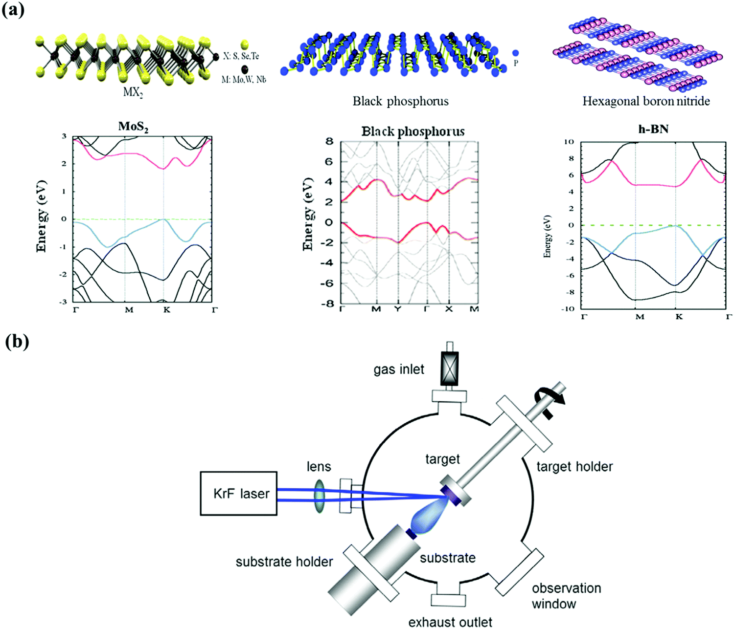 | ||
| Fig. 1 (a) Schematic of atomic structures of 2D materials [dichalcogenides (MX2), black phosphorus (BP), hexagonal boron nitride (h-BN)], and the electronic band structure of monolayer molybdenum disulfide (MoS2), BP and h-BN. Reproduced from ref. 22, 24 and 52 with permission from the Royal Society of Chemistry. (b) Schematic of a PLD system. Reproduced with the permission of the publishers of ref. 80. | ||
Up to now, most of the work reported on 2D materials has been conducted on the basis of research laboratory fabrication and testing. To satisfy the requirement of device applications, numerous studies have focused extensively on exploring the fabrication methods capable of providing large scale, high yield and low cost ultrathin 2D nanosheets. One of the commonly used techniques in the synthesis of nanostructures is vapor deposition, which refers to the synthesis process exploiting vapor phase source materials to form solid films using condensation or chemical reactions.29 Previous reviews on the bottom-up synthesis of 2D materials mainly refer to chemical vapor deposition (CVD).30–32 Up to now, there has been no review providing a comprehensive coverage of physical vapor deposition (PVD) methods for making 2D materials. Therefore, in this review, a systematic overview of the recent efforts, progress, opportunities and challenges in the fabrication of 2D layered materials using pulsed laser deposition (PLD) as one of the typical PVD methods will be presented. Initially, the operation principles and scope of application of PLD will be described. After that, from Section 3 to Section 7, the advances in preparing atomically thin nanosheets using PLD will be highlighted including the synthesis process, structure and device characterization, which will be illustrated based on the different types of 2D materials. Lastly, some strategies in improving the performance of PLD grown, 2D layered films and potential research directions in the future will be discussed.
2. Overview of PLD for 2D films
Since the successful synthesis of high temperature superconducting yttrium barium copper oxide (YBa2Cu3O7) films in an efficient and epitaxial way,33 PLD has become one of the most widely used techniques for the deposition of complex oxide thin films,34–37 heterostructures,38–43 and well controlled interfaces.44 As shown in Fig. 1b, the PLD system mainly consists of an ultrahigh vacuum chamber and a high energy pulsed laser. In principle, the mechanism of PLD includes a series of complex physical reactions. Briefly, when the focused laser beam strikes the surface of a solid target for a short time, an energetic plasma plume is formed with ions and atoms, and then collected on a pre-heated substrate placed in front of the target. Depending on the substrate temperature and other factors, a single-crystal, polycrystalline, or amorphous film can be obtained.45 The quality of the films deposited by PLD is strongly influenced by a number of experimental parameters. For example, the parameters of the pulsed laser source (wavelength, fluence, frequency, pulse duration, and so on) have notable effects on the laser/target interaction.46–48 In the case of an ultrashort pulse duration, such as the femtosecond (fs) laser, there is little interaction between the plume and incoming laser because the time for the plasma to be generated is longer than the pulse duration.48 Despite the attractive features of PLD, the large droplets induced by the laser ablation have a significant negative impact on the surface morphology of the film. To minimize this effect, numerous methods have been developed, such as using off-axis geometry,49 inserting a shadow mask,50 or using a dense and smooth target.51Besides using PLD for the deposition of complex oxide thin films, it should be noted that PLD has been considered for use in the synthesis of layered 2D materials over recent years. Up to now, the main techniques used for realizing mono- or few layered nanosheets include mechanical exfoliation,52–54 chemical exfoliation,55,56 liquid-based exfoliation,57–59 CVD,30–32,60,61 and PVD.62–64 For wafer scale fabrication of 2D materials, CVD and PVD are commonly used in bottom-up techniques. The main disadvantage of CVD is its process in harsh growth environment, such as high reaction temperature and long growth time, which lead to considerable experimental difficulty. Comparing with CVD, PVD utilizes pure physical method to prepare large scale thin films mainly under higher vacuum and lower growth temperature. Up to now, 2D materials, including graphene,62 molybdenum disulfide (MoS2),63 molybdenum sulfoselenide (MoS2Se2)64 and so on, have been successfully realized by using various PVD techniques. Compared with these methods, PLD exhibits its own features and scope of application. Table 1 shows the comparison of growth conditions and material quality for 2D materials made using different fabrication techniques. Compared to CVD, the advantages of using PLD include high growth rate, low cost, good control of thickness and morphology, and low growth temperature, and it is applicable to versatile materials, especially for those with chemical active surface. In addition, it is easier to make composites using PLD, because different targets can be installed inside the chamber simultaneously. In comparison to other PVD methods (thermal evaporation, sputtering, and so on), PLD exhibits specific characteristics in two important aspects. Firstly, the synthesis is a pulsed mode, meaning that a small amount material could be grown in a few microseconds. Secondly, because of the fast and strong heating of the target, stoichiometric growth could be readily achieved by using PLD.
| Size | Throughput | Thickness homogeneity | Fabrication rate | Processing temperature | Ref. | |
|---|---|---|---|---|---|---|
| Mechanical exfoliation | 1–10 μm | Low | Low | Fast | RT | 52–54 |
| Chemical exfoliation | 1–10 μm | High | Moderate | Moderate | RT | 55 and 56 |
| Liquid exfoliation | 1–10 μm | High | Moderate | Moderate | RT | 57–59 |
| CVD | Over 10 cm | High | Very high | Low | High | 30–32, 60 and 61 |
| PVD | Over 10 cm | High | High | Moderate | Moderate | 62–64 |
| PLD | Up to 1 cm | High | High | Fast | Moderate | 33–45 |
Further to the previous brief background information on PLD, next the preparation of atomically thin layered films using PLD and their corresponding applications as a sequence of the 2D types, including graphene, TMDs, h-BN, gallium(II) selenide (GaSe), and black phosphorus (BP), will be introduced.
3. Graphene grown using PLD
Graphene has been made using PLD since 2005, and this is earlier than the first attempt at growth using CVD in 2009.65 Cappelli et al. studied the influence of substrate temperature on the resultant carbon films grown using PLD from a pyrolytic graphite target.65 The Raman spectroscopy and near-edge X-ray absorption fine structure results revealed that graphene sheets could be obtained at 900 °C, which exhibited a trend to grow along the direction of the perpendicular to the top surface of a Si substrate. Following this work, Scilletta et al. reported that the formation and texture of the graphene nanosheets could be affected by the fabrication temperature and atmosphere gas.66 According to X-ray diffraction (XRD) results, graphene nanosheets appeared at a high temperature in vacuum. Whereas for thin films made in a helium gas atmosphere, only graphene particles were characterized, which were embedded in the amorphous carbon film. However, the thickness of the nano-graphene obtained at this stage is about a few hundreds of a nanometer thick,67 which exceeds the scope of 2D materials.3.1 Graphene grown on a metal substrate
Since the high quality monolayer graphene was synthesized on an iridium(111) substrate using the CVD method,68 transition metals have become quite commonly used substrates for fabricating graphene because of their high uniformity and ease of transferring to other substrates for subsequent device fabrication. Polycrystalline cobalt and nickel (Ni) thin films are generally used because of their high carbon solubility, low cost and ease of fabrication into electronic devices. As the CVD methods require a long growth time and high temperature, researchers started to consider growing graphene on metal substrates using PLD as an alternative to CVD.69–74 At an early stage, Koh et al. grew graphene with a few layers (<5 layers) on Ni (600 nm)/Si substrate using PLD.69 They studied the influence of cooling rate and laser energy on the formation and quality of the graphene layers. The schematic in Fig. 2a shows that the mechanism of graphene layer formation on a metal substrate can be illustrated by the interactions between the carbon atoms and the metal layer.71 As the laser pulses struck the graphite target, the plasma plume was ejected which contained carbon ions which were bombarding the substrate surface and then penetrated deeply into the layer of Ni. With a higher cooling rate, the carbon species were separated from Ni film because of the decreasing solubility of carbon in Ni. The precipitated carbon atoms on the Ni surface were organized to assemble into graphene layers, and the Raman spectra shown in Fig. 2b show this. Whereas for the synthesis process with a lower cooling rate, less carbon species were precipitated on to the surface of the Ni film, resulting in more defects in the grown graphene film. According to the study, cooling rate is one of the key factors in determining the quality of graphene with few layers grown on the metal substrates using PLD.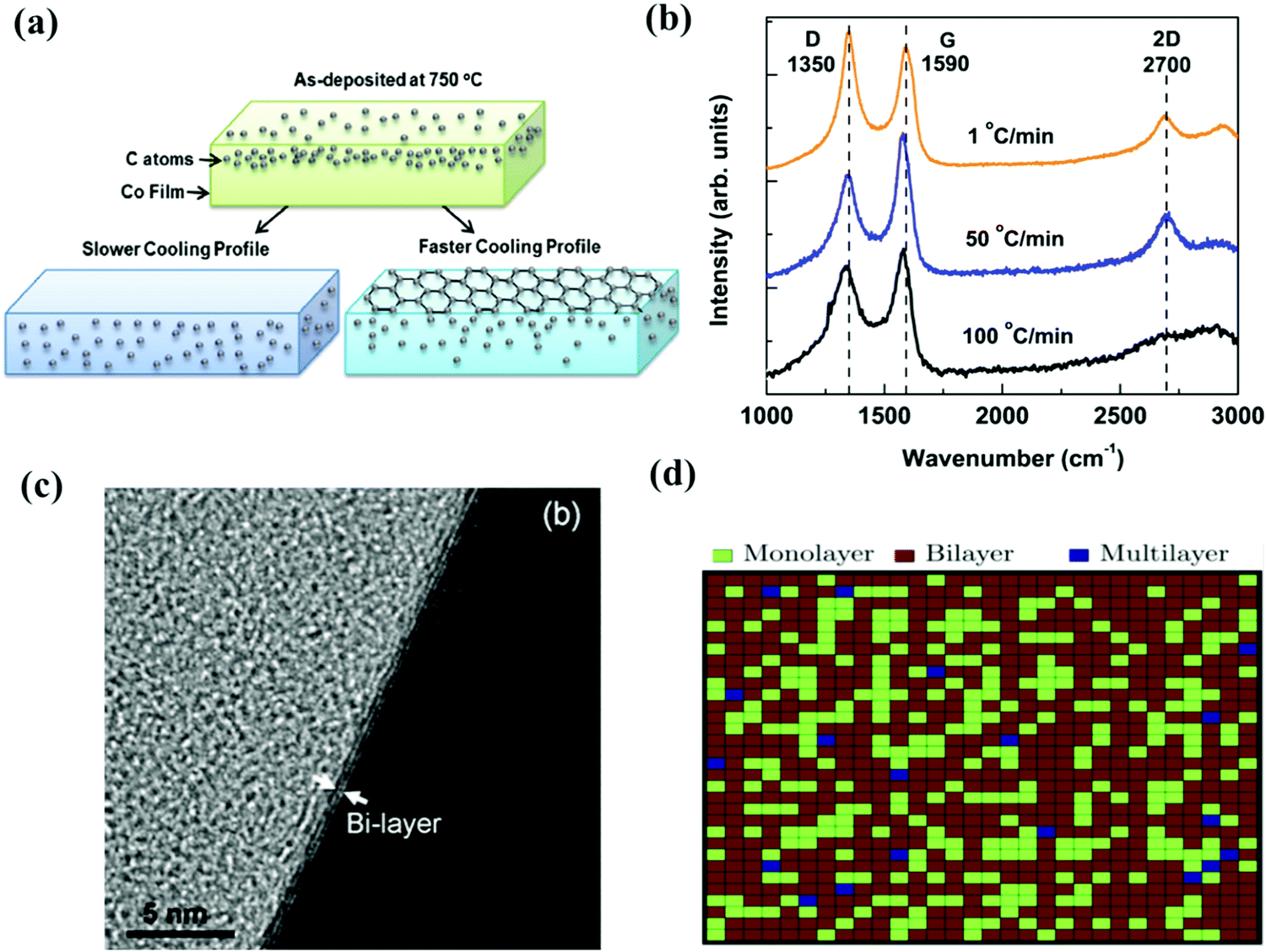 | ||
| Fig. 2 (a) Illustration of the mechanism of formation of graphene. Reproduced from ref. 71 with permission from Elsevier. (b) Raman spectra of graphene deposited with different cooling rates. Reproduced with permission of the publishers of ref. 69. (c) Cross-sectional HRTEM image of bi-layer graphene produced using PLD. Reproduced with permission of the publishers of ref. 70. (d) 2D mapping of intensity ratio of G to 2D Raman peaks. Reproduced with permission of the publishers of ref. 72. | ||
In a further study, Wang et al. reported that graphene with few layers was grown on a Ni substrate under a lower temperature, and the thickness of the film could be easily controlled by adjusting the proportion of the thickness of Ni to the carbon layers.70 Ultrathin graphene films (less than five layers) were synthesized by decreasing the carbon proportion or increasing the initial thickness of the Ni film and the results are shown in high-resolution transmission electron microscopy (HRTEM) images (Fig. 2c). Apart from Ni substrates, graphene was also realized on some other metal substrates.71
Usually, in order to apply metal substrate based graphene to devices, a transfer process is required, which may induce defects to the graphene film during the process and thus influence its electronic properties. It is notable that Hemani et al. have developed a new method to grow graphene directly on silicon dioxide (SiO2) substrates.72 As a catalytic layer, a Ni film (300 nm) was sputtered on to SiO2 (300 nm)/Si substrate for further graphene deposition. As illustrated by scanning electron microscopy (SEM) and Raman spectroscopy, graphene was grown on both the Ni film surface and the Ni/SiO2 interface. By etching the Ni film off, the interfacial bilayer graphene was deposited directly on to the SiO2/Si substrate. High quality graphene synthesized by this process has been verified using Raman mapping (Fig. 2d) and X-ray photoelectron spectroscopy (XPS) results. A similar method was applied to grow multi-layer, textured graphene films on n-doped Si substrate.75 For the first step, an amorphous carbon film was deposited on a Ni layer buffered Si substrate using PLD. Subsequently, the graphene was converted from the carbon film using a post-annealing process. The graphene obtained could be directly used as electrodes for electrochemical applications without needing a transfer process.
3.2 Graphene grown directly on insulating substrates
Although etching the catalytic layer can leave out the transfer process for metal substrate based graphene, the etchant may also degrade the graphene layers and eventually be detrimental to the performance of the device. Therefore, the process for direct growth of graphene film on those substrates possessing practical importance is desirable for integrating graphene into electronic devices.76–82 Recently, by using a laser ablation method, graphene was directly grown on a Si substrate by Qian et al., with the help of a flowing argon (Ar) gas as background.76 As shown in Fig. 3a, the Raman spectrum shows the featured peaks of few layers of graphene, and the cross-sectional transmission electron microscopy (TEM) image (Fig. 3b) confirms that the film obtained corresponds to around 10 layers of graphene. The formation of graphene on Si-based substrates strongly depends on the laser fluence. On the whole, with a laser fluence below 1.0 J cm−2, only small carbon clusters were struck off from the highly ordered pyrolytic graphite (HOPG) target, resulting in the formation of amorphous carbon. When the laser energy as increased, graphene films were deposited using a large sheet species with a layered structure, exfoliated from the target. Because the photon energy of the laser used (532 nm) was smaller than the C–C bond energy, the laser pulses were unable to break the chemical bond of the HOPG. Therefore, the interaction between the pulsed laser and the target material can be explained by the photo-thermal process.76 An alternative research effort has been devoted to making graphene film by using an ultraviolet (UV) pulsed laser without any catalytic materials.78 A krypton fluoride (KrF) laser with a wavelength of 248 nm was employed to grow graphene on various Si-based substrates. Raman spectra (Fig. 3c) and SEM images indicate the production of graphene films with high uniformity. The mechanism of graphene formation can be explained by the bond breaking of the HOPG target induced by the photoelectronic excitation.78 When the high energy laser pulses hit the target surface, a large amount of carbon ions and clusters might be generated and projected towards the substrate. The carbon species with a low kinetic energy would nucleate a few layers of graphene on the substrate. Furthermore, the high temperature of the substrate can assist in reducing the defects of the film, and thus the formation of a layered structure could be encouraged. As shown in Fig. 3d, the electrical resistivity increases with the enhanced laser fluence, which is an evidence of low defect density. Following on from the previous study, Kumar and Khare have reduced the graphene obtained to five layers by adjusting the growth temperature.79 The scale and thickness of graphene can be accurately modulated by the laser fluences, substrate temperature and ablation time.79–82 As well as fabrication with laser ablation and re-condensation strategy, laser reduction is another method used to produce 2D layers. Kymakis et al. have prepared a few layer flexible and transparent graphene oxide (GO) electrodes by using a femtosecond laser to irradiate the spin coated GO film on a poly(ethylene terephthalate) substrate.83 By considering the ultra short pulse duration of femtosecond laser, much less electron–phonon coupling is occurring during the laser pulse compared with the nanosecond laser, which results predominantly in non-thermal excitation effects. The laser reduced GO film shows high conductivity and transmittance, making it compatible to be utilized with a flexible device. Using results from recent studies performed by several research groups, the growth conditions, morphology and properties of PLD grown graphene on both metal and insulating substrates are summarized in Table 2.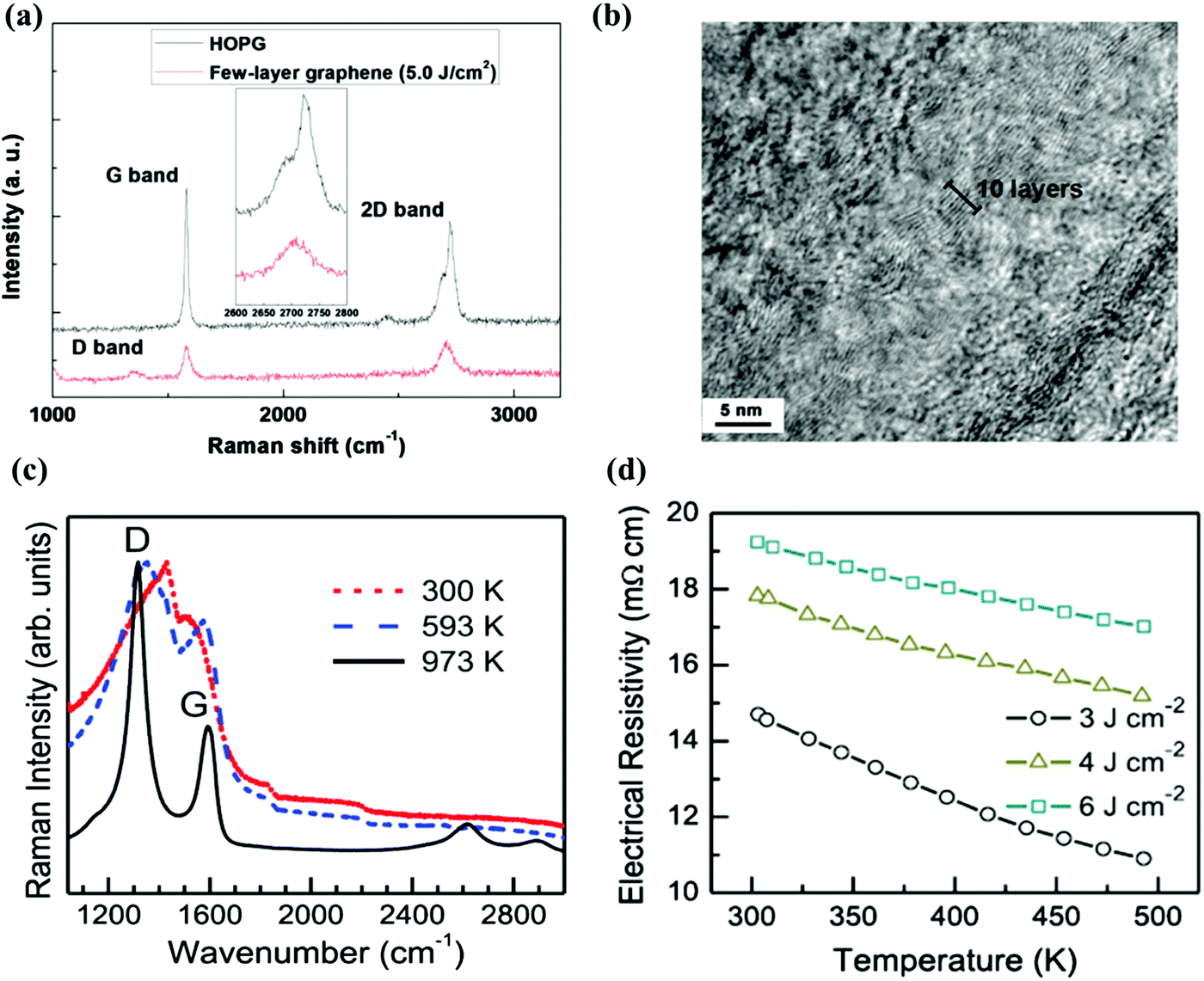 | ||
| Fig. 3 (a) Comparison of Raman spectra of a graphene with few layers grown on an Si substrate and a HOPG crystal. The inset image shows the enlarged 2D band region. (b) HRTEM images of graphene produced using PLD. Reproduced with permission of the publishers of ref. 76. (c) Raman spectra of PLD grown films under different processing temperatures. (d) Relationship between electrical resistivity and temperature of graphene films grown using three different laser fluences. Reproduced with permission of the publishers of ref. 78. | ||
| Growth temperature (°C) | Base pressure (Pa) | Laser energy | Background gases | Morphology | Optical/electrical properties | Ref. | |
|---|---|---|---|---|---|---|---|
| Graphene/Si〈100〉 | 900 | ∼10−5 | 7 J cm−2 | None | Nano sized graphene clusters | — | 65 |
| Graphene/Ni (600 nm)/n-Si | 750 | 6.65 × 10⁻⁴ | 50 mJ | None | <five layers of graphene | — | 69 |
| Graphene/Cu | 400 | 1.33 × 10⁻⁴ | — | None | Sharp folded graphene nano-structure | Turn on voltage of field emission: Eon = 1.4 V μm−1 | 71 |
| Graphene/SiO2/Si | 700 | 1.33 × 10⁻⁶ | 6 J cm−2 | 20 mTorr Ar (5 N) | Three to four layers of graphene with a smooth surface | Electrical conductivity at 300 K = 52.63 S cm−1 | 76 |
| Graphene/SiNx/Si | 700 | — | 6.1 J cm−2 | 20 mTorr Ar or 20, 100, 250, and 500 mTorr N2 | In plane nano-structured graphene with defects | Electrical conductivity at 300 K = 70.02 S cm−1 | 84 |
| Graphene/sapphire | 600 | 1.33 × 10⁻³ | 1.2 J cm−2 | None | Three graphene layers obtained | — | 82 |
3.3 Applications of graphene grown by PLD
It is well known that the p–n junction is a basic component in many electronic and optoelectronic device applications. Recently, Kumar et al. fabricated graphene films into p–n junctions for device characterization.84 The graphene film was deposited on SiNx/Si substrates with the background gases of Ar or nitrogen (N2). For the graphene grown in Ar, the positive Seebeck coefficient measurement indicates p-type conduction (Fig. 4a). However, the graphene grown under an N2 environment exhibits an n-type semiconducting behavior, which might arise from the nitrogen doping during the deposition of the film. According to the XRD and XPS results, graphene is doped by substituting carbon with nitrogen atoms. The nitrogen incorporated can also help to reduce the defects of graphene revealed by the Raman spectra. As nitrogen doping can provide extra electrons, n-type graphene shows a higher conductivity compared to the non-doped graphene film grown in Ar gas. The p–n junction diodes based on the graphene films obtained showed a diode-like, non-linear rectifying behavior (Fig. 4b), which was induced by the increased difference in Seebeck coefficient of p- and n-type films.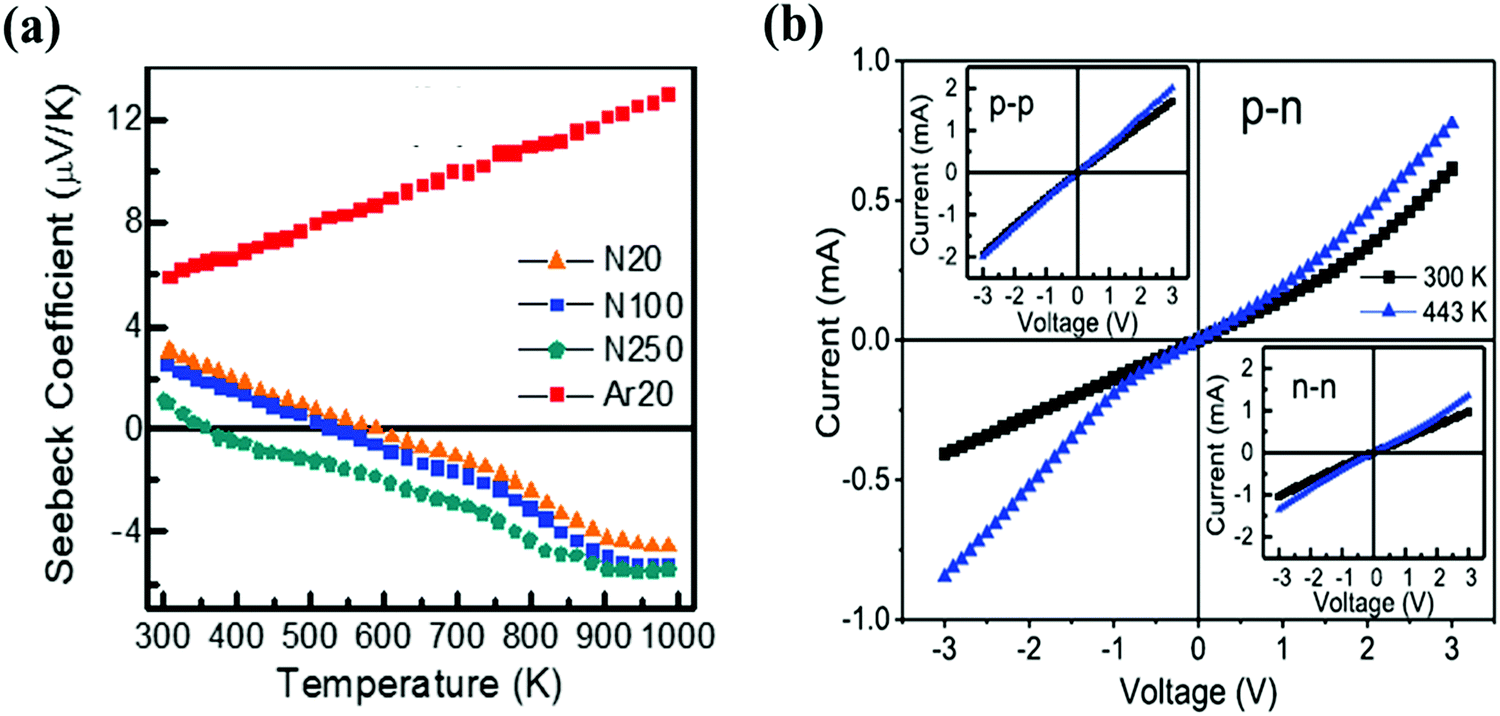 | ||
| Fig. 4 (a) Temperature dependence of the Seebeck coefficient of graphene thin films grown under different background gases. (b) Current versus voltage characteristic of the p–n junction produced using PLD grown graphene. The bottom-right and top-left inset figures show the output characteristics of the n-type and p-type PLD grown graphene, respectively. Reproduced with permission of the publishers of ref. 84. | ||
The good conductivity of graphene grown using PLD makes it promising for field emission (FE) and sensor applications.73,85 Few layer graphene with a sharp folded nanostructure was deposited on copper (Cu) substrates.73 After being transferred to a SiO2/Si substrate, the sharp folded graphene nanoribbon shows good FE performance with a turn-on field of 1.4 V μm−1, because of the presence of a large number of emission sites in the sharp edges. For sensing applications, a photo-detection device based on a graphene–silicon Schottky diode was developed using laser ablation. As a result, the photo sensitivity of the PLD grown graphene/p-Si diode reached up to 380%, which is superior to that of a junction based on mechanical exfoliated graphene.85 Furthermore, with periodic illustration of laser beam, remarkable on/off photocurrent switching and good response time were observed, indicating the potential of fast and effective photo-sensing from the graphene/p-Si diode.
Because of its high adsorption capacity, graphene has been widely used in applications for environmental clean-up as well.86 Recently, Tite et al. have applied the PLD grown graphene to detect the deltamethrin concentration in cultured human keratinocyte cells.87 Graphene with few layers was obtained by post-annealing amorphous carbon film, which was directly deposited on an Si substrate using PLD. Gold nanoparticles were decorated on the graphene surface to improve the sensitivity. As a result, the Raman spectra feature peaks of graphene with an observably enhanced intensity in the presence of increasing deltamethrin concentrations, indicating that the insecticide can be detected at the concentration below the cytotoxic dose.
4. 2D TMDs grown using PLD
The 2D TMDs have attracted a lot of interest because of their outstanding mechanical, thermal, optical and electrical properties, which are distinct from their corresponding bulk materials.14–16 In recent years, MoS2 and tungsten disulfide (WS2) have been most extensively studied for both their fundamental properties and potential applications because of their considerable band gap and high carrier mobility. For the time being, the synthesis of large area uniform MoS2 and WS2 thin films are mainly achieved using a CVD technique. In the following part of this section, the fabrication process and applications of MoS2 and WS2 thin films produced using PLD as an alternative route to CVD will be reviewed.4.1 Layered MoS2 thin films grown using PLD
The early stages of synthesis of MoS2 thin films employing pulsed laser can be dated back to the twentieth century.88–91 As far back as 1988, MoS2 thin films were deposited on stainless steel substrates using PLD under a fairly low growth temperature (300 °C).88 The films showed the same stoichiometry as the MoS2 target. However, the internal structure of the film was unknown and the thickness was too large compared to the scope of 2D materials.Since MoS2 was re-evaluated and realized as a new member of layered 2D materials, the ultrathin films of MoS2 were obtained using PLD and the number of deposited layers can be controlled.92–101 Loh and Chua attempted to grow MoS2 on various metal substrates, [aluminium, silver (Ag), Ni, Cu, and so on] which were chosen because of their smaller lattice mismatch.92 A KrF excimer laser with energy of 50 mJ was used to irradiate a MoS2 target (99.9% purity). According to the Raman spectroscopy results (Fig. 5a), highly crystalline 2H-MoS2 layers were obtained on Ag substrates only, and the film grown can be as thin as two to three layers, which was confirmed by the cross-sectional TEM image (Fig. 5b). In contrast to graphene, the mechanism of MoS2 deposited using PLD is complicated because two types of element atoms or clusters are generated and the sulfur species form other compounds easier by reacting with the metal substrate. When sulfur atoms arrive the surface of the Ag substrate, a layer of silver sulfide (Ag2S) is formed, which was verified by XPS results (Fig. 5c), which become an excellent template for the growth of MoS2 thin films, which is surprising when considering the infinitesimal lattice mismatch between them. With high uniformity and large grain size, the quality of few layer MoS2 supported by an Ag substrate grown using PLD is comparable to the films grown using CVD. Whereas for other metal substrates, a native oxide layer covering the metal surface will form an energy barrier to obstruct the crystallization of MoS2.
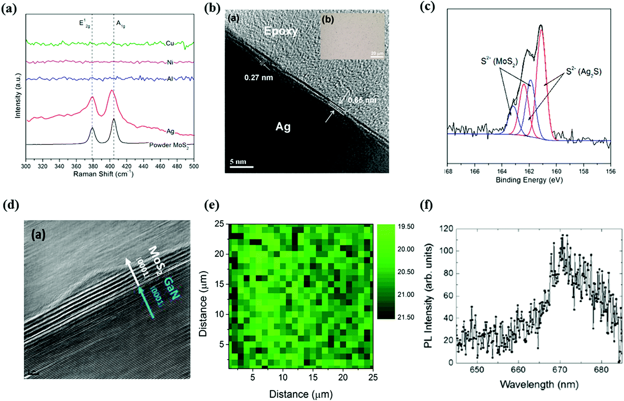 | ||
| Fig. 5 (a) Raman spectra of MoS2 films produced using PLD on various metal substrates. (b) Cross-sectional TEM image of monolayer MoS2 grown on Ag substrate, the inset shows the optical image of the coverage of the film. (c) XPS spectra showing the S 2p core level peaks of Ag supported MoS2. Reproduced with permission of the publishers of ref. 92. Copyright (2014) American Chemical Society. (d) Cross-sectional TEM image of the MoS2 film grown on GaN substrate. Reproduced with permission of the publishers of ref. 94. (e) Raman mapping showing the difference between the A1g and E12g of monolayer MoS2 produced using PLD. (f) PL spectrum of the monolayer MoS2 film grown on a sapphire substrate. Reproduced with permission of the publishers of ref. 96. | ||
Despite the metal substrates, few layer MoS2 films were also realized on several conventional semiconductor/insulator substrates using PLD.94–101 Serrao et al. have employed PLD to grow MoS2 thin films on aluminium oxide (Al2O3) (0001), gallium nitride (GaN) (0001) and silicon carbide-6H (SiC-6H) (0001) substrates.94 To obtain highly crystalline films, tetrathiomolybdate (MoS4) with an optimized stoichiometry was the target, and this resulted in sulfur-rich nanosheets. The growth temperature was 700 °C, which is higher than that used for the growth on metal substrates. The layered structure and high crystallinity of the MoS2 thin films obtained were confirmed using a cross-sectional TEM image (Fig. 5d) and XRD, respectively. In addition, Siegel et al. have successfully grown single layer MoS2 on a sapphire substrate, which was evident using both atomic force microscopy (AFM) images and Raman spectroscopy mapping (Fig. 5e).96 The photoluminescence (PL) results showed that the obtained film had a direct band gap of 1.85 eV (Fig. 5f), which agreed with the characteristic of a monolayer MoS2 nanosheet synthesized using other methods. Recently, highly stoichiometry mono- and few layer MoS2 films were realized on various substrates, [sapphire, hafnium(IV) oxide (HfO2), quartz and SiO2] using PLD.101 MoS2 and S powders with an atomic ratio of 1![[thin space (1/6-em)]](https://www.rsc.org/images/entities/char_2009.gif) :1 were used as precursor materials for the target fabrication. The results of high-resolution Rutherford backscattering confirm the stoichiometry synthesis of MoS2 using PLD. It is important to note that this work reveals that the layer number of MoS2 thin films can be accurately tuned by controlling the number of laser pulses.
:1 were used as precursor materials for the target fabrication. The results of high-resolution Rutherford backscattering confirm the stoichiometry synthesis of MoS2 using PLD. It is important to note that this work reveals that the layer number of MoS2 thin films can be accurately tuned by controlling the number of laser pulses.
4.2 Applications based on PLD-grown MoS2
The previously described few layer MoS2 materials obtained using PLD are found to possess desirable features, such as large scale, good continuity, high uniformity and fewer defects.92–101 All these properties enable the MoS2 films to be applied to a number of electronic and optoelectronic device applications. Late et al. studied the FE and photoresponse of PLD grown MoS2 thin films on various substrates, including tungsten (W) tip, Si wafer and flexible Kapton (polyimide) substrates.102 For the sample of MoS2 grown on the W tip, the SEM image of the film surface exhibited several sharped distributed projections (Fig. 6a), which may work as the intrinsic emitter tips. The FE measurement was conducted on the MoS2/W tip, showing the FE current density of up to 30 mA cm−2 prompted by the voltage of 3.8 kV. The strong FE may be explained by the enhanced local electric field biased to the tip of the projections on the film surface. In addition, good stability of the FE current was observed at 1 μA and no degradation of the emitter's performance was seen after a long measurement time. Whereas for a few layer MoS2 grown on a Si substrate (Fig. 6b), a 1 μA cm−2 emission current density was turned on under the electric field of 2 V μm−1, which is superior to the performance of MoS2 flakes obtained using a liquid method.103 The origin of this low turn-on voltage is ascribed to the nano-scale projections on the MoS2 surface and the good electrical contacts between the thin films and substrates. Furthermore, the authors have measured the UV light photoresponse of a PLD grown MoS2 film on both n and p doped Si substrates.102 When irradiating the sample by 365 nm UV light, large photocurrents were generated, which were induced by the excitons from the interface of MoS2 and the substrates. The rectifying behavior was also recognized from the MoS2/p-Si heterostructure. The similar UV photoresponse was observed from the PLD grown MoS2 thin films supported by the flexible Kapton substrates as well (Fig. 6c).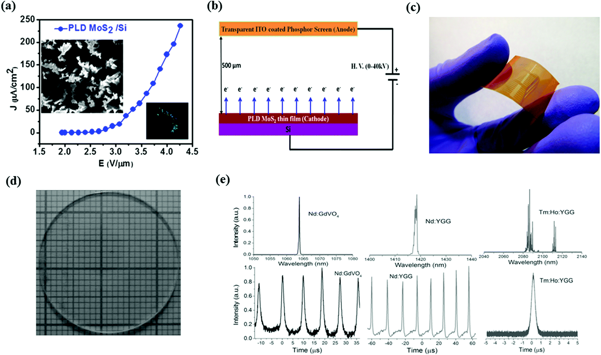 | ||
| Fig. 6 (a) Field emission curve of MoS2 thin films prepared using PLD. The left inset image shows the FESEM image of MoS2 film on a Si substrate, whereas the right inset shows the FE image that was recorded. (b) Schematic of setup used for the FE study of MoS2/Si. (c) Picture of PLD MoS2 film grown on flexible plastic Kapton substrate. Reproduced with permission of the publishers of ref. 102. Copyright (2014), American Chemical Society. (d) Optical image of PLD grown MoS2 on a far UV quartz glass substrate. (e) Typical pulses and laser spectra of the passively Q-switching. Reproduced with permission of publishers of ref. 97. | ||
The PLD grown MoS2 on a UV quartz glass wafer was also developed with a saturable absorber (SA), which exploits the non-linear optical properties of MoS2.97–100 A broadband SA was designed based on several narrow band-gap semiconductors, indicating that the normal MoS2 layers do not satisfy the requirements of this application. To address this issue, PLD was employed to produce MoS2 thin films with S defects, which were induced by the bombardment of the energetic large particles generated from the pulsed laser.97Fig. 6d shows the optical images of PLD grown MoS2 thin film on a far UV quartz glass wafer. It should be noted that the growth temperature is as low as 300 °C. According to the theoretical calculation, the S defects can reduce the band gap of few layers MoS2 from 1.08 eV to 0.08 eV, which makes it applicable for fabricating SA devices. The saturable absorption of the few layer MoS2 obtained was measured by using a picoseconds Nd:YAG laser. The measured saturation intensity is 2.45 GW cm−2 (Fig. 6e), which is superior to that of graphene.104,105 The MoS2 thin films were then employed as the SA for the Q-switched lasers with different wavelengths, which were characterized using a digital oscilloscope. During the measurement, MoS2 layers were not damaged by the heat generated from the pump power, resulting in the stable output while the laser was activated. Consequently, such PLD grown MoS2 shows good saturable absorption properties, which is promising for future SA applications.
4.3 Layered WS2 thin films grown using PLD
As indicated in the literature, wafer scale, few layer WS2 have been deposited on various types of substrates using PLD.106–112 Similar to MoS2, a thin Ag film coated Si wafers were used as substrates for the synthesis of high quality WS2 film, because of the lattice matching Ag2S formation at the interface.107,108 The laser energy was set to 100 mJ and the substrate temperature was kept at 450 °C, which were optimized to obtain a high crystalline and uniform film. Raman spectroscopy (Fig. 7a) and HRTEM images (Fig. 7b) show the layered structure and ultrathin thickness of the WS2 film supported by the Ag2S layer. Interestingly, not only the 2H-WS2 phase, but also the 1T phase of the WS2 nanosheet can be produced. The proportion of 1T-WS2 in this hybrid structure can be tuned by varying the deposition time and strength of laser pulses, which can be explained by the destruction of bonds in 1T-WS2 induced by the high energy atoms and clusters. For the PLD grown WS2 films, it is understandable that the formation of the 1T-phase is attributed to the electron doping induced by the charge transfer from the buffered Ag layer, which has more valence electrons than tungsten, enabling it to act as the electron donor. Therefore, only the WS2 layers near the interface show the metallic 1T phase, which is also proved by the PL measurement (Fig. 7c). In addition, the metastable 1T-WS2 could be transformed to the 2H phase by post annealing at 300 °C, resulting in an improvement in the crystallinity of the hybrid 1T–2H WS2 structure. As 2H and 1T phase WS2 possess a matching lattice structure and compatible contact, the intrinsic semiconductor–metal heterostructure exhibits a chemically uniform layer, which is important for fabricating nano-electronic devices. However, there are problems existing which includes the difficulty of removing the buffer layer without degrading the film, because of the covalent bonds formed between WS2 and the metal sulfide layer. Thus, it should be noted that the Ag2S layer will play an important role for electronic devices based on PLD grown WS2.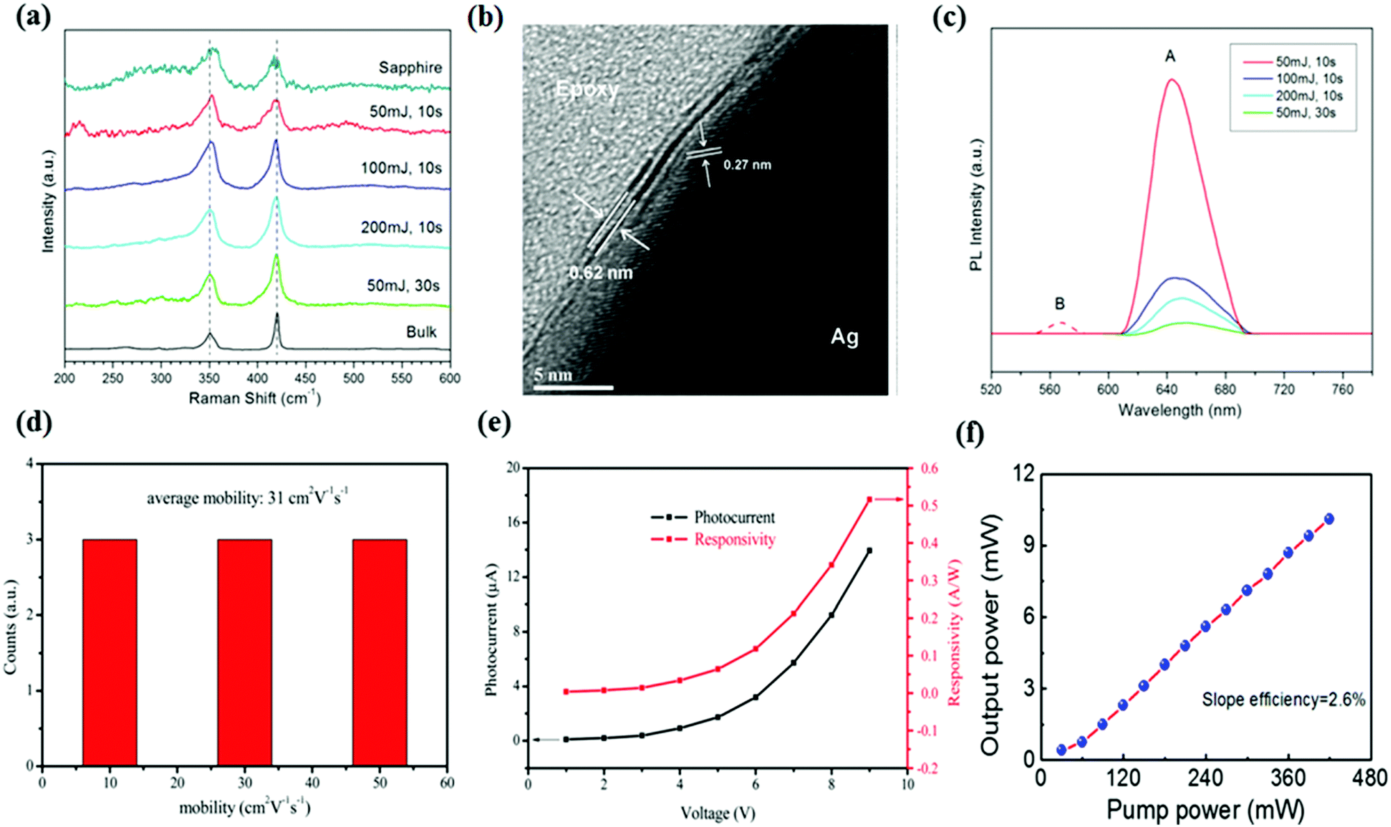 | ||
| Fig. 7 (a) Raman spectra of PLD-grown WS2 films on Ag and sapphire substrates. (b) Cross-sectional TEM image of Ag supported thin films. (c) PL spectra of WS2 thin films grown on Ag substrates. Reproduced with permission of the publishers of ref. 107. (d) The distribution histogram of the Hall mobility. (e) Photocurrent and responsivity versus bias voltage for the WS2 phototransistor in ambient conditions. Reproduced from ref. 110 with permission from The Royal Society of Chemistry. (f) The output power versus the pump power of the dual wavelength soliton pulse based on PLD grown WS2. Reproduced with permission of the publishers of ref. 112. | ||
Instead of employing a metal buffer layer, multi-layer WS2 thin films were directly grown on SiO2 (300 nm)/Si substrates using PLD, and the relevant optoelectronic devices were designed and characterized.110 The growth chamber was maintained in a 50 Pa flowing argon atmosphere. High crystallization and uniformity of the produced WS2 film were characterized using XRD, SEM, AFM and Raman spectroscopy. For the electronic properties, the Hall mobility of the PLD grown WS2 films were measured to be around 31 cm2 V−1 s−1 (Fig. 7d), which is much larger than that of CVD grown films.113 The performance of phototransistors based on PLD WS2 were measured with lasers with a range of wavelength from UV to near-infrared (NIR), which all showed good reproducibility and a large photocurrent, illustrating the broadband photo-detection of the device. The optical responsivity calculated can reach a high value of 0.51 A W−1, which is superior to that obtained for the CVD synthesis WS2 nanosheets (Fig. 7e).110 Until that report was published, this value remained a record for the large scale WS2-based photodetectors, indicating that PLD is a powerful technique to produce high quality WS2 thin films for optoelectronic applications.
As the quantum confinement effect of electron migration and lack of interlayer coupling, the nonlinear optical properties of 2D TMD materials are prominent compared to their bulks.114 Similar to MoS2, PLD grown WS2 was also exploited to be SAs for a dual-wavelength femtosecond soliton mode-locked fiber laser.112 The WS2 thin films were directly deposited onto a fiber taper using laser ablation. By using a 1550 nm pump laser, the saturation intensity and modulation depth of the SA were measured to be 20 MW cm−2 and 0.7%, respectively. The stable dual wavelength oscillation can be observed from the highly erbium-doped fiber laser equipped with PLD grown WS2-based SA. The widths of the laser pulses were 585 fs and 605 fs. As shown in Fig. 7f, the maximum output power of the laser was found to be 10.1 mW with a pulsed laser energy of 1.14 nJ, revealing the excellent performance of the WS2 SA. Table 3 shows a summary of fabrication conditions, quality and optical/electrical properties of PLD-grown TMDs on various substrates. Large scale monolayer MoS2/WS2 thin films can be obtained with proper conditions and experimental setup.
| Growth temperature (°C) | Base pressure (Pa) | Laser energy | Background gases | Morphology | Optical/electrical properties | Ref. | |
|---|---|---|---|---|---|---|---|
| MoS2/stainless steel | RT/200/300/450 | ∼2.66 × 10⁻⁶ | 5 mJ | None | Thick polycrystalline film with a number of large particles on the surface | — | 88 |
| MoS2/Ag | 750 | ∼2.66 × 10⁻⁴ | — | None | <five layers of MoS2 with an average grain size of 600 nm | — | 92 |
| MoS2/W-tip | 700 | 6.65 × 10⁻³ | 2 J cm−2 | ∼1 × 10⁻² mbar Ar | 20–60 nm sized nanocrystals of MoS2 | Emission current = 30 mA cm−2 at 3.8 kV | 102 |
| MoS2/sapphire(0001) | 700 | 1.33 × 10⁻⁴ | 1.5 J cm−2 | None | Centimeter scale monolayer MoS2 with a uniform surface | Direct band gap: 1.85 eV; >90% transmittance above 700 nm | 95 |
| MoS2/Al2O3(0001), GaN(0001), SiC-6H(0001) | 700 | 1.33 × 10⁻⁴ | 50 mJ | 0.1 mTorr residual background | 1–15 layers of MoS2 with roughness of 0.27 nm | Electrical resistivity = 1.6 Ω cm; p-type semiconductor | 94 |
| MoS2/quartz | 300 | 8.9 × 10⁻⁵ | 8.5 J cm−2 | None | ∼30 layers of MoS2 | Broadband absorption; low band gap | 97 |
| WS2/Ag (500 nm)/n-Si | 450 | 2.66 × 10⁻⁴ | 50–200 mJ | None | <five layers of WS2 films | PL peak ∼645 nm, 71% transmittance in the visible range | 106 |
| WS2/SiO2 (300 nm)/Si | 500 | 1 × 10⁻⁴ | — | 50 Pa Ar | Continuous WS2 film with lateral size of one cm | Broad absorbance range from UV to NIR; Hall mobility = 31 cm2 V−1 s−1; photoresponse in air = 0.51 A W−1 | 110 |
5. Hexagonal boron nitrides layers grown using PLD
Born nitride (BN) is the crystalline compound of boron (B) and nitrogen (N) with outstanding chemical and thermal stability, which has been widely used in the high temperature equipment.115 The most stable phase of this material is the h-BN, which has a layered structure similar to graphite.23,116–118 The network of each h-BN layer is composed of B and N atoms bound with strong covalent bonds, whereas the adjacent layers are held by weak vdW forces. The large band gap value (5.97 eV) is induced by the different on-site energies of the B and N atoms. As a typical insulator of 2D layered materials, the dielectric permittivity (ε = 3–4) and breakdown voltage (0.7 V nm−1) of h-BN are superior to those of SiO2, suggesting that the h-BN could be integrated into electronic devices as the dielectric layer.235.1 PLD grown h-BN nanosheets on various substrates
The earlier report on PLD grown h-BN thin film is dated 1999, and the obtained film was used as a buffer layer to improve the adhesion of a cubic boron nitride film (c-BN).119 The synthesis was assisted with the continuous bombardment of N or Ar ions to the substrate, which activated the growth of BN and improved the stoichiometric replication of the film. The obtained h-BN film shows good adhesion and a uniform interface to silicon and stainless steel substrates, respectively. However, the thickness of the synthesized h-BN film was around 100 nm, which is more likely a bulk form rather than an atomically thin 2D material. Therefore, the fabrication and properties characterization of mono- or few layer h-BN still needs further exploration.Recently, ultrathin h-BN films were successfully produced by using a high repetition laser on Mo, aluminum nitride (AIN) and Si substrates.120–125 A high purity pyrolytic h-BN crystal with a boron to nitride atom ratio of 1.05 was used as the target. The growth temperature showed a significant influence on the crystalline structure of BN films, in which the proportion of h-BN increases together with a decrease of the substrate temperature.126–128 One possible reason for this is that the high temperature will increase the internal stress and thermal vibrations of the film, resulting in the phase transition to c-BN. Interestingly, the pure h-BN nanosheets can be obtained at substrate temperature of 450 °C, which is much lower than that of CVD based fabrication. The high uniformity, good crystallinity and high transparency of h-BN films were confirmed using TEM and Raman spectroscopy (Fig. 8a). From the magnified HRTEM image (Fig. 8b), the highly ordered honeycomb structure can be observed and the distance between B and N atoms is about 1.45 Å. The possibility of N–N and B–B bonds can also be excluded. Furthermore, different types of substrate supported h-BN film show a similar structure and morphology. Therefore, the h-BN nanosheets are formed before arriving at the substrate surface, which is evidence that the nanosheets' exfoliation was induced by laser energy from the bulk target. It should be noted that the laser induced high energy particles, molecular or clusters will bring defects and contaminations to the film surface. Sajjad et al. have shown that growth in a hydrogen (H2) environment can effectively reduce the impurities of the h-BN film.122 The interaction between plasma ions and H2 molecules can reduce the energy of particulates in the plasma, which will weaken the side effects of sputtering. Furthermore, the H ions generated from the collision can help to etch the B–O components, resulting in high purity and defect free h-BN films.
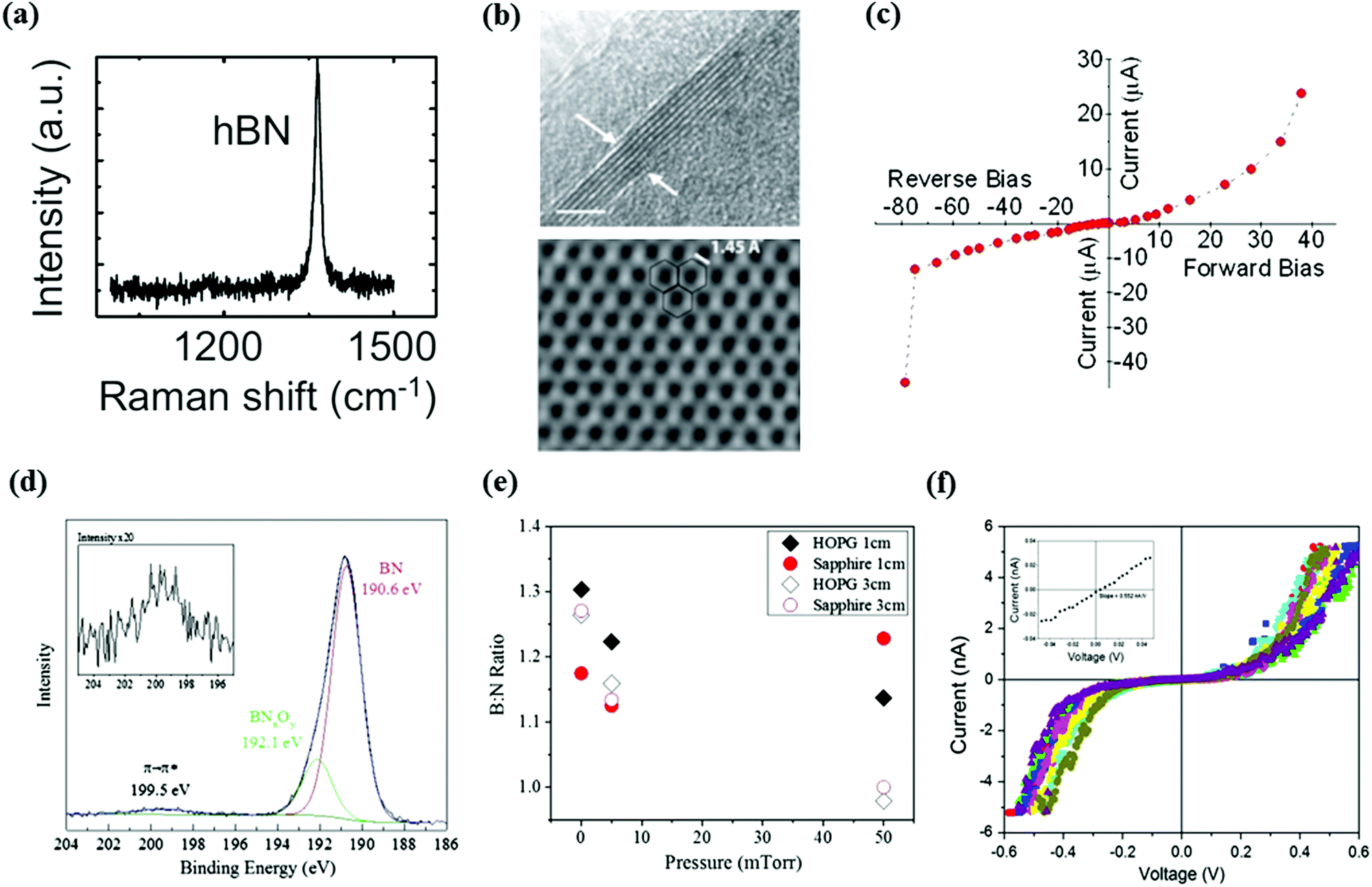 | ||
| Fig. 8 (a) Raman spectrum of h-BN films grown using PLD. (b) Top: Cross-sectional TEM images of h-BN layers. Bottom: HRTEM image showing the honeycomb structure of the h-BN sheet. Reproduced from ref. 120 with permission from Elsevier. (c) Output characteristics of a diode based on h-BN nanosheets. Reproduced with permission of the publishers of ref. 123. (d) XPS scan of the B 1s peak. The inset shows the enlarged satellite peak at the B 1s region. (e) B–N ratio as a function of background pressure for h-BN films grown on different substrates. (f) I–V curves obtained from conducting AFM scans over the PLD grown h-BN film. The average value of the low-biased tunneling curve is shown inset. Reproduced from ref. 129 with permission from Elsevier. | ||
The electrical properties of h-BN nanosheets with few layers were studied using different thicknesses and temperatures, and this revealed that the electrical conductivity of h-BN layers strongly depends on the directions of the measurements, which can be explained by the quantum confinement effect (Fig. 8c). It showed that the electrical resistivity of h-BN sheets decreased together with the decrease of layer numbers when observed from the longitudinal direction, and the ultrathin h-BN presented metal-like properties, which had a large deviation from its bulk. Whereas the measurement temperature was increased from 25 °C to 200 °C, the conductivity of h-BN sheets with few layers was almost fixed along the longitudinal direction. Although the defect free, single crystalline h-BP with few layers were synthesized using PLD, the lateral size of each h-BN nanosheet is only a few micrometers, which resulted in the poor uniformity and morphology over large areas, limiting its applications as a dielectric layer to wafer scale graphene-based devices.
In an alternative study, Glavin et al. reported that the polycrystalline h-BN film was epitaxially grown on HOPG substrate, which had a similar lattice parameter to the h-BN crystal.129,130 In contrast to the previously reported experiment design, an amorphous BN bulk was used as the target in this study, and the growth temperature was raised up to 700 °C. A flowing high purity N2 was introduced as the operation gas, which could strongly affect the composition of the film. The collisions between plasma and background gas result in high concentrations of boron ions and nitrogen. With an optimized target–substrate distance and background pressure, stoichiometric h-BN films possessing high uniformity can be obtained by recombining boron ions and neutral atomic nitrogen. In addition, as the collision with the background gas decelerates the plasma plume, it can help to reduce the kinetic energy of the energetic particulates, which can effectively protect the substrate from the bombardment. The results of XPS (Fig. 8d) and Raman spectroscopy indicated the stoichiometric transfer and epitaxial like growth of h-BN film. As shown in Fig. 8e, with the help of 50 mTorr background N2, the precise replication of chemistry of B:N (1:1) is observed. To characterize the electrical properties of the film obtained, conductive AFM was used. As shown in Fig. 8f, the results show good uniformity of electrical performance for the entire sample over an area of 25 mm2. Therefore, novel 2D electronic devices can be devised from the PLD grown h-BN possessing the highly uniform surface and properties. Very recently, Velázquez et al. have reported the preparation of a monolayer h-BN thin film on strontium titanate (SrTiO3) (001) substrates covered with a 40 nm thick Ag layer.131 The film shows a uniform surface with a large sub-millimeter scale, and can be easily peeled off from the substrates using a mechanical method, which allows for further device characterization without needing a wet transfer process. Table 4 is a summary of h-BN fabrication using PLD, and lists the main deposition conditions and the quality of the as-grown films.
| Growth temperature (°C) | Base pressure (Pa) | Laser energy | Background gases | Morphology | Optical/electrical properties | Ref. | |
|---|---|---|---|---|---|---|---|
| h-BN/Si(100), stainless steel | 365–400 | ∼5 × 10⁻⁵ | 7–20 J cm−2 | 5 × 10⁻² Pa Ar/N2 ions | >6 nm thick h-BN films | — | 119 |
| h-BN/Mo, AlN, quartz | 250–450 | 2 × 10⁻³ | 5 J | None | Average 2.5 nm thick h-BN nanosheets with an average area of ∼2 × m2 | 20 nm thick h-BN nanosheet: ρ = 275 Ω m, breakdown voltage = 1.3 V | 120 |
| h-BN/HOPG, sapphire(0001) | 700 | 1.33 × 10⁻⁵ | 900 mJ | 50 mTorr N2 gas | Large area, six layer h-BN film with a smooth surface | 1.8 nm thick h-BN film: tunneling resistance = 1.811 Ω m−1 | 129 |
| h-BN/Ag(111)/SrTiO3(001) | 400 | 2.66 × 10⁻⁷ | 5–6 J cm−2 | None | 1–10 layers of h-BN | — | 131 |
5.2 Applications based on h-BN grown using PLD
Some device applications from PLD grown h-BN films were realized, including field-effect transistor (FET)132 and deep UV photoconductive detectors.133 With similar crystal structure and good dielectric properties, h-BN is one of the promising substrates for graphene FET.134,135 As reported by Uddin et al., 5 nm thick amorphous BN film was grown on a SiO2/Si substrate using PLD, followed by a post annealing process in a background gas of H2/Ar, which can reduce the dangling bond density and transfer the as-grown film to the required h-BN phase.132 To study the electrical transport properties, graphene prepared using a conventional CVD technique was transferred onto the annealed BN films. The phase of the heterostructure was confirmed using Raman spectroscopy (Fig. 9a). The back-gated transistor based on graphene/h-BN was characterized and showed a three-fold higher carrier mobility compared to that of a graphene/SiO2/Si transistor at room temperature (RT; Fig. 9b). For 35 device measurements, the maximum hole and electron mobility obtained were 4980 and 4200 cm2 V−1 s−1, respectively (Fig. 9c), which are superior to those of transistors based on graphene and h-BN grown using CVD.134 The residual carrier concentration and average Dirac point of graphene/h-BN were reduced to one-tenth of those values of graphene transistors supported by SiO2, illustrating that the extrinsic doping and the charge inhomogeneity of graphene are largely decreased. Such a good electronic performance may have resulted from the diminution of the charged impurity induced Coulomb scattering and the larger phonon energy of h-BN.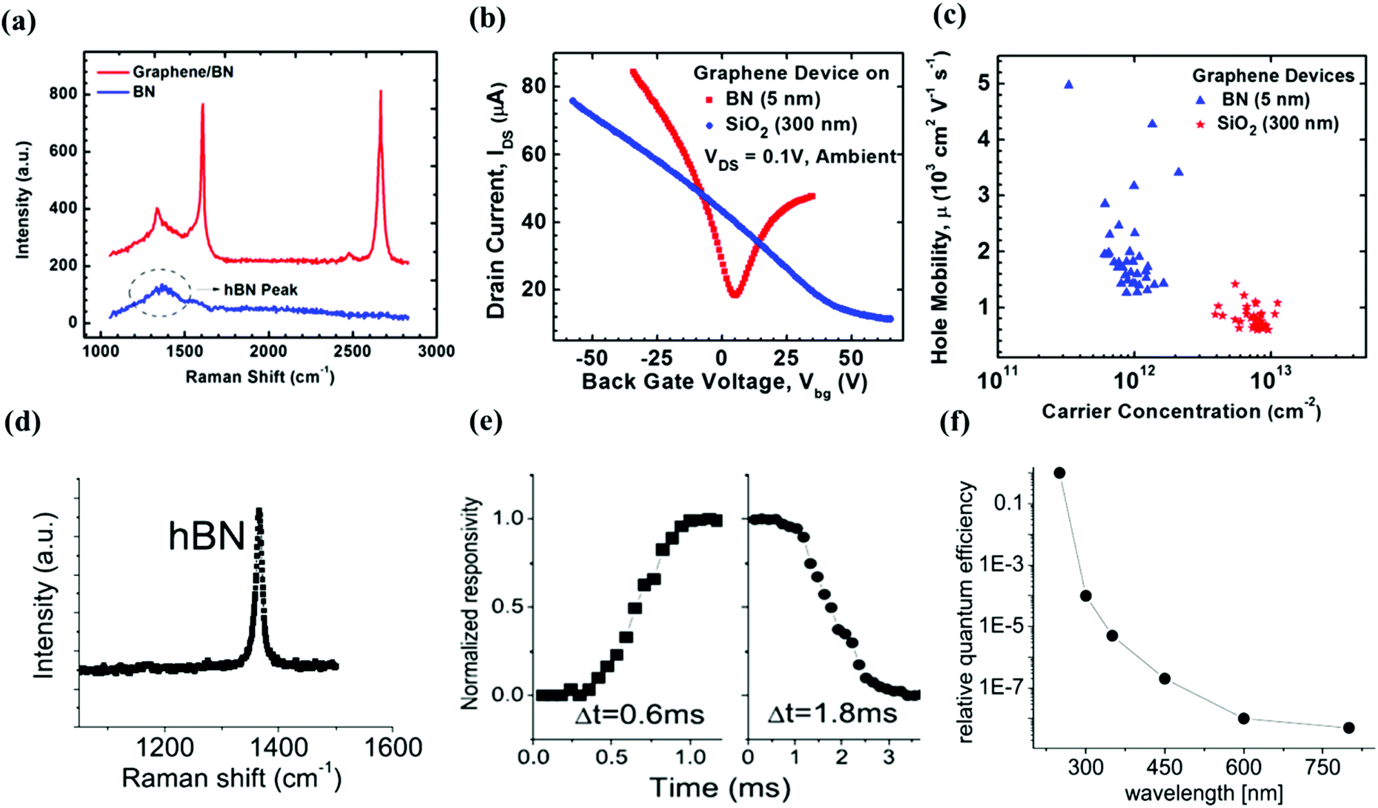 | ||
| Fig. 9 (a) Raman spectra of graphene/h-BN heterostructure and h-BN. (b) Transfer characteristics of graphene transistors on h-BN (red line) and SiO2/Si (blue) substrates. (c) Relationship between hole mobility of a graphene FET and the corresponding carrier concentration of graphene grown on 5 nm h-BN (blue triangle) and 300 nm SiO2 (red star) substrates. Reproduced with permission of the publishers of ref. 132. (d) Raman spectrum of h-BN grown using PLD. (e) The relationship between responsivity and time of a photodetector based on h-BN nanosheets. (f) The curve of relative quantum efficiency and the detected wavelength. Reproduced with permission of the publishers of ref. 133. | ||
Besides its use as a gate insulator for graphene-based transistors, h-BN is one of the desirable materials for fabricating into a UV detector because of its large band gap and good optical properties. Aldalbahi and Feng developed and characterized a high performance UV detector based on the 2D h-BN nanosheets deposited using PLD.133 The highly crystalline and defect free layered structure of h-BN sheets were characterised using Raman spectroscopy (Fig. 9d), SEM and TEM. The characterization of the UV photodetector showed that the response time was as short as 0.6 ms (Fig. 9e). The performance of the h-BN-based photodetector was highly influenced by the ambient temperature because of the thermal noise. When the processing temperature is above 200 °C, the device cannot detect the signal with an intensity of less than 0.1 mW. Based on the result, it can be concluded that the photodetector based on the PLD grown h-BN film is very sensitive to light in the UV region. However, as shown in Fig. 9f, for light with a longer wavelength, the relative quantum efficiency is largely attenuated.
6. Layered GaSe nanoflakes fabricated using PLD
Among the layered metal chalcogenides, 2D GaSe has received much attention from researchers in various fields of electronics, optoelectronics, and nonlinear optics because of its p-type semiconductor nature, wide band gap value of around 2.0 eV and desirable nonlinear response.136,137 For example, Jie et al. first observed layer dependent nonlinear optical properties in 2D GaSe material.138 GaSe with few layers has a hexagonal structure with stacks of repeating covalent bonded Se–Ga–Ga–Se layers, with a lattice constant of 0.374 nm and D3h symmetry. Up to now, use of mechanical exfoliation,139 molecular beam epitaxy (MBE)140 and CVD141 techniques have been used to realize mono- and few layer GaSe flakes. Compared with these techniques, PLD is a simple method for fabricating high quality thin films with accurately controllable thickness and low processing temperature. Recently, Mahjouri-Samani et al. reported that GaSe nanosheets with a few layers were achieved on SiO2 (300 nm)/Si substrates using PLD.142 It was found that the size, density, morphology, thickness and crystal structure of the 2D GaSe crystals were determined by the growth temperature, fabrication duration, base pressure and laser fluence. To obtain the high uniformity and precise stoichiometry thin films, a background inert gas (∼1 Torr Ar) was introduced to the fabrication process, which could balance the kinetic energies of the ejected precursor plasma to benefit the nucleation of the triangular GaSe nanosheets. The flowing Ar gas at an appropriate pressure will promote the formation of GaSe nanosheets by confining the plasma plume. Nevertheless, higher Ar pressures (>5 Torr) will generate larger aggregated clusters that may be detrimental to the formation of GaSe layers. According to the HRTEM images (Fig. 10a), δ- or ε-type GaSe was obtained and the single crystalline structure with perfect stacking of GaSe layers can also be observed. The morphology and thickness of the GaSe nanosheets obtained were characterized using SEM, AFM and Raman spectroscopy (Fig. 10b), showing that individual 1–3 layer, random oriented triangular GaSe flakes with a lateral scale of around 200 nm were produced under low laser pulses. Together with the increase in deposition time, the continuous film was formed by the accumulation of new nanosheets, revealing a layer-by-layer like growth strategy. The electrical properties were characterized by fabricating FET based on a PLD grown GaSe nanosheet with 20 layers. A p-type transistor feature can be observed from the transfer characteristic curve, and the FE carrier mobility and current switching ratio were measured to be 0.1 cm2 V−1 s−1 and 104, respectively, which is comparable to the same measurements obtained for GaSe thin sheets obtained using mechanical exfoliation.143 The optoelectronic performance of the GaSe-based transistor was also characterized. The photo responsivity of the device was measured in a range of 0.4–1.4 AW−1 when illuminated with a 700 nm to 240 nm light source (Fig. 10c), which is superior to the responsivity of a phototransistor based on PLD grown WS2 thin films (0.51 AW−1) and comparable to that of the mechanical exfoliated GaSe flakes.143 Based on the spectral responsivity value, the corresponding external quantum efficiency (EQE) can be calculated to range from 100% at 700 nm to 600% at 240 nm. These high spectral responsivities are ascribed to the midgap states induced by the grain boundaries from the polycrystallinity of the PLD grown GaSe films.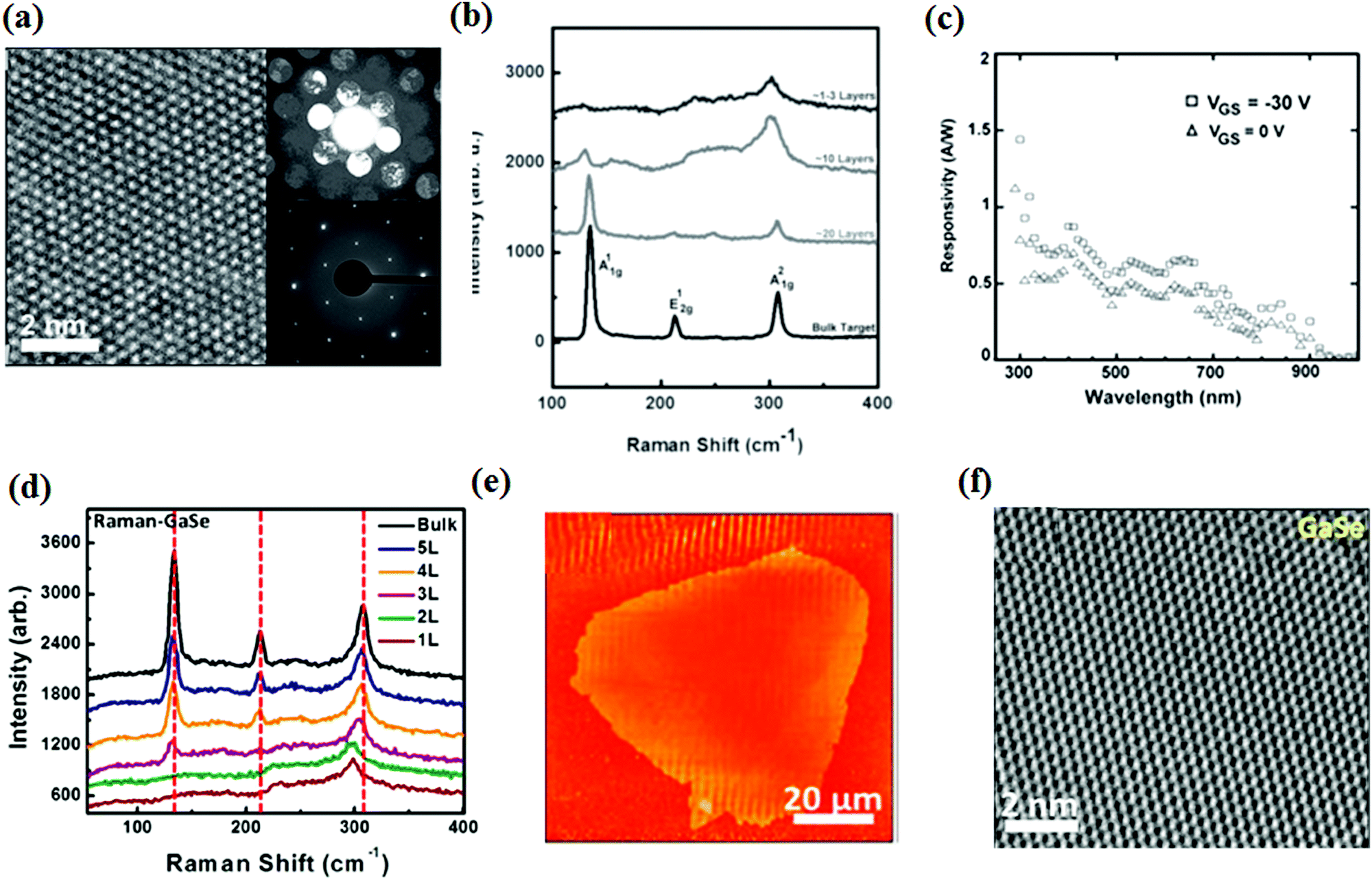 | ||
| Fig. 10 (a) HRTEM image of a GaSe nanosheet, bottom inset shows the results of SAED patterns, top inset shows the nano-beam diffraction patterns. (b) Raman spectra of GaSe nanosheets of different thickness. (c) Photoresponsivity at VGS = −30 V and VGS = 0 V of GaSe nanosheets as a function of selected wavelengths of incident monochromatic light. Reproduced with permission of the publishers of ref. 142. (d) Raman spectra of GaSe nanosheets with a different number of layers. (e) AFM image of a large monolayer GaSe sheet. (f) HRTEM image of GaSe nanosheets. Reproduced with permission of the publishers of ref. 144. Copyright (2014), American Chemical Society. | ||
Although the stoichiometry transferred and uniform 2D GaSe nanosheets were successfully produced using PLD, the average small scale (∼200 nm) of the obtained triangular sheets caused by the high nucleation density hinders its real applications. To synthesize continuous layered GaSe thin films at the wafer scale, Mahjouri-Samani et al. developed a new hybrid growth technique, which combines PLD and vapor transport growth (VTG) methods, one of the popular techniques for depositing large-scale single crystal nanosheets of layered metal chalcogenides.144 This novel technique has the advantages of both PLD and VTG, which might result in the films with accurate replication of the stoichiometry, high nucleation density, and large crystalline domains. As the first step of this method, GaSe nanosheets were grown using PLD on top of SiO2 (300 nm)/Si substrates, as the source substrate in this experiment. To guarantee the good stoichiometric transfer of the thin films, a background Ar gas (∼1 Torr) was exploited and the laser fluence was set at 1 J cm−2. The morphology of the obtained GaSe film was mainly a large amount of nanoparticles, which were detected using the low-resolution transmission electron microscopy (LRTEM). The second step is to attach the GaSe thin film on to the surface of a new Si substrate, which is called the receiver substrate, to form a confined fabrication situation. This combined structure was heated up in an environment of 10–20 Torr background Ar gas, resulting in a temperature gradient for initiating growth. The growth temperature was set to be capable of evaporating the GaSe nanoparticles onto the receiver substrate and growth of 2D layers. A continuous monolayer GaSe film with a typical triangular appearance was confirmed from Raman spectroscopy (Fig. 10d) and AFM images (Fig. 10e). The maximum lateral size of the continuous film obtained can be up to 0.5 mm2, which is much larger than that of GaSe nanosheets grown using simple PLD. By further increasing the number of laser pulses, the individual nanosheets formed will merge into a larger and thicker continuous film as exhibited in the AFM image. Furthermore, the single crystalline, hexagonal lattice structure of the GaSe film obtained was measured using HRTEM and selected area electron diffraction (SAED; Fig. 10f). The PLD-VTG technique was also used to synthesize large-scale monolayer MoSe2,144,145 indicating that this method is promising for fabricating a variety of binary and ternary 2D metal chalcogenide thin films.
7. Black phosphorus ultrathin films produced using PLD
As the most thermodynamically stable allotrope of phosphorus, BP was first synthesized from white phosphorus under high pressure in 1914.146 Similar to graphite, BP has a puckered layer structure, with vdW interactions between adjacent layers. Although various properties of its bulk form have been investigated for over 100 years, there have been only a few studies for applying BP for useful device applications until the year of 2014, and this is partially attributed to an obstacle in fabrication. In 2014, Li et al. in Fudan, China and Liu et al. in Purdue, USA have done pioneer work on atomically thin BP, called phosphorene which can be isolated by peeling it off from the bulk form.17,18 The discovery of BP has ignited the research interest of the scientists because of BP's unexpected properties compared with its bulk counterpart.17–19 Combining the advantages of both graphene and MoS2, phosphorene exhibits a high carrier mobility and a direct intrinsic band gap (0.3–2 eV), which can be tuned by the layer number. In addition, because of the low spin–orbit coupling, BP with few layers is also desirable for investigating spin transport.147Until now, phosphorene can only be obtained by top-down methods, namely mechanical exfoliation and solution-based exfoliation, which only provides the small sized flakes. Because of the chemically active surface of ultrathin BP flakes, the chemically based bottom-up method has not yet been realized to produce scalable BP films. Recently, PLD has been used to grow the wafer scale BP-based ultrathin films with a highly disordered structure, called amorphous black phosphorus (a-BP), on both graphene/Cu and SiO2/Si substrates.148 The a-BP thin films were deposited at processing temperature of ∼150 °C, which is in contrast with the harsh conditions required to synthesize BP bulk crystal.146 Similar to phosphorene, a-BP thin films show the thickness dependent direct band gap. The chemical composition and structure were characterized using energy-dispersive X-ray spectroscopy (EDX) and Raman spectroscopy (Fig. 11a and b). More importantly, the FET measurement shows that the as-grown a-BP thin films show a p-type behavior and high hole mobility up to 100 cm2 V−1 s−1 (Fig. 11c), which is superior to that of other commonly used elemental amorphous semiconductor thin films, such amorphous silicon (a-Si),149 amorphous carbon (a-C)150 or amorphous germanium (a-Ge).151 Interestingly, as shown in Fig. 11d, the observed thickness dependent FE mobility and switching ratio of the a-BP channel is similar to the performance of phosphorene-based transistors. Because the large scale film and low processing temperature are beneficial for device applications, it is expected that such PLD grown a-BP thin films will scientifically and technologically have more attention in the future.
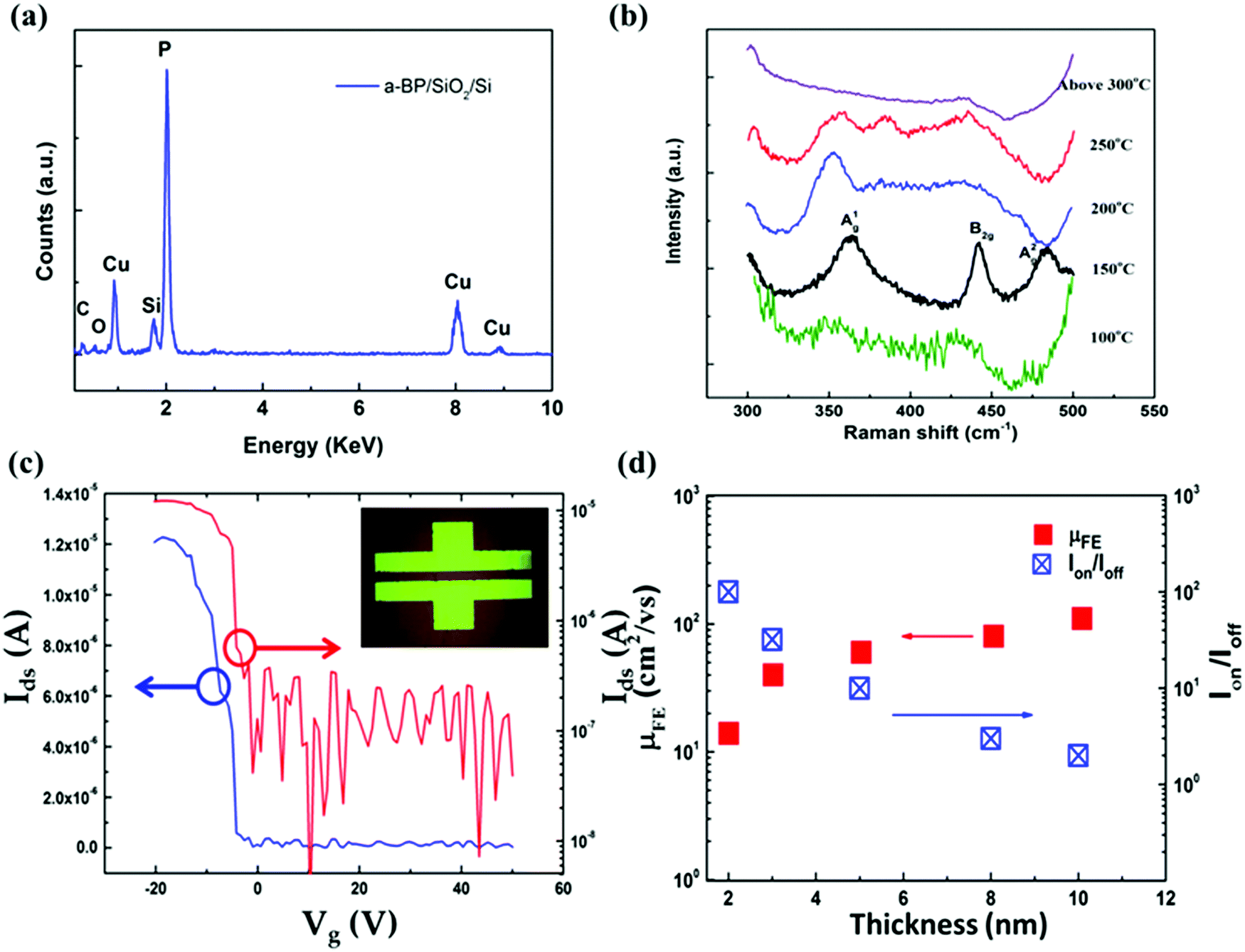 | ||
| Fig. 11 (a) EDX spectrum of a-BP film grown on SiO2/Si. (b) Raman spectra of a-BP films deposited under different temperatures. (c) Transfer characteristics of an a-BP transistor. The inset shows the optical image of the electrode pattern used for the measurement. (d) The mobility and on/off ratio of the BP FET as a function of the thickness. Reproduced with permission of the publishers of ref. 148. | ||
8. Conclusions and outlook
The burst of studies on 2D materials have aroused great interest in characterising the novel physical and chemical properties of the materials. In order to achieve the objective of applying these ultrathin materials to practical applications, the desirable samples should have a wafer scale with uniform morphology and the material properties required for the devices. Furthermore, it is required that the fabrication technology can provide a scale up process with acceptable throughput and easy growth conditions. The technique of PLD is appealing for the growth of 2D materials as an alternative to conventional CVD. As far as is known, this is the first review article on this emerging research field. The primary goal of this review is to systematically present an overview of experimental synthesis, characterization, and potential device applications of several typical 2D materials deposited using PLD. Previous studies indicate that main groups of 2D materials (graphene, TMDs, h-BN and GaSe) and a-BP thin films can be grown using PLD. The wafer scale layered films show high crystallinity, good adhesion and accurate replication of the material's stoichiometry, depending on the specific growth conditions, such as substrate temperature, energy density of irradiated laser on the target, background pressure and so on. Traditionally, PLD is considered as a technique for depositing conventional thin films, from mainly oxide-based compounds. Therefore, the successful growth of 2D layered materials can be regarded as broadening application scope of PLD from traditional thin film to a new platform of 2D materials. Compared to the atomically thin layers obtained by other commonly used methods, such as mechanical exfoliation, chemical and liquid exfoliation, CVD and so on, the 2D thin films prepared using PLD show the merits of good adhesion with substrates, accurate replication of stoichiometry, fast growth speed and relatively low fabrication temperature. With these features of PLD grown 2D materials, some novel 2D devices have been conceived and fabricated during the past few years. The performances of typical 2D devices, including transistors, photodetectors and SAs, are reviewed. Compared with the extensive studies on CVD grown 2D materials, it seems that the investigations on the synthesis of atomically thin layered materials using PLD have only just started. Some challenges and opportunities that exist are:(i) The fundamental processes of PLD grown 2D layers, particularly occurring within the laser produced plasmas, are not fully understood. Therefore, the growth of new 2D materials usually needs a relatively long period to optimize the deposition conditions. The problem might be addressed by combining the growth experiments with construction of applicable simulation models of PLD growth for 2D materials. Some simulations have been reported for the CVD growth of 2D materials.152 Unfortunately, there is the lack of such a model for PLD grown 2D materials at this moment.
(ii) As previously introduced in the large scale GaSe fabrication, the hybrid techniques combining PLD with other bottom-up methods (CVD or MBE) can be considered to further improve the quality of the films and overcome some shortcomings of PLD, such as the thickness inhomogeneity, limited scale and poor continuity. This approach may provide new opportunities for PLD in the synthesis of high quality 2D materials.
(iii) Up to now, the members of the 2D material family have been extended to several hundred. However, the types of materials already attempted to be grown using PLD are very limited compared to the large number of members of the 2D material family. According to the literature review, some 2D materials are not easy to produce using either CVD technique or mechanical/liquid exfoliation; examples include the chemically active materials, e.g., silicene, or materials with a strong interlayer bonding, e.g., MXenes. Obviously, it is worth exploring the PLD growth for more types of 2D materials.
(iv) It is feasible to implement a doping strategy during the fabrication process of PLD grown 2D materials, which has not yet been attempted. The potential methods may include either intermingling the dopants to the target materials, or mixing the dopants into the background gases. Therefore, it could be a promising research direction to study the doping effects on the PLD grown 2D films in the future.
Lastly, 2D vdW based heterostructures have recently shown great promise for both fundamental study and constructing a wide range of electronic and optoelectronic devices.153–156 In the past, PLD has proven to be a powerful tool not only in depositing a single layer of thin film, but also in in situ fabricating heterostructures via sequentially rotating different targets without breaking the vacuum. Accordingly, it is believed that PLD will play an important role in making various 2D based heterostructures for device applications in the future.
Acknowledgements
The research was supported by the grants from Research Grants Council of Hong Kong (GRF No. PolyU 153031/15P), National Natural Science Foundation of China (Grant No. 11474241), and Collaborative Research Fund (CRF No. HKU9/CRF/13G, PolyU Grant No. E-RD5), and PolyU Internal Grant (4-BCAG).References
- G. E. Moore, Electronics, 1965, 38, 114 Search PubMed.
- G. E. Moore, IEEE IEDM Tech. Dig., 1975, 21, 11 Search PubMed.
- C. Tourney, Nat. Nanotechnol., 2016, 11, 2 CrossRef PubMed.
- M. M. Waldrop, Nature, 2016, 530, 144 CrossRef CAS PubMed.
- S. E. Thompson and S. Parthasarathy, Mater. Today, 2006, 9, 20 CrossRef CAS.
- S. Ornes, Proc. Natl. Acad. Sci. U. S. A., 2015, 112, 13128 CrossRef CAS PubMed.
- K. S. Novoselov, A. K. Geim, S. Morozov, D. Jiang, Y. Zhang, S. V. Dubonos, I. V. Grigorieva and A. A. Firsov, Science, 2004, 306, 666 CrossRef CAS PubMed.
- K. Novoselov, A. Geim, S. Morozov, D. Jiang, M. Katsnelson, I. Grigorieva, S. Dubonos and A. Firsov, Nature, 2005, 438, 197 CrossRef CAS PubMed.
- D. Akinwande, P. Nicholas and H. James, Nat. Commun., 2014, 5, 5678 CrossRef CAS PubMed.
- Z. S. Butler, S. M. Hollen and L. Y. Cao, ACS Nano, 2013, 7, 2898 CrossRef PubMed.
- A. K. Geim and K. S. Novoselov, Nat. Mater., 2007, 6, 183 CrossRef CAS PubMed.
- C. Lee, X. Wei, J. W. Kysar and J. Hone, Science, 2008, 321, 385 CrossRef CAS PubMed.
- D. Sun, G. Aivazian, A. M. Jones, J. S. Ross, W. Yao, D. Cobden and X. Xu, Nat. Nanotechnol., 2012, 7, 114 CrossRef CAS PubMed.
- Q. H. Wang, K. Kalantar-Zadeh, A. Kis, J. N. Coleman and M. S. Strano, Nat. Nanotechnol., 2012, 7, 699 CrossRef CAS PubMed.
- O. N. Weiss, H. Zhou, L. Liao, Y. Liu, S. Jiang, Y. Huan and X. Duan, Adv. Mater., 2012, 24, 5782 CrossRef PubMed.
- B. Radisavljevic, A. Radenovic, J. Brivio, V. Giacometti and A. Kis, Nat. Nanotechnol., 2011, 6, 147 CrossRef CAS PubMed.
- L. Li, Y. Yu, G. J. Ye, Q. Ge, X. Ou, H. Wu, D. Feng, X. H. Chen and Y. Zhang, Nat. Nanotechnol., 2014, 9, 372 CrossRef CAS PubMed.
- H. Liu, A. T. Neal, Z. Zhu, Z. Luo, X. Xu, D. Tománek and P. D. Ye, ACS Nano, 2014, 8, 4033 CrossRef CAS PubMed.
- F. Xia, H. Wang and Y. Jia, Nat. Commun., 2014, 5, 4458 CAS.
- L. Tao, E. Cinquanta, D. Chiappe, C. Grazianetti, M. Fanciulli, M. Dubey, A. Molle and D. Akinwande, Nat. Nanotechnol., 2015, 10, 227 CrossRef CAS PubMed.
- P. Vogt, P. D. Padava, C. Quaresima, J. Avila, E. Frantzeskakis, M. C. Asensio, A. Resta, B. Ealet and G. L. Lay, Phys. Rev. Lett., 2012, 108, 155501 CrossRef PubMed.
- A. Pakdel, Y. Bando and D. Golbery, Chem. Soc. Rev., 2014, 43, 934 RSC.
- Y. Kubota, K. Watanabe, O. Tsuda and T. Taniguchi, Science, 2007, 317, 932 CrossRef CAS PubMed.
- P. Miró, M. Audiffred and T. Heine, Chem. Soc. Rev., 2014, 43, 6537 RSC.
- A. C. Ferrari, F. Bonaccorso, V. Fal’ko, K. S. Novoselov, S. Roche, P. Bøggild, S. Borini, F. H. L. Koppens, V. Palermo, N. Pugno, J. A. Garrido, R. Sordan, A. Bianco, L. Ballerini, M. Prato, E. Lidorikis, J. Kivioja, C. Marinelli, T. Ryhänen, A. Morpurgo, J. N. Coleman, V. Nicolosi, L. Colombo, A. Fert, M. Garcia-Hernandez, A. Bachtold, G. F. Schneider, F. Guinea, C. Dekker, M. Barbone, Z. Sun, C. Galiotis, A. N. Grigorenko, G. Konstantatos, A. Kis, M. Katsnelson, L. Vandersypen, A. Loiseau, V. Morandi, D. Neumaier, E. Treossi, V. Pellegrini, M. Polini, A. Tredicucci, G. M. Williams, B. H. Hong, J.-H. Ahn, J. M. Kim, H. Zirath, B. J. van Wees, H. van der Zant, L. Occhipinti, A. D. Matteo, I. A. Kinloch, T. Seyller, E. Quesnel, X. Feng, K. Teo, N. Rupesinghe, P. Hakonen, S. R. T. Neil, Q. Tannock, T. Löfwander and J. Kinaret, Nanoscale, 2015, 7, 4598 RSC.
- P. Avouris, Z. Chen and V. Perebeinos, Nat. Nanotechnol., 2007, 2, 605 CrossRef CAS PubMed.
- D. Xiao, G.-B. Liu, W. Feng, X. Xu and W. Yao, Phys. Rev. Lett., 2012, 108, 196802 CrossRef PubMed.
- L. Britnell, R. V. Gorbachev, R. Jalil, B. D. Belle, F. Schedin, A. Mishchenko, T. Georgiou, M. I. Katsnelson, L. Eaves, S. V. Morozov, N. M. R. Peres, J. Leist, A. K. Geim, K. S. Novoselov and L. A. Ponomarenko, Science, 2012, 335, 947 CrossRef CAS PubMed.
- Y. Shi, H. Li and L.-J. Li, Chem. Soc. Rev., 2015, 44, 2744 RSC.
- Q. Ji, Y. Zhang, Y. Zhang and Z. Liu, Chem. Soc. Rev., 2015, 44, 2587 RSC.
- C. Mattevi, H. Kim and M. Chhowalla, J. Mater. Chem., 2011, 21, 3324 RSC.
- H. F. Liu, S. L. Wong and D. Z. Chi, Chem. Vap. Deposition, 2015, 21, 241 CrossRef CAS.
- B. Roas, L. Schultz and G. Endres, Appl. Phys. Lett., 1988, 53, 1557 CrossRef CAS.
- J. H. Hao, Y. Zhang and X. H. Wei, Angew. Chem., 2011, 123, 7008 CrossRef.
- I. A. Akimov, A. A. Sirenko, A. M. Clark, J. H. Hao and X. X. Xi, Phys. Rev. Lett., 2000, 84, 4625 CrossRef CAS PubMed.
- G. X. Bai, Y. Zhang and J. H. Hao, Sci. Rep., 2014, 4, 5724 CAS.
- Y. Zhang and J. H. Hao, J. Appl. Phys., 2013, 113, 184112 CrossRef.
- Z. B. Yang and J. H. Hao, J. Appl. Phys., 2012, 112, 054110 CrossRef.
- Y. Zhang, G. Y. Gao, H. L. W. Chan, J. Y. Dai, Y. Wang and J. H. Hao, Adv. Mater., 2012, 24, 1729 CrossRef CAS PubMed.
- J. H. Hao, W. D. Si, X. X. Xi, R. Guo, A. S. Bhalla and L. E. Cross, Appl. Phys. Lett., 2000, 76, 3100 CrossRef CAS.
- Z. B. Yang, W. Huang and J. H. Hao, Appl. Phys. Lett., 2013, 103, 031919 CrossRef.
- W. Huang, J. Y. Dai and J. H. Hao, Appl. Phys. Lett., 2010, 97, 162905 CrossRef.
- W. Huang, Z. P. Wu and J. H. Hao, Appl. Phys. Lett., 2009, 94, 032905 CrossRef.
- J. H. Hao, J. Gao, Z. Wang and D. P. Yu, Appl. Phys. Lett., 2005, 87, 131908 CrossRef.
- K. Nomura, H. Ohta, A. Takagi, T. Kamiya, M. Hirano and H. Hosono, Nature, 2004, 432, 488 CrossRef CAS PubMed.
- W. Hoheisel, K. Jungmann, M. Vollmer, R. Weidenauer and F. Träger, Phys. Rev. Lett., 1988, 60, 1649 CrossRef CAS PubMed.
- D. J. Krajnovich, J. E. Vázquez and R. J. Savoy, Science, 1993, 259, 1590 CAS.
- S. Amoruso, G. Ausanio, C. de Lisio, V. Iannotti, M. Vitiello, X. Wang and L. Lanotte, Appl. Surf. Sci., 2005, 247, 71 CrossRef CAS.
- B. Holzapfel, B. Roas, L. Schultz, P. Bauer and G. Saemann-Ischenko, Appl. Phys. Lett., 1992, 61, 3178 CrossRef CAS.
- Z. Trajanovic, S. Choopun, R. P. Sharma and T. Venkatesan, Appl. Phys. Lett., 1997, 70, 3461 CrossRef.
- H. L. Spindler, R. M. Gilgenbach and J. S. Lash, Appl. Phys. Lett., 1996, 68, 3245 CrossRef CAS.
- Z. Liu, S. P. Lau and F. Yan, Chem. Soc. Rev., 2015, 44, 5638 RSC.
- H. Zeng, J. Dai, W. Yao, D. Xiao and X. Cui, Nat. Nanotechnol., 2012, 7, 490 CrossRef CAS PubMed.
- M. Buscema, D. J. Groenendijk, G. A. Steele, H. S. J. van der Zant and A. Castellanos-Gomez, Nat. Commun., 2014, 5, 4651 CrossRef CAS PubMed.
- C. Lee, H. Yan, L. E. Brus, T. F. Heinz, J. Hone and S. Ryu, ACS Nano, 2010, 4, 2695 CrossRef CAS PubMed.
- L. J. Cote, F. Kim and J. Huang, J. Am. Chem. Soc., 2008, 131, 1043 CrossRef PubMed.
- M. Chhowalla, H. S. Shin, G. Eda, L.-J. Li, K. P. Loh and H. Zhang, Nat. Chem., 2013, 5, 263 CrossRef PubMed.
- L. Tang, R. Ji, X. Li, G. Bai, C. P. Liu, J. Hao, J. Lin, H. Jiang, K. S. Teng, Z. Yang and S. P. Lau, ACS Nano, 2014, 8, 6312 CrossRef CAS PubMed.
- S. Lin, S. Liu, Z. Yang, Y. Li, T. W. Ng, Z. Xu, Q. Bao, J. Hao, C.-S. Lee, C. Surya, F. Yan and S. P. Lau, Adv. Funct. Mater., 2016, 26, 864 CrossRef CAS.
- G. Bai, S. Yuan, Y. Zhao, Z. Yang, S. Y. Choi, Y. Chai, S. F. Yu, S. P. Lau and J. Hao, Adv. Mater., 2016, 28, 7472 CrossRef CAS PubMed.
- W. Jie, F. Zheng and J. Hao, Appl. Phys. Lett., 2013, 103, 233111 CrossRef.
- J. Deng, R. Zheng, Y. Zhao and G. Cheng, ACS Nano, 2012, 6, 3727 CrossRef CAS PubMed.
- C. Gong, C. Huang, J. Miller, L. Cheng, Y. Hao, D. Cobden, J. Kim, R. S. Ruoff, R. M. Wallace, K. Cho, X. Xu and Y. J. Chabal, ACS Nano, 2013, 7, 11350 CrossRef CAS PubMed.
- Q. Feng, Y. Zhu, J. Hong, M. Zhang, W. Duan, N. Mao, J. Wu, H. Xu, F. Dong, F. Lin, C. Jin, C. Wang, J. Zhang and L. Xie, Adv. Mater., 2014, 26, 2648 CrossRef CAS PubMed.
- E. Cappelli, S. Lacobucci, C. Scilletta, R. Flammini, S. Orlando, G. Mattei, P. Ascarelli, F. Borgatti, A. Giglia, N. Mahne and S. Nannarone, Diamond Relat. Mater., 2005, 14, 959 CrossRef CAS.
- C. Scilletta, M. Servidori, S. Orlando, E. Cappelli, L. Barba and P. Ascarelli, Appl. Surf. Sci., 2006, 252, 4877 CrossRef CAS.
- E. Cappelli, S. Orlando, M. Servidori and C. Scilletta, Appl. Surf. Sci., 2007, 254, 1273 CrossRef CAS.
- J. Coraux, A. T. N’diaye, C. Busse and T. Michely, Nano Lett., 2008, 8, 565 CrossRef CAS PubMed.
- A. T. T. Koh, Y. M. Foong and D. H. C. Chua, Appl. Phys. Lett., 2010, 97, 114102 CrossRef.
- K. Wang, G. Tai, K. H. Wong, S. P. Lau and W. Guo, AIP Adv., 2011, 1, 022141 CrossRef.
- A. T. T. Koh, Y. M. Foong and D. H. C. Chua, Diamond Relat. Mater., 2012, 25, 98 CrossRef CAS.
- G. K. Hemani, W. G. Vandenberghe, B. Brennan, Y. J. Chabal, A. V. Walker, R. M. Wallace, M. Quevedo-Lopez and M. V. Fischetti, Appl. Phys. Lett., 2013, 103, 134102 CrossRef.
- V. Kaushik, H. Sharma, A. K. Shukla and V. D. Vankar, Vacuum, 2014, 110, 1 CrossRef CAS.
- J. Wang, Z. Xiong, J. Yu, H. Yin, X. Wang, L. Peng, Y. Wang, X. Wang, T. Jiang, L. Cao, W. Wu, C. Wang and L. Zhang, Micro Nano Lett., 2015, 10, 649 Search PubMed.
- P. Fortgang, T. Tite, V. Barnier, N. Zehani, C. Maddi, F. Lagarde, A.-S. Loir, N. Jaffrezic-Renault, C. Donnet, F. Garrelie and C. Chaix, ACS Appl. Mater. Interfaces, 2016, 8, 1424 CAS.
- M. Qian, Y. S. Zhou, Y. Gao, J. B. Park, T. Feng, S. M. Huang, Z. Sun, L. Jiang and Y. F. Lu, Appl. Phys. Lett., 2011, 98, 173108 CrossRef.
- M. Reininghaus, D. Wortmann, J. Finger, O. Faley, R. Poprawe and C. Stampfer, Appl. Phys. Lett., 2012, 100, 151606 CrossRef.
- S. R. Sarath Kumar and H. N. Alshareef, Appl. Phys. Lett., 2013, 102, 012110 CrossRef.
- I. Kumar and A. Khare, Appl. Surf. Sci., 2014, 317, 1004 CrossRef CAS.
- S. C. Xu, B. Y. Man, S. Z. Jiang, A. H. Liu, G. D. Hu, C. S. Chen, M. Liu, C. Yang, D. J. Feng and C. Zhang, Laser Phys. Lett., 2014, 11, 096001 CrossRef.
- X. Dong, S. Liu, H. Song, P. Gu and X. Li, Chin. Opt. Lett., 2015, 13, 021601 CrossRef.
- B. J. Na, T. H. Kim, C. Lee and S. H. Lee, Tran. Electr. Electron. Mater., 2015, 16, 70 CrossRef.
- E. Kymakis, K. Savva, M. M. Stylianakis, C. Fotakis and E. Stratakis, Adv. Funct. Mater., 2013, 23, 2742 CrossRef CAS.
- S. R. Sarath Kumar, P. K. Nayak, M. N. Hedhili, M. A. Khan and H. N. Alshareef, Appl. Phys. Lett., 2013, 103, 192109 CrossRef.
- A. Fattah and S. Khatami, Opt. Quantum Electron., 2015, 47, 613 CrossRef CAS.
- S. M. Maliyekkal, T. S. Sreeprasad, D. Krishnan, S. Kouser, A. K. Mishra, U. V. Waghmare and T. Pradeep, Small, 2013, 9, 273 CrossRef CAS PubMed.
- T. Tite, C. Donnet, A.-S. Loir, S. Reynaud, J.-Y. Michalon, F. Vocanson and F. Garrelie, Appl. Phys. Lett., 2014, 104, 041912 CrossRef.
- M. S. Donley, P. T. Murray, S. A. Barber and T. W. Haas, Surf. Coat. Technol., 1988, 36, 329 CrossRef CAS.
- S. D. Walek, M. S. Donley, J. S. Zabinski and V. J. Dyhouse, J. Mater. Res., 1993, 8, 2933 CrossRef.
- S. D. Walck, J. S. Zabinski and M. S. Donley, Surf. Coat. Technol., 1993, 62, 412 CrossRef CAS.
- N. T. McDevitt, J. S. Zabinski and M. S. Donley, Thin Solid Films, 1994, 240, 76 CrossRef CAS.
- T. A. J. Loh and D. H. C. Chua, ACS Appl. Mater. Interfaces, 2014, 6, 15966 CAS.
- T. A. J. Loh and D. H. C. Chua, Chem. Phys. Lett., 2014, 610, 284 CrossRef.
- C. R. Serrao, A. M. Diamond, S. L. Hsu, L. You, S. Gadgil, J. Clarkson, C. Carraro, R. Maboudian, C. Hu and S. Salahuddin, Appl. Phys. Lett., 2015, 106, 052101 CrossRef.
- Y. T. Ho, C.-H. Ma, T.-T. Luong, L.-L. Wei, T.-C. Yen, W.-T. Hsu, W.-H. Chang, Y.-C. Chu, Y.-Y. Tu, K. P. Pande and E. Y. Chang, Phys. Status Solidi RRL, 2015, 9, 187 CrossRef CAS.
- S. Siegel, Y. P. Venkata Subbaiah, M. C. Prestgard and A. Tiwari, APL Mater., 2015, 3, 056103 CrossRef.
- S. Wang, H. Yu, H. Zhuang, A. Wang, M. Zhao, Y. Chen, L. Mei and J. Wang, Adv. Mater., 2014, 26, 3538 CrossRef CAS PubMed.
- R. I. Woodward, R. C. T. Howe, G. Hu, F. Torrisi, M. Zhang, T. Hasan and E. J. R. Kelleher, Photonics Res., 2015, 3, 30 CrossRef CAS.
- Y. Zhang, S. Wang, H. Yu, H. Zhang, Y. Chen, L. Mei, A. D. Lieto, M. Tonelli and J. Wang, Sci. Rep., 2015, 5, 11342 CrossRef CAS PubMed.
- Y. Zhang, S. Wang, D. Wang, H. Yu, H. Zhang, Y. Chen, L. Mei, A. D. Lieto, M. Tonelli and J. Wang, IEEE Photonics Technol. Lett., 2015, 28, 197 CrossRef.
- M. I. Serna, S. H. Yoo, S. Moreno, Y. Xi, J. P. Oviedo, H. Choi, H. N. Alshareef, M. J. Kim, M. Minary-Jolandan and M. A. Quevedo-Lopez, ACS Nano, 2016, 10, 6054 CrossRef CAS PubMed.
- D. J. Late, P. A. Shaikh, R. Khare, R. V. Kashid, M. Chaudhary, M. A. More and S. B. Ogale, ACS Appl. Mater. Interfaces, 2014, 6, 15881 CAS.
- R. V. Kashid, D. J. Late, S. S. Chou, Y. K. Huang, M. De, D. S. Joag, M. A. More and V. P. Dravid, Small, 2013, 9, 2730 CrossRef CAS PubMed.
- Q. L. Bao, H. Zhang, Y. Wang, Z. H. Ni, Y. L. Yan, Z. X. Shen, K. P. Loh and D. Y. Tang, Adv. Funct. Mater., 2009, 19, 3077 CrossRef CAS.
- Z. Sun, T. Hasan, F. Torrisi, D. Popa, G. Privitera, F. Wang, F. Bonaccorso, D. M. Basko and A. C. Ferrari, ACS Nano, 2010, 4, 803 CrossRef CAS PubMed.
- S. N. Grigoriev, V. Y. Fominski, R. I. Romanov, A. G. Gnedovets and M. A. Volosova, Appl. Surf. Sci., 2013, 282, 607 CrossRef CAS.
- T. A. J. Loh, D. H. C. Chua and A. T. S. Wee, Sci. Rep., 2015, 5, 18116 CrossRef CAS PubMed.
- T. A. J. Loh and D. H. C. Chua, J. Phys. Chem. C, 2015, 119, 27496 CAS.
- M. Schenato, C. L. A. Ricardo, P. Scardi, R. Edla, A. Miotello, M. Orlandi and R. Morrish, Appl. Catal., A, 2016, 510, 156 CrossRef CAS.
- J. D. Yao, Z. Q. Zheng, J. M. Shao and G. W. Yang, Nanoscale, 2015, 7, 14974 RSC.
- P. Yan, A. Liu, Y. Chen, H. Chen, S. Ruan, C. Guo, S. Chen, I. L. Li, H. Yang, J. Hu and G. Cao, Opt. Mater. Express, 2015, 5, 479 CrossRef.
- B. Guo, Y. Yao, P. G. Yan, K. Xu, J.-J. Liu, S.-G. Wang and Y. Li, IEEE Photonics Technol. Lett., 2016, 28, 323 CrossRef.
- Y.-H. Lee, L. Yu, H. Wang, W. Fang, X. Ling, Y. Shi, C.-T. Lin, J.-K. Huang, M.-T. Chang, C.-S. Chang, M. Dresselhaus, T. Palacios, L.-J. Li and J. Kong, Nano Lett., 2013, 13, 1852 CrossRef CAS PubMed.
- H. Zhang, S. B. Lu, J. Zheng, J. Du, S. C. Wen, D. Y. Tang and K. P. Loh, Opt. Express, 2014, 22, 7249 CrossRef CAS PubMed.
- R. T. Paine and C. K. Narula, Chem. Rev., 1990, 90, 73 CrossRef CAS.
- L. Song, L. Ci, H. Lu, P. B. Sorokin, C. Jin, J. Ni, A. G. Kvashnin, D. G. Kvashnin, J. Lou, B. I. Yakobson and P. M. Ajayan, Nano Lett., 2010, 10, 3209 CrossRef CAS PubMed.
- J. Xue, J. Sanchez-Yamagishi, D. Bulmash, P. Jacquod, A. Deshpande, K. Watanabe, T. Taniguchi, P. Jarillo-Herrero and B. J. LeRoy, Nat. Mater., 2011, 10, 282 CrossRef CAS PubMed.
- R. B. Kaner, J. Kouvetakis, C. E. Warble, M. L. Sattler and N. Bartlett, Mater. Res. Bull., 1987, 22, 399 CrossRef CAS.
- G. Reisse and S. Weissmantel, Appl. Phys. A: Mater. Sci. Process., 1999, 69, 749 CrossRef.
- P. X. Feng and M. Sajjad, Mater. Lett., 2012, 89, 206 CrossRef CAS.
- M. Sajjad, G. Morell and P. Feng, ACS Appl. Mater. Interfaces, 2013, 5, 5051 CAS.
- M. Sajjad, M. Ahmadi, M. J.-F. Guinel, Y. Lin and P. Feng, J. Mater. Sci., 2013, 48, 2543 CrossRef CAS.
- A. Aldalbahi, A. F. Zhou and P. Feng, Sci. Rep., 2015, 5, 16703 CrossRef PubMed.
- P. Feng, M. Sajjad, E. Y. Li, H. Zhang, J. Chu, A. Aldalbahi and G. Morell, Beilstein J. Nanotechnol., 2014, 5, 1186 CrossRef PubMed.
- M. Sajjad, H. X. Zhang, X. Y. Peng and P. X. Feng, Phys. Scr., 2011, 83, 065601 CrossRef.
- M. Sajjad and P. Feng, Appl. Phys. Lett., 2011, 99, 253109 CrossRef.
- M. Sajjad, X. Peng, J. Chu, H. Zhang and P. Feng, J. Mater. Res., 2013, 28, 1747 CrossRef CAS.
- P. Feng, E. Y. Li, M. Sajjad, A. Aldalbahi and J. Chu, Sci. Adv. Mater., 2015, 7, 1326 CrossRef CAS.
- N. R. Glavin, M. L. Jespersen, M. H. Check, J. Hu, A. M. Hilton, T. S. Fisher and A. A. Voevodin, Thin Solid Films, 2014, 572, 245 CrossRef CAS.
- N. R. Glavin, C. Muratore, M. L. Jespersen, J. Hu, T. S. Fisher and A. A. Voevodin, J. Appl. Phys., 2015, 117, 165305 CrossRef.
- D. Velázquez, R. Seiber, H. Man, L. Spentzouris and J. Terry, J. Appl. Phys., 2016, 119, 095306 CrossRef.
- M. A. Uddin, N. Glavin, A. Singh, R. Naguy, M. Jespersen, A. Voevodin and G. Koley, Appl. Phys. Lett., 2015, 107, 203110 CrossRef.
- A. Aldalbahi and P. Feng, IEEE Trans. Electron Devices, 2015, 62, 1885 CrossRef CAS.
- C. R. Dean, A. F. Young, I. Meric, C. Lee, L. Wang, S. Sorgenfrei, K. Watanabe, T. Taniguchi, P. Kim and K. L. Shepard, Nat. Nanotechnol., 2010, 5, 722 CrossRef CAS PubMed.
- L. Wang, B. Wu, J. Chen, H. Liu, P. Hu and Y. Liu, Adv. Mater., 2014, 26, 1559 CrossRef CAS PubMed.
- D. J. Late, B. Liu, J. Luo, A. Yan, H. S. S. Ramakrishna Matte, M. Grayson, C. N. R. Rao and V. P. Dravid, Adv. Mater., 2012, 24, 3549 CrossRef CAS PubMed.
- Y. Zhou, Y. Nie, Y. Liu, K. Yan, J. Hong, C. Jin, Y. Zhou, J. Yin, Z. Liu and H. Peng, ACS Nano, 2014, 8, 1485 CrossRef CAS PubMed.
- W. Jie, X. Chen, D. Li, L. Xie, Y. Y. Hui, S. P. Lau, X. Cui and J. H. Hao, Angew. Chem., Int. Ed., 2015, 54, 1185 CrossRef CAS PubMed.
- L. Karvonen, A. Säynätjoki, S. Mehravar, R. D. Rodriguez, S. Hartmann, D. R. T. Zahn, S. Honkanen, R. A. Norwood, N. Peyghambarian, K. Kieu, H. Lipsanen and J. Riikonen, Sci. Rep., 2015, 5, 10334 CrossRef CAS PubMed.
- X. Yuan, L. Tang, S. Liu, P. Wang, Z. Chen, C. Zhang, Y. Liu, W. Wang, Y. Zou, C. Liu, N. Guo, J. Zou, P. Zhou, W. Hu and F. Xiu, Nano Lett., 2015, 15, 3571 CrossRef CAS PubMed.
- M. A. Malik, M. Afzaal and P. O’Brien, Chem. Rev., 2010, 110, 4417 CrossRef CAS PubMed.
- M. Mahjouri-Samani, R. Gresback, M. K. Tian, K. Wang, A. A. Puretzky, C. M. Rouleau, G. Eres, I. N. Ivanov, K. Xiao, M. A. McGuire, G. Duscher and D. B. Geohegan, Adv. Funct. Mater., 2014, 24, 6365 CrossRef CAS.
- P. A. Hu, Z. Wen, L. Wang and K. Xiao, ACS Nano, 2012, 6, 5988 CrossRef CAS PubMed.
- M. Mahjouri-Samani, M. Tian, K. Wang, A. Boulesbaa, C. M. Rouleau, A. A. Puretzky, M. A. McGuire, B. R. Srijanto, K. Xiao, G. Eres, G. Duscher and D. B. Geohegan, ACS Nano, 2014, 8, 11567 CrossRef CAS PubMed.
- A. A. Puretzky, L. Liang, X. Li, K. Xiao, K. Wang, M. Mahjouri-Samani, L. Basile, J. C. Idrobo, B. G. Sumpter, V. Meunier and D. B. Geohegan, ACS Nano, 2015, 9, 6333 CrossRef CAS PubMed.
- H. Liu, Y. Du, Y. Deng and P. D. Ye, Chem. Soc. Rev., 2015, 9, 2732 RSC.
- A. S. Robin, A. Carvalho and A. H. Castro Neto, Phys. Rev. Lett., 2014, 112, 176801 CrossRef PubMed.
- Z. B. Yang, J. H. Hao, S. G. Yuan, S. H. Lin, H. M. Yau, J. Y. Dai and S. P. Lau, Adv. Mater., 2015, 27, 3748 CrossRef CAS PubMed.
- E. Fortunato, P. Barquinha and R. Matins, Adv. Mater., 2012, 24, 2945 CrossRef CAS PubMed.
- R. U. R. Sagar, X. Z. Zhang, C. Y. Xiong and Y. Yu, Carbon, 2014, 76, 64 CrossRef CAS.
- P. Yan, N. N. Lichtin and D. L. Morel, Appl. Phys. Lett., 1987, 50, 1367 CrossRef CAS.
- H. Shu, X. Chen, X. Tao and F. Ding, ACS Nano, 2012, 6, 3243 CrossRef CAS PubMed.
- W. Jie and J. H. Hao, Nanoscale, 2014, 6, 6346 RSC.
- C. Huang, S. Wu, A. M. Sanchez, J. J. Peters, R. Beanland, J. S. Ross, P. Rivera, W. Yao, D. H. Cobden and X. Xu, Nat. Mater., 2014, 13, 1096 CrossRef CAS PubMed.
- J. S. Ross, P. Klement, A. M. Jones, N. J. Ghimire, J. Yan, D. G. Mandrus, T. Taniguchi, K. Watanabe, K. Kitamura, W. Yao, D. H. Cobden and X. Xu, Nat. Nanotechnol., 2014, 9, 268 CrossRef CAS PubMed.
- W. Pan, J. Xiao, J. Zhu, C. Yu, G. Zhang, Z. Ni, K. Watanabe, T. Taniguchi, Y. Shi and X. Wang, Sci. Rep., 2012, 2, 893 Search PubMed.
| This journal is © The Royal Society of Chemistry 2016 |