
 Open Access Article
 This Open Access Article is licensed under a
 Creative Commons Attribution 3.0 Unported Licence
Porous silicon carbide derived from apple fruit with high electromagnetic absorption performance†
Chenyu
Liu
ab,
Dawei
Yu
c,
Donald W.
Kirk
b and
Yongjun
Xu
*a
aSchool of Chemical Engineering and Technology, Harbin Institute of Technology, Harbin 150001, China. E-mail: xuyongjun1218@126.com; Tel: +86-451-86418409
bDepartment of Chemical Engineering & Applied Chemistry, University of Toronto, 200 College Street, Toronto, Ontario M5S 3E5, Canada
cDepartment of Materials Science and Engineering, University of Toronto, 184 College Street, Suite 140, Toronto, Ontario M5S 3E4, Canada
First published on 5th May 2016
Abstract
A porous silicon carbide (SiC) material was synthesized using a novel technique, which incorporates the natural porous structure of a fruit, in particular apple. Its characteristic morphological structure has been difficult to obtain using traditional methods. The novel porous SiC structure was characterized using scanning electron microscopy, X-ray diffraction, and vector network analyses. Microstructural analysis indicated that the microstructure of the porous SiC could be adjusted simply by varying the mass ratio of the Si![[thin space (1/6-em)]](https://www.rsc.org/images/entities/char_2009.gif) :C precursors. When stacking faults were introduced into the porous SiC, the EM absorption was greatly enhanced. The lowest reflection loss value reduced from −30 dB to −60 dB. This enhancement was attributed to the introduction of stacking faults in the SiC which result in charge redistribution and generates significant dipole polarization within the porous SiC. This novel porous structure of SiC also facilitated the multi-reflection of EM waves within the absorber, which leads to enhanced absorption performance.
:C precursors. When stacking faults were introduced into the porous SiC, the EM absorption was greatly enhanced. The lowest reflection loss value reduced from −30 dB to −60 dB. This enhancement was attributed to the introduction of stacking faults in the SiC which result in charge redistribution and generates significant dipole polarization within the porous SiC. This novel porous structure of SiC also facilitated the multi-reflection of EM waves within the absorber, which leads to enhanced absorption performance.
Introduction
Electromagnetic (EM) wave absorbing materials are now widely used in civil, commercial and military applications. Extensive studies to enhance their EM absorption performance have been conducted due partly to the ever-increasing EM interference problems. In addition, EM waves have been associated with weakened biological immune systems, breaking of DNA strands, promoting cancers and presenting a threat to human health.1–3 The EM absorbers which are cost-effective, relatively light-weight, highly thermal stable, and possess wide absorption frequency are in high demand. As a result, there is a need to fabricate new EM absorbing materials with excellent EM absorption performance to meet this high demand.Porous ceramics have been engineered to combine several advantages (e.g. light weight, open porosity) inherent to their architecture, making them useful as electrode materials for batteries and supercapacitors,1 super adsorbents,4 catalyst supports,5 and chemical and biological sensors.6,7 However, porous materials with low densities can be exploited as potential light-weight EM attenuation materials. The attenuation is attributed to internal multiple reflection of EM waves, but this property has rarely been reported. Porosity can dissipate the incident microwaves by multiple times to enhance the EM wave absorption properties.8,9
Other than the morphological structure, the chemical nature of a material also plays an important role in determining its EM absorption properties. For practical application of EM wave absorption materials, their dielectric properties and weight are the two most important elements.10–14 Among many EM wave absorbing materials, such as MWCNTs, SiC, graphene oxides, and organic polymeric materials,15–27 SiC has many advantages. It is a bio-inert, large band gap semiconductor,28 possesses good dielectric properties,29 and has excellent thermal chemical stability at high temperatures or in a harsh working environment.30,31
In this study, we report a facile, economic, and environmentally friendly method for the fabrication of porous SiC with a high electromagnetic absorption performance. Currently, there is interest in producing carbon based platforms from biomass materials,32,33 as they are extremely cheap, easy to obtain, renewable, and nontoxic.34 We took advantage of the natural inter-connected porous structure of a common fruit, apple, as the starting material. A carbonized apple was obtained by the pyrolyzation of a dried apple and it was found that its porous fibrous structure could be retained. Then the porous structure was converted to SiC. The conversion was achieved by the infiltration of reactive Si vapour in an argon atmosphere without the use of any catalyst at the temperature of 1600 °C. By using a natural raw material, we allowed nature to guide the design of the absorber.35 The EM wave absorption performance of porous SiC was evaluated in the frequency range of 2–18 GHz.
Experimental
Materials
Apples (Golden Delicious) were obtained from the local market. Morphological analysis of dried apples of different cultivars (such as Gala apples, Red Delicious apples, McIntosh apples and Granny Smith apples) indicated that the internal porous structure was essentially the same. Silicon powder was supplied by Sinopharm Chemical Reagent Co., Ltd, China.Synthesis of porous SiC
Firstly, a peeled apple was cut into a particular shape, and was then freeze-dried for 48 h to produce dried apple. The dried apple was pyrolyzed at 1300 °C under an argon atmosphere to generate a black carbonized apple. Silicon powder was put in an alumina boat, and then covered by the carbonized apple. The mass ratios of Si to carbonized apple that were investigated were 2:1, 4:1, 6:1, and 8:1, respectively. The alumina boat was placed into the center of a furnace. The temperature of the furnace was ramped to 1600 °C at a rate of 5 °C min−1 and held for 2 h under an argon atmosphere at a flow rate of 20 ml min−1 to synthesize porous SiC.
Characterization
X-ray diffraction (XRD) analysis of the products was conducted using a Rigaku D/max-gB diffractometer. The morphologies of the products were evaluated using a scanning electron microscope (SEM, JSM-6480). An energy-dispersive X-ray spectrometer (EDS) attached to the SEM provided in situ determination of the compositions of the samples. Electromagnetic parameters were analyzed using a vector network analyzer (Agilent, N5230A) in transmission-reflection mode in the 2–18 GHz band. Using paraffin as the binder, the crushed sample powders were pressed to form a cylinder with an inner diameter of 3.0 mm, outer diameter of 7.0 mm and thickness of about 5 mm for electromagnetic measurements.Results and discussion
Fabrication of porous SiC from apples
Apples were freeze-dried and pyrolyzed to produce the carbon frame of the porous structure. SiC was then in situ synthesized by reacting carbon with Si vapor at the high temperature of 1600 °C. The main reaction that took place can be represented by eqn (1). The negative value of the change of Gibbs free energy for the reaction at 1600 °C (ΔG° = −51 kJ mol−1)36 indicates that the formation of SiC is favorable. Thermodynamic calculations using the chemical thermodynamic software FactSage showed that the Si vapor pressure is on the order of 1 × 10⁻⁵ units of atmospheric pressure under the experimental conditions. This relatively high vapor pressure of Si at 1600 °C allowed its quick reaction with carbon to form solid SiC.| Si + C = SiC (ΔG° = −51 kJ mol−1 at 1600 °C) | (1) |
Fig. 1 illustrates the processing steps for preparing porous SiC from apples. Apple was firstly freeze-dried in a vacuum to maintain the internal structure to the greatest extent. The dried apple was then pyrolyzed at a high temperature of 1300 °C to produce carbonized apple, which resulted in approximately 20% volume reduction (Fig. S1, ESI†). The final step involved the reaction of carbonized apple with Si vapor in an argon atmosphere at 1600 °C. Si vapor was produced by spreading a layer of Si powder beneath the apple sample in an alumina boat, which vaporized and diffused into the porous apple sample.
 | ||
| Fig. 1 Photographs illustrating the fabrication process of porous SiC. | ||
The SEM image of the apple, as shown in Fig. 2a, reveals the cells of the apple. Fig. 2b–d illustrate that the freeze-drying process does not destroy the dried apple's cellular, interconnected and well-organized 3D network porous structure. The typical diameter of the pores is 80–100 μm. A SEM image of the carbonized apple in Fig. 2d shows that the porous structure of the apple was well maintained after pyrolysis treatment. The diameter of the pores decreased to 60–80 μm, which correlates well with the total volume shrinkage of about 20% of its macroscopic size (Fig. S1, ESI†). A SEM image of the prepared porous SiC as shown in Fig. 2e confirms that the material has relatively uniform pore sizes, which resembled the interconnected network structure of the carbonized apple. Little difference in their morphologies or porous structure could be seen between the carbonized apple and the Si treated carbonized apple. In this experimental process, the morphology of the final product maintained the natural structure of the starting material (i.e. the apple). This morphology has been proven to be difficult to replicate synthetically but has great potential in the field of EM wave absorption.33,34
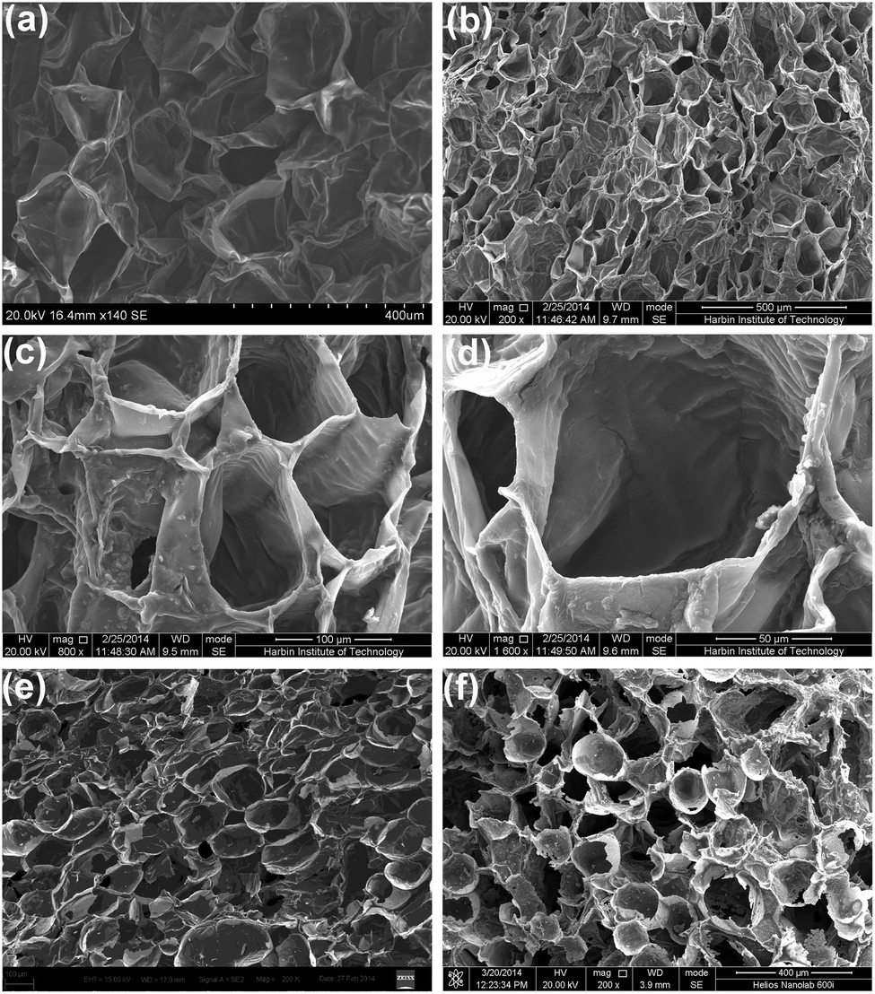 | ||
| Fig. 2 SEM images of (a) apple; (b–d) dried apple at three various magnifications; (e) carbonized apple; (f) porous SiC. | ||
Fig. 3 shows the XRD patterns of the samples. In the XRD pattern of the carbonized apple, the peak at 22.4° corresponds to the (002) plane of graphite while for the porous SiC material, a crystalline zinc-blend (cubic) form of 3C-SiC (β-SiC, JCPDS Card No. 29-1129) was found. The diffraction peaks located at 35.60°, 41.38°, 59.98°, 71.78° and 75.49° are associated with the (111), (200), (220), (311) and (222) planes of β-SiC, respectively. A small shoulder which was labelled as SF at 2θ = 34.7° is attributed to stacking faults (SFs) of the β-SiC. The SF peak is found when the mass ratio of Si:C is increased to above six. The changes in the diffractogram, which were obtained by varying the mass ratio of the precursors, reveal that the porous SiC consisted of different polytypes. The diffraction peaks at 28.5°, 47.3°, and 56.2° correspond to Si, which can be detected when the mass ratio of Si:C is below four or above six, which means that the reaction has not gone to completion. In the macroscopic view, the treated samples show elemental carbon (carbon residue) and a coating of Si on the carbon surface (excess Si powder) for the Si:C mass ratios of two or eight, respectively. Some morphological features are shown in Fig. 4.
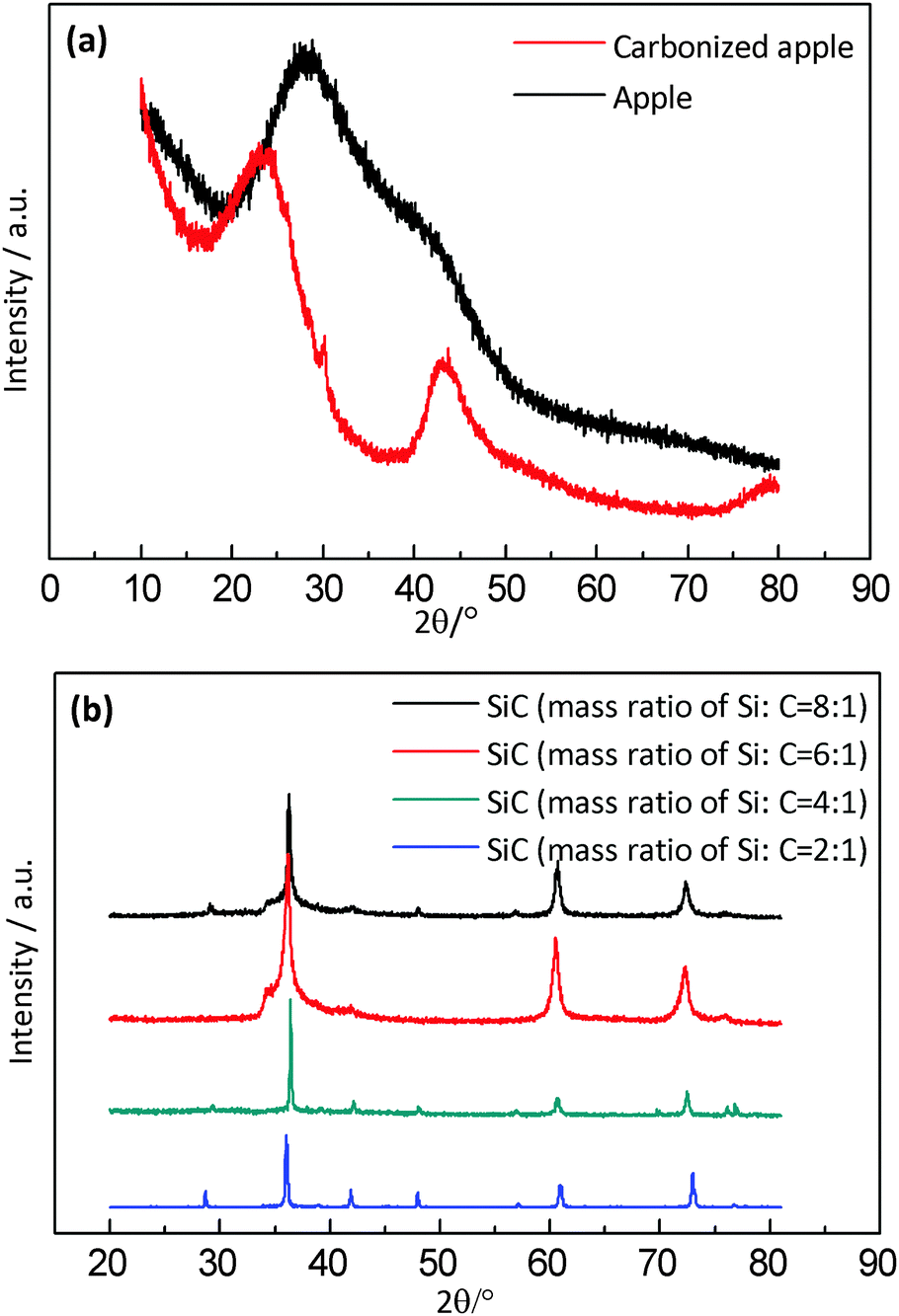 | ||
| Fig. 3 XRD patterns of (a) the apple and carbonized apple; (b) porous SiC with the Si:C mass ratio of 2:1, 4:1, 6:1, and 8:1. | ||
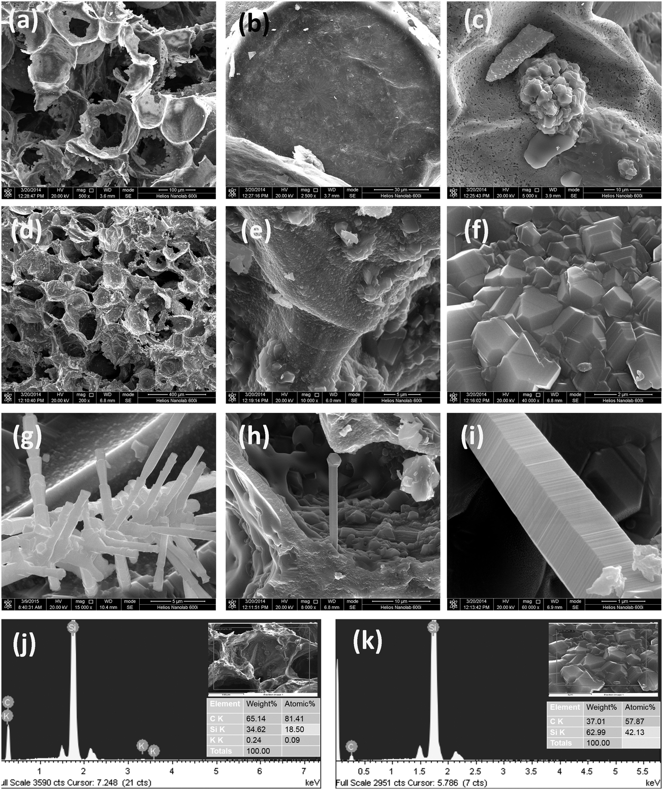 | ||
| Fig. 4 SEM images of porous SiC at different magnifications. Mass ratio of Si:C being (a–c) 4:1; (d–i) 6:1 and corresponding EDS results of the mass ratio of Si:C being (j) 4:1; (k) 6:1. | ||
The SEM images of the porous SiC (the Si:C mass ratio of 4:1) in Fig. 4a–c illustrate its characteristic porous foam structure. The porous structure has a rough surface because there are large quantities of micropores covering the surface (as shown in Fig. 4c). The EDS results in Fig. 4j show that the pore consists of Si, C and little K, meaning that the porous framework is constituted of the SiC matrix with excess carbon. Fig. 4d–f show the porous SiC (the Si:C mass ratio of 6:1) at various magnifications. Compared with the porous SiC at the starting Si:C ratio of 4:1, this porous SiC appears denser. No micro-pores could be observed, and the walls of the pores are crystalline SiC. The EDS analysis which is shown in Fig. 4k reveals that the pore consists of Si and C with the atomic ratio of approximately 1:1, since more Si participated in the reaction. From the images with higher magnifications (Fig. 4g–i), SiC fibres were found to have grown in situ on the porous framework and the diameters of the micro-fibres are in the range of 0.1–1 μm.
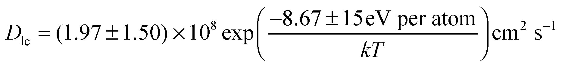
The possible mechanism for the growth of the SiC wires is explained as follows. It was mentioned earlier that the partial pressure of Si vapor was very high under the current experimental conditions. It was even higher at a higher ratio of Si:C (e.g. 6:1). FactSage37 simulation revealed that the partial pressure of carbon vapor was on the order of 1 × 10⁻¹⁴ units of atmospheric pressure under the current experimental conditions, which was 9 orders of magnitude lower than that of Si vapor. As a result, the carbon vapor contributed little to the formation of SiC. Si vapor firstly deposited on the sample surface, followed by the diffusion of carbon from inside the sample to the newly-deposited Si layer to allow their reaction leading to the formation of SiC. Si vapor concentration gradient would be developed due to its continuous consumption on the sample surface. The presence of the concentration gradient resulted in preferential deposition of Si on the tip of SiC wires, because of the presence of highest concentrations of Si vapor around the tips of SiC wires. In order to allow the continuous growth of the SiC wires, carbon needs to diffuse from the bulk of sample through the SiC wires all the way to the tips. The self-diffusion rate of C in β-SiC can be represented by eqn (2),38 where Dlc is the lattice self-diffusion coefficient of carbon in β-SiC, k is the Boltzmann constant, and T is temperature. Assuming the diffusion of carbon is the rate-limiting step in the formation of SiC wires, it was calculated that approximately 5 μm long SiC wires would form after 2 hours of reaction at 1600 °C, which is in good agreement with the observations under SEM (Fig. 4).
 | (2) |
Fig. 4i illustrates the highly populated stacking faults which are characteristic of the micro-fibres. Plenty of step-like streaked lines can be seen as strips in the domains, corresponding to the SF peak in the XRD pattern (Fig. 3b). The stacking faults could enhance the dipole polarization and magnify energy dissipation under a varying electromagnetic field.39 Therefore, such porous SiC materials are expected to exhibit good performance in the electromagnetic absorption. It is worth noticing that the two types (crystalline and fibre) of the porous SiC show different porous micro-structures, which were developed by simply changing the Si:C ratios.
EM absorption performance of the porous SiC
Generally, microwave absorption properties are determined by the complex permittivity (εr = ε′ − jε′′) and permeability (μr = μ′ − jμ′′) values. The real parts (ε′ and μ′) of the complex permittivity and permeability represent the storage capability of the electric and magnetic energies. The imaginary parts (ε′′ and μ′′) represent the loss capability of electric and magnetic energies. Fig. 5 shows the frequency dependence of the real part (ε′) and imaginary part (ε′′) of the permittivity of the samples in the range of 2–18 GHz. The real part (μ′) and imaginary part (μ′′) of permeability are 1.0 and 0.0 (not shown). It can be seen that both ε′ and ε′′ increase with the filler content (the mass ratio of Si:C being 6:1). When the loading of SiC is 60 wt%, ε′ is around 10, which is twice that when the loading is 40 wt% (ε′ ≈ 5). ε′ increases from 7.5 to 10 when the precursor Si:C mass ratio is increased from 4:1 to 6:1. Compared with the significant changes in ε′, there is little change in ε′′. β-SiC exhibits dielectric resonance features in the permittivity spectra. There is a resonance peak located at approximately 9 GHz with the loading of 60 wt% (the mass ratio of Si:C being 6:1). No obvious resonance peak can be found when the Si:C mass ratio was 4:1. We propose that the dielectric resonance of SiC is enhanced by the presence of the stacking faults. The SF phenomenon correlates with specific processing conditions (Fig. 3). The stacking faults alter the porous crystal structure of SiC, change the electric charge distribution balance and introduce orientational polarization. These enhance the permittivity.
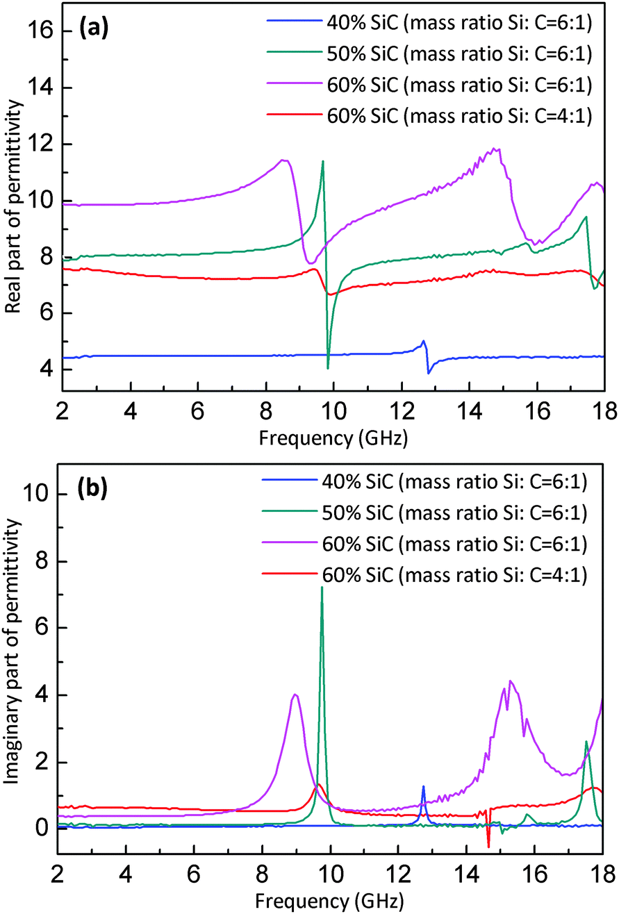 | ||
| Fig. 5 Real part (a) and imaginary part (b) of the complex permittivity spectra of the samples in the 2–18 GHz range. | ||
EM wave absorption performance is basically estimated by reflection loss (RL), which can be calculated from the complex permeability and permittivity at a given frequency (2–18 GHz) and the absorber thickness by the transmission line theory as the following equations:
 | (3) |
 | (4) |
:C mass ratio of 6:1. It can be seen that the minimum RLs are −1.1 dB at 12–14.8 GHz and −11 dB at 17.6–18 GHz with loadings of 40 wt% and 50 wt%, respectively. These composites exhibit little microwave absorption. However, a significant enhancement of the absorption ability was noted when the loading increased to 60 wt%, where the minimum RL value reaches as low as −60 dB at 17–18 GHz. This substantial enhancement of the permittivity was achieved while there was little impact on the permeability (as shown in Fig. 5). Fig. 6e demonstrates that the absorber exhibits the excellent absorption performance (RL < −10 dB) at a high frequency range from 14 to 18 GHz with a sample thickness of 4.0–5.0 mm. For comparison, the lowest reflection loss for SiC porous materials (the Si:C mass ratio being 4:1, loading 60 wt%) is −30 dB at 17.8 GHz (Fig. 6d), which demonstrates a good absorption performance. This supports the claim that the enhancement of the EM absorption (compared with that of the SiC with Si:C of 6:1, loading 60 wt%) could be attributed to the presence of stacking faults (SFs) in the β-SiC. This dependency of the EM absorption performance on the presence of stacking faults has been reported in our previous work.39Table 1 lists the EM absorption performance of some porous or SiC materials obtained from the literature. Compared to these reported materials, porous SiC shows the best performance in a high frequency range. Along with its high strength, thermal stability, oxidation and corrosion resistance, the porous SiC has the potential to become one of the best EM absorbers.
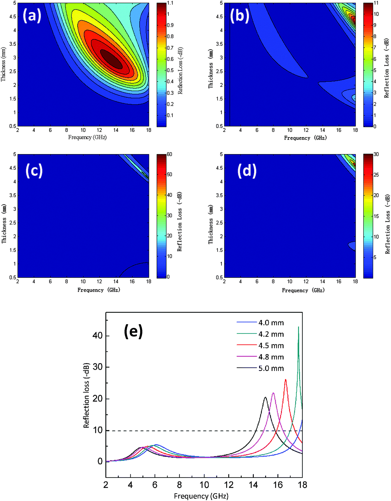 | ||
| Fig. 6 EM wave absorption characteristics of the porous SiC (Si:C mass ratio of 6:1) with loadings of (a) 40%, (b) 50% and (c) 60%; (d) porous SiC (loading 60 wt%) as a function of mass ratio of Si:C being 4:1; (e) optimal reflection loss spectra plotted against is the frequency of porous SiC with different thicknesses. | ||
EM absorption mechanism of the porous SiC
The enhanced EM absorption performance can be essentially attributed to two factors. The first factor is the presence of its unique porous structure.45–47 The porous SiC with an appropriate filler content has a well-connected architecture. The architecture was inherited from the natural honeycomb porous structure from apple, which well integrates macropores, mesopores, and micropores. The macropores guaranteed and enabled the accessibility of the mesopores and micropores. This may be critical to the remarkable increase of permittivity, which improves the impedance matching between the porous structure and the free space, which results in the high EM absorption performance. Furthermore, the porous structures inherited from nature which have a broad pore size distribution are robust and interconnected. The EM waves could easily irradiate into the porous structure. The incident waves have higher chances of being attenuated through reflection and scattering for numerous times. The absorbed electromagnetic energy must be readily converted to thermal energy. Absorption performance is enhanced significantly because the EM waves cannot escape from the porous structure.Secondly, as a typical dielectric absorber, SiC accomplishes EM absorption by intrinsic electric dipole polarization.48 The produced porous SiC with the highest stacking fault concentration exhibits the best EM absorption ability. Stacking fault enhancement of EM absorption has been previously reported by our group.39 The stacking faults in the SiC material change its crystal structure which produces a large number of vacancies, antisites and layer interruptions, and thus destroy the balance of the electric charge distribution. The SFs cause dipole fields to be introduced with dipole moments, which cause multiple dipole polarizations and orientational polarizations all of which enhance energy dissipation and, as a consequence, enhance the EM absorption.
Conclusions
Porous SiC was produced with a unique morphological structure. The fabrication took advantage of the natural micro-structure of the apple fruit. This porous SiC material showed high performance for EM absorption. The porous framework was composed of different SiC crystal structures, and the SiC polytype composition was capable of being adjusted simply by varying the mass ratio of the C and Si precursors. The stacking faults in the SiC were proposed to induce enhanced electric charge redistribution and generate extensive polarizations and energy dissipation, thus attenuating the incident EM waves. The cellular, interconnected, well-organized 3D network porous structure likely reflects and scatters the EM waves numerous times to further enhance the EM absorption performance. When the porous SiC was produced with the appropriate filler content, the reflection loss of SiC porous materials reached as low as −60 dB. The porous SiC material is promising as a cost effective, lightweight, corrosion-resistant and highly thermostable multifunctional EM absorber.Acknowledgements
The authors are deeply thankful for the financial support of the National High Technology Research and Development Program 863 (2007AA03Z337). As well, the authors would like to thank the financial support from the Daqing Petroleum Administration Bureau. The authors would also like to appreciate the scholarship of doctoral student visiting program from Harbin Institute of Technology.Notes and references
- D. R. Rolison, J. W. Long, J. C. Lytle, A. E. Fischer, C. P. Rhodes, T. M. McEvoy, M. E. Bourga and A. M. Lubers, Chem. Soc. Rev., 2009, 38, 226–252 RSC.
- R. Girgert, C. Grundker, G. Emons and V. Hanf, Bioelectromagnetics, 2008, 29, 169–176 CrossRef CAS PubMed.
- J. R. Jauchem, K. L. Ryan and M. R. Frei, Bioelectromagnetics, 2000, 21, 159–166 CrossRef CAS PubMed.
- X. Gui, J. Wei, K. Wang, A. Cao, H. Zhu, Y. Jia, Q. Shu and D. Wu, Adv. Mater., 2010, 22, 617 CrossRef CAS PubMed.
- C. Moreno-Castilla and F. J. Maldonado-Hodar, Carbon, 2005, 43, 455–465 CrossRef CAS.
- A. Richter, G. Paschew, S. Klatt, J. Lienig, K. F. Arndt and H. J. Adler, Sensors, 2008, 8, 561 CrossRef CAS.
- J. H. Zou, J. H. Liu, A. S. Karakoti, A. Kumar, D. Joung, Q. A. Li, S. I. Khondaker, S. Seal and L. Zhai, ACS Nano, 2010, 4, 7293 CrossRef CAS PubMed.
- J. Wang, C. Xiang, Q. Liu, Y. Pan and J. Guo, Adv. Funct. Mater., 2008, 18, 2995–3002 CrossRef CAS.
- J. Zhou, J. He, G. Li, T. Wang, D. Sun, X. Ding, J. Zhao and S. Wu, J. Phys. Chem. C, 2010, 114, 7611–7617 CAS.
- H. Yang, M. Cao, Y. Li, H. Shi, Z. Hou, X. Fang, H. Jin, W. Wang and J. Yuan, Adv. Opt. Mater., 2014, 2, 214–219 CrossRef.
- Z. M. Dang, T. Zhou, S. H. Yao, J. K. Yuan, J. W. Zha, H. T. Song, J. Y. Li, Q. Chen, W. T. Yang and J. Bai, Adv. Mater., 2009, 21, 2077 CrossRef CAS.
- P. C. P. Watts, W. K. Hsu, A. Barnes and B. Chambers, Adv. Mater., 2003, 15, 600–603 CrossRef CAS.
- Y. Duan, Z. Liu, H. Jing, Y. Zhang and S. Li, J. Mater. Chem., 2012, 22, 18291–18299 RSC.
- Z. Chen, C. Xu, C. Ma, W. Ren and H. M. Cheng, Adv. Mater., 2013, 25, 1296–1300 CrossRef CAS PubMed.
- L. Kong, X. W. Yin, X. Y. Yuan, Y. J. Zhang, X. M. Liu, L. F. Cheng and L. T. Zhang, Carbon, 2014, 73, 185–193 CrossRef CAS.
- M. K. Han, X. W. Yin, L. Kong, M. Li, W. Y. Duan, L. T. Zhang and L. F. Cheng, J. Mater. Chem. A, 2014, 2, 16403–16409 CAS.
- L. Kong, X. W. Yin, Y. J. Zhang, X. Y. Yuan, Q. Li, F. Ye, L. F. Cheng and L. T. Zhang, J. Phys. Chem. C, 2013, 117, 19701–19711 CAS.
- S. L. Shi and J. Liang, Nanotechnology, 2008, 19, 255707 CrossRef PubMed.
- Y. X. Gong, L. Zhen, J. T. Jiang, C. Y. Xu, W. S. Wang and W. Z. Shao, CrystEngComm, 2011, 13, 6839–6844 RSC.
- B. Wen, M. Cao, M. Lu, W. Cao, H. Shi, J. Liu, X. Wang, H. Jin, X. Fang, W. Wang and J. Yuan, Adv. Mater., 2014, 26, 3484–3489 CrossRef CAS PubMed.
- W. L. Song, M. S. Cao, M. M. Lu, J. Liu, J. Yuan and L. Z. Fan, J. Mater. Chem. C, 2013, 1, 1846–1854 RSC.
- Y. Sun, F. Xiao, X. Liu, C. Feng and C. Jin, RSC Adv., 2013, 3, 22554–22559 RSC.
- M. S. Cao, J. Yang, W. L. Song, D. Q. Zhang, B. Wen, H. B. Jin, Z. L. Hou and J. Yuan, ACS Appl. Mater. Interfaces, 2012, 4, 6948–6955 Search PubMed.
- C. Y. Liu, Y. J. Xu, L. N. Wu, Z. H. Jiang, B. Z. Shen and Z. J. Wang, J. Mater. Chem. A, 2015, 3, 10566–10572 CAS.
- G. S. Wang, Y. Wu, Y. Z. Wei, X. J. Zhang, Y. Li, L. D. Li, B. Wen, P. G. Yin, L. Guo and M. S. Cao, ChemPlusChem, 2014, 79, 375–381 CrossRef CAS.
- X. Luo, G. S. Wang, H. Y. Guo, X. J. Zhang, W. Q. Cao, Y. Z. Wei, L. Guo and M. S. Cao, ChemPlusChem, 2014, 79, 1089–1095 CrossRef CAS.
- X. J. Zhang, G. S. Wang, W. Q. Cao, Y. Z. Wei, J. F. Liang, L. Guo and M. S. Cao, ACS Appl. Mater. Interfaces, 2014, 6, 7471–7478 CAS.
- N. Leventis, A. Sadekar, N. Chandrasekaran and C. Sotiriou-Leventis, Chem. Mater., 2010, 22, 2790–2803 CrossRef CAS.
- L. S. Sigl, J. Eur. Ceram. Soc., 2003, 23, 1115–1122 CrossRef CAS.
- R. Naslain, Compos. Sci. Technol., 2004, 64, 155–170 CrossRef CAS.
- N. G. Wright and A. B. Horsfall, J. Appl. Phys., 2007, 40, 6345–6354 CAS.
- L. J. Bonderer, A. R. Studart and L. J. Gauckler, Science, 2008, 319, 1069–1073 CrossRef CAS PubMed.
- M. E. Randall, L. Rafael, R. Nuria and R. S. Andre, Science, 2012, 13, 199–204 Search PubMed.
- H. W. Liang, Q. F. Guan, L. F. Chen, Z. Zhu, W. J. Zhang and S. H. Yu, Angew. Chem., Int. Ed., 2012, 51, 5101–5105 CrossRef CAS PubMed.
- S. Deville, E. Saiz, R. K. Nalla and A. P. Tomsia, Science, 2006, 311, 515–518 CrossRef CAS PubMed.
- A. Roine, HSC Chemistry, version 6.12 for Windows, Outokumpu Research Oy, Pori, Finland, 2007 Search PubMed.
- C. W. Bale, E. Bélisle, P. Chartrand, S. A. Decterov, G. Eriksson, K. Hack, I. H. Jung, Y. B. Kang, J. Melançon, A. D. Pelton, C. Robelin and S. Petersen, CALPHAD: Comput. Coupling Phase Diagrams Thermochem., 2009, 33, 295–311 CrossRef CAS.
- M. H. Hon and R. F. Davis, J. Mater. Sci., 1979, 14, 2411–2421 CrossRef CAS.
- H. Zhang, Y. Xu, J. Zhou, J. Jiao, Y. Chen, H. Wang, C. Liu, Z. Jiang and Z. Wang, J. Mater. Chem. C, 2015, 3, 4416–4423 RSC.
- P. Xu, X. Han, B. Zhang, Y. Du and H.-L. Wang, Chem. Soc. Rev., 2014, 43, 1349–1360 RSC.
- Q. L. Liu, D. Zhang and T. X. Fan, Appl. Phys. Lett., 2008, 93, 013110 CrossRef.
- W. Xie, H. F. Cheng, Z. Y. Chu, Y. J. Zhou, H. T. Liu and Z. H. Chen, Mater. Des., 2009, 30, 1201–1204 CrossRef.
- S. C. Chiu, H. C. Yu and Y. Y. Li, J. Phys. Chem. C, 2010, 114, 1947 CAS.
- Y. K. Dou, J. B. Li, X. Y. Fang, H. B. Jin and M. S. Cao, Appl. Phys. Lett., 2014, 104, 052102 CrossRef.
- B. Zhao, G. Shao, B. B. Fan, W. Y. Zhao, Y. J. Xie and R. Zhang, J. Mater. Chem. A, 2015, 3, 10345–10352 CAS.
- B. Zhao, W. Y. Zhao, G. Shao, B. B. Fan and R. Zhang, Dalton Trans., 2015, 44, 15984–15993 RSC.
- B. Zhao, B. B. Fan, Y. W. Xu, G. Shao, X. D. Wang, W. Y. Zhao and R. Zhang, ACS Appl. Mater. Interfaces, 2015, 7, 26217–26225 CAS.
- R. B. Wu, K. Zhou, Z. H. Yang, X. K. Qian, J. Wei, L. Liu, Y. Z. Huang, L. B. Kong and L. Y. Wang, CrystEngComm, 2013, 15, 570–576 RSC.
Footnote |
| † Electronic supplementary information (ESI) available: Pictures of dried apple and carbonized apple in macroscopic size are presented. See DOI: 10.1039/c6tc01319h |
| This journal is © The Royal Society of Chemistry 2016 |