
 Open Access Article
 This Open Access Article is licensed under a
 Creative Commons Attribution 3.0 Unported Licence
Thiazole-based scaffolding for high performance solar cells†
I.
Bulut
a,
P.
Chávez
a,
A.
Mirloup
b,
Q.
Huaulmé
b,
A.
Hébraud
a,
B.
Heinrich
c,
S.
Fall
d,
S.
Méry
c,
R.
Ziessel
b,
T.
Heiser
d,
P.
Lévêque
*d and
N.
Leclerc
*a
aInstitut de Chimie et Procédés pour l’Energie, l’Environnement et la Santé (ICPEES), Département d’Ingénierie Polymère, UMR 7515 Université de Strasbourg-CNRS, 25 rue Becquerel, Strasbourg 67087, France. E-mail: leclercn@unistra.fr
bInstitut de Chimie et Procédés pour l’Energie, l’Environnement et la Santé (ICPEES), Laboratoire de Chimie Moléculaire et Spectroscopies Avancées, UMR 7515 Université de Strasbourg-CNRS, 25 rue Becquerel, Strasbourg 67087, France
cInstitut de Physique et Chimie des Matériaux de Strasbourg (IPCMS), UMR 7504 Université de Strasbourg-CNRS, 23 rue du Loess, Strasbourg 67034, France
dLaboratoire des Sciences de l'ingénieur, de l'informatique et de l'imagerie (ICube), UMR 7357 Université de Strasbourg-CNRS, 23 rue du Loess, Strasbourg 67037, France. E-mail: patrick.leveque@unistra.fr
First published on 30th March 2016
Abstract
An interesting way of decreasing both HOMO and LUMO energy levels simultaneously while keeping the band-gap constant in soluble electron-donor small molecules for photovoltaic applications is presented. This consists in the replacement of thiophene rings by thiazole units in small molecules based on the alternation of electron-rich and electron-deficient moieties. A new diketopyrrolopyrrole-based dumbbell-shaped electron-donor soluble molecule for organic photovoltaic applications has been synthesized and characterized. It includes thiazole units as linkers between the bis-lactam core and the triazatruxene moieties used as π-stacking platforms. A power conversion efficiency of 6.3% has been attained with this thiazole derivative and in particular with an increase of the open-circuit voltage of 0.15 V with respect to the thiophene-based organic semiconducting counterpart. This open-circuit voltage increase is due to the lowering of the HOMO level of the thiazole derivative while its LUMO level has also been stabilized as highlighted by the similar band-gap measured for the thiazole and thiophene derivatives.
Introduction
During the past decade, the use of organic molecules for photovoltaic applications has been spotlighted, thanks to the engineering of original chemical structures possessing suitable optoelectronic properties, reaching efficiencies of over 10%.1 Many prerequisites are required to reach the optimal conditions for efficient organic photovoltaic (OPV) cells. In particular, (i) a broad absorption range is required to maximize the harvesting of incident solar photons, (ii) the frontier energy levels have to be adjusted in such a way that a deep HOMO level (highest occupied molecular orbital) allows an increase in the open circuit voltage (Voc), while a relatively high LUMO level (lowest unoccupied molecular orbital) provides an accurate driving force for efficient exciton dissociation and charge separation and finally, (iii) strong intermolecular interactions in the solid state will be highly suitable for exciton diffusion and for charge carrier mobility affecting both the short circuit current density (Jsc) and the fill factor (FF).In light of these requirements, the engineering of electronic energy levels appears to be one of the key parameters to increase the power conversion efficiency (PCE) of OPV devices. Unfortunately, decreasing the band-gap often conflicts with the lowering of the HOMO level. Ideally, both the HOMO and LUMO energy levels should be simultaneously decreased in order to increase the Voc while keeping the band-gap constant. Such a fine energy level tuning is chemically challenging and, to the best of our knowledge, few successful approaches have been reported to date in the literature. The most common approach consists in the selective replacement of some hydrogen atoms along the conjugated backbone by fluorine atoms. Indeed, fluorine atoms act as small electron-withdrawing groups that allow a simultaneous decrease of both energy levels by about 0.15 eV. This strategy has been successfully applied to several conjugated polymers and small molecules, leading to highly efficient photovoltaic devices.2 Another method consists in the use of thioalkyl chains instead of standard alkyl side chains to bring solubility. Such a substitution has shown a weak lowering of the LUMO and a stronger lowering of the HOMO energy levels leading to higher Voc.3
In this paper, we report an alternative and efficient chemical approach to lower both frontier energy levels, based on the use of thiazole rings as weak electron-donor species. Indeed, due to its more electron-deficient nature with regard to a standard thiophene ring, we recently demonstrated that the introduction of a thiazole unit into an alternating electron-rich/electron-poor conjugated backbone appears therefore as a convenient and effective way to increase both the ionization potential and electron affinity by about 0.1 to 0.2 eV, when compared to the thiophene unit, while keeping the energy band-gap almost unchanged.4 However, a positive impact of this approach on the open-circuit voltage and power conversion efficiency has only been rarely properly demonstrated in an organic photovoltaic device5 even though the thiazole unit was previously used in semiconducting polymers.6
Therefore, we applied this chemical strategy to a small molecule in which a thiazole-substituted diketopyrrolopyrrole (TzDPP) unit is sandwiched between two triazatruxene (TAT) moieties to form a dumbbell-shaped molecular structure. We indeed recently demonstrated that such a construct, with thiophene-substituted diketopyrrolopyrrole (ThDPP), behaves as an efficient electron-donor when blended with phenyl-C71-butyric acid methyl ester (PC71BM), leading to a high PCE in solution-processed small molecule-based OPV devices.7 The DPP core is seen as a bis-lactam unit sandwiched by two aromatic substituents at the 3 and 6 positions. These two substituents behave as electron-rich π-conjugated linkers and can be easily functionalized. The modification of these linkers usually leads to a significant change in the physical and optoelectronic properties (crystal structure, thermal transitions, band gap, HOMO–LUMO levels, etc.) of DPP-based materials.8 Based on this knowledge, the synthesis and characterization of a new TAT–DPP small molecule derivative containing thiazole linking units between the DPP core and the peripheral TAT units (TAT–TzDPP in Fig. 1) is reported herein. We demonstrate, in particular, that these thiazole linkers allow a significant increase, in the Voc, allowing the PCE of bulk heterojunction devices to reach 6.3%.
 | ||
| Fig. 1 Synthetic route towards the preparation of the TAT–TzDPP dye. The left inset depicts the thiazole nomenclature. The right inset shows the reference TAT–ThDPP molecule used for reference.7 | ||
Experimental section
Synthesis
1H and 13C NMR spectra were recorded on 300 MHz and 400 MHz NMR spectrometers, with 1H and 13C chemical shifts reported in δ (ppm) relative to CDCl3 (7.26 and 77.16, respectively). MS (EI) and HRMS experiments were performed on a Bruker spectrometer within the service center at the “Institut de Chimie” of Strasbourg University.
UV-visible spectroscopy and luminescence spectroscopy
UV-visible spectra were recorded using a Shimadzu UV-3600 dual-beam grating spectrophotometer with a 1 cm quartz cell. Steady-state emission and excitation spectra were recorded at 25 °C on a HORIBA Jobin-Yvon FluoroMax 4P spectrofluorimeter. All fluorescence spectra were corrected. The fluorescence quantum yield was calculated using the following equation:where I denotes the integral of the corrected fluorescence spectrum, A is the absorbance at the excitation wavelength and n is the refractive index of the medium. Luminescence lifetimes were measured on a FL 920 Edinburgh Instruments spectrofluorimeter equipped with a R928 photomultiplier and a PicoQuant PDL 800-D pulsed diode connected to a GwInstect GFG-8015G delay generator. Emission wavelengths were selected using a monochromator. Luminescence lifetimes were measured on a spectrofluorimeter using software with Time-Correlated Single Photon Mode coupled to a stroboscopic system. The excitation source was a laser diode (λ = 310 nm). No filter was used for excitation. The instrument response function was determined by using a light-scattering solution (LUDOX).

Electrochemical measurements
Oxidation and reduction potentials were determined by cyclic voltammetry with a conventional 3-electrode system using a voltammetric analyzer equipped with a platinum micro disk (2 mm2) working electrode and a platinum wire counter electrode. Potentials were calibrated versus the saturated calomel electrode (SCE) using the ferrocene/ferricinium couple as an internal reference (+0.38 V vs. SCE) at a conventional scan rate of 200 mV s−1. Recrystallized tetrabutylammonium hexafluorophosphate (Bu4NPF6) was used as the supporting electrolyte (0.1 M) in distilled and anhydrous CH2Cl2. CH2Cl2 was distilled from P2O5 under a nitrogen atmosphere. The ferrocene/ferricinium couple was used as an internal reference.DSC measurements
DSC measurements were performed using a TA Instruments Q1000 instrument, operated at a scanning rate of 5 °C min−1 upon heating and upon cooling.Results and discussion
The starting building block 16c (Fig. 1) was prepared and purified according to the literature procedure. The synthesis of 2-bromo-TAT (2) is detailed in the Experimental section. The nature of this 2-bromo-TAT (2) isomer has been unambiguously assigned by reference to the 3-bromo-TAT isomer synthesized by an independent protocol (see the ESI† supported by Fig. S1 to S10).To synthesize the TAT–TzDPP dye (3), an original and selective direct arylation cross-coupling was preferred to the standard Suzuki cross-coupling previously used for the thiophene derivative.7 This cleaner and atom-economical cross-coupling reaction has been carried out between compounds 1 and 2 in the presence of the palladium-Herrmann catalyst, phosphine ligand [P(p-MeOC6H4)3], Cs2CO3 as a base and pivalic acid as an additive, leading to the target TAT–TzDPP compound (3) with 54% yield after purification. This catalyst system makes this cross-coupling reaction highly regioselective taking place selectively in the C5-position of the thiazole unit.4b,10
The NMR spectral analysis of the final TAT–TzDPP molecule shows only one singlet peak at 8.30 ppm, which is assigned to the thiazole proton in the C4-position, in agreement with previous studies (Fig. S11).4b,11 The only by-product of this condensation reaction that has been isolated is the mono-coupling compound. This direct arylation cross-coupling appears even more efficient if we consider that the dibromination of the TzDPP derivative is often described with reaction yields of only 20–30% after purification.5,6b All compounds were characterized by standard NMR and mass spectrometry.
The electronic spectra (absorption and emission) of the new DPP dye are shown in Fig. 2 and Fig. S13 (ESI†). The absorption spectrum of TAT–TzDPP in solution shows an intense peak at around 657 nm (ε = 85![[thin space (1/6-em)]](https://www.rsc.org/images/entities/char_2009.gif) 000 M−1 cm−1) corresponding to the lowest energy π–π* transitions (S0 → S1) of the DPP chromophore.13,14 The marked shoulder at higher energy of this intense absorption is typical of the vibronic sequence (Δν = 1230 cm−1) of a bis-lactam framework.15 Another weaker transition at ca. 500 nm is likely due to an internal charge transfer (ICT) transition in keeping with previous observations.16,17 The strong transition recorded at about 320 nm (ε = 130000 to 180000 M−1 cm−1) is assigned to π–π* transitions of the fused tris-carbazole platform.18 The dye fluorescence observed in THF shows a maximum emission at about 757 nm. The emission profile (Fig. S13, ESI†) does not mirror the absorption one, indicating a polarized excited state typical of a charge transfer state. A large Stokes shift of 2000–3900 cm−1 and a short lifetime (about 2 ns) also confirm the emission from a charge transfer state.13,14
000 M−1 cm−1) corresponding to the lowest energy π–π* transitions (S0 → S1) of the DPP chromophore.13,14 The marked shoulder at higher energy of this intense absorption is typical of the vibronic sequence (Δν = 1230 cm−1) of a bis-lactam framework.15 Another weaker transition at ca. 500 nm is likely due to an internal charge transfer (ICT) transition in keeping with previous observations.16,17 The strong transition recorded at about 320 nm (ε = 130000 to 180000 M−1 cm−1) is assigned to π–π* transitions of the fused tris-carbazole platform.18 The dye fluorescence observed in THF shows a maximum emission at about 757 nm. The emission profile (Fig. S13, ESI†) does not mirror the absorption one, indicating a polarized excited state typical of a charge transfer state. A large Stokes shift of 2000–3900 cm−1 and a short lifetime (about 2 ns) also confirm the emission from a charge transfer state.13,14
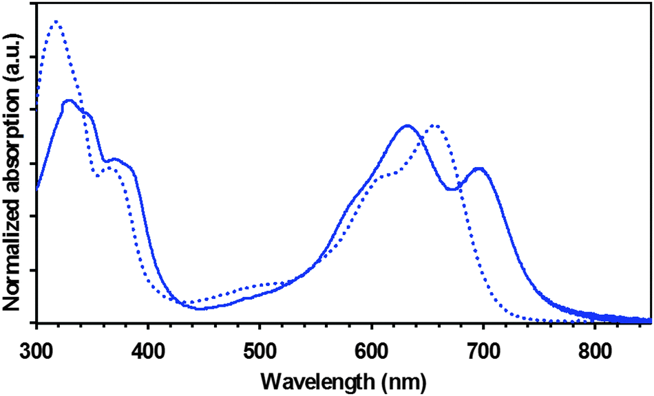 | ||
| Fig. 2 Normalized absorption in solution (dashed lines) and in thin-film (full lines) of TAT–TzDPP. | ||
The quantum yield is rather weak (3%). The emission band is slightly broader and the excited state lifetime drops down to 0.55 ns and the emission properties show a high solvent polarity sensitivity (Fig. S14, ESI†). Interestingly, by decreasing the dipole moment of the solvent (from THF to toluene) the intensity of the emission band of TAT–TzDPP increases as well as the corresponding excited state lifetime (QY from 3% to 46%, lifetime from 0.55 to 3.06 ns). The sensitivity of the emission to the polarity of the solvent is in favor of an ICT-like emission.13,14
The thin film absorption spectrum (full line in Fig. 2) shows a significant bathochromic shift in comparison to its solution counterpart due to stronger intermolecular interactions in the solid state. The amplitude shift is roughly 40 nm from the band edge. From the solid-state absorption onset, an optical gap of 1.65 eV has been calculated for TAT–TzDPP.
The cyclic voltammetry in dilute solution allows for the determination of the frontier molecular orbital energies (HOMO/LUMO levels) after calibration with ferrocene used as an internal reference. The voltammogram (Fig. 3) displays several well-defined and reversible waves, which can be assigned, by comparison with reference to isolated synthons, to the constitutive molecular modules of the compound. As previously observed, the TAT fragment is not electroactive in the anodic window, whereas the DPP moieties display two reversible reduction waves (Fig. 3).13,14
 | ||
| Fig. 3 Cyclic voltammogram in dichloromethane for TAT–TzDPP using TBAPF6 as the supporting electrolyte. | ||
The first reduction wave is located at −0.93 V. Note that most of the redox processes appear to be reversible (ipa/ipc ≈ 1) and exhibit the characteristic shape (ΔEp = 60–70 mV) of a Nernstian, one-electron process. The second reduction wave is located at −1.49 V. Each reduction is monoelectronic and according to previous reports, the reduction processes are assigned to the formation of the radical anion and dianion of the substituted bis-lactam central core.13,16 The positive potential region is much richer and shows several oxidation waves.
The TAT substrate exhibits three reversible monoelectronic oxidations in the +0.50 to +1.40 V potential range (Fig. 3), in agreement with the literature data,7,16 while the TzDPP core exhibits one reversible oxidation wave, located at +0.67 V. The electrochemical gap, deduced from the HOMO/LUMO level positions, is 1.60 eV and this value is in line with the optical gap reported above (Table 1). Electrochemical data are summarized in Table S1 in the ESI.†
| Solution | Thin film | ||||||||
|---|---|---|---|---|---|---|---|---|---|
| λ abs (nm) | ε (M−1 cm−1) | λ em (nm) | Φ@λex, (nm) | τ (ns) | K p (108 s−1) | k nr (108 s−1) | Δ ss (cm−1) | λ abs (nm) | ΔEg (eV) |
a
Φ was calculated from 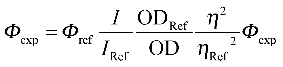 with rhodamine 6G (Φref = 0.78)12 in air equilibrated water and tetramethoxydiisoindomethene-difluoroborate (Φref = 0.51) as references.
b
k
r was calculated from with rhodamine 6G (Φref = 0.78)12 in air equilibrated water and tetramethoxydiisoindomethene-difluoroborate (Φref = 0.51) as references.
b
k
r was calculated from  .
c
k
nr was calculated from .
c
k
nr was calculated from  . .
|
|||||||||
| 657 | 85000 |
757 | 0.03@600 | 0.55 | 0.55 | 17.6 | 2000 | 695 | 1.65 |
At this stage it is worth pointing out the large difference in frontier orbital energies observed between the TzDPP-based compound and the previously reported thiophene derivative (see the structure in the inset of Fig. 1), despite their similar absorption properties (see Fig. S15, ESI,† for solid state absorption comparison).7 Indeed, the oxidation and reduction potentials measured for TAT–TzDPP are consistently up-shifted in comparison with TAT–ThDPP [Eoxy = +0.47 V and Ered = −1.24 V].7 As a result, both HOMO and LUMO energy levels of the thiazole derivative are significantly down-shifted by around 0.20 eV with regard to the thiophene derivative. By considering that the open-circuit voltage (Voc) of an organic photovoltaic device is strongly dependent on the offset between the LUMO level of the electron acceptor and the HOMO level of the electron donor,19 we may expect a higher Voc when the TAT–TzDPP dye is used as the electron donor, keeping almost constant the photon harvesting properties for both TAT–TzDPP and TAT–ThDPP dyes. We note that the offset between the LUMO of the electron-donor molecule and the LUMO of the electron acceptor PC71BM (measured under the same conditions at −4.20 eV)7 is equal to 350 meV for TAT–TzDPP. This offset should be sufficient for efficient charge separation.20
Thermal properties have been characterized by differential scanning calorimetry (DSC) and thermal gravimetric analysis (TGA). Both materials exhibit a remarkable thermal stability with degradation temperatures above 300 °C (Fig. S16, ESI†). Unlike a recent series of amorphous TAT-based systems bearing ramified chains,21 the face-to-face close packing of TAT segments is here authorized by the less sterically demanding linear chains. It then allows the self-organization of the dye in various structures delaying the phase transition toward the isotropic liquid to 240–270 °C (see DSC in Fig. S17, ESI†). Despite the similar shape of conjugated moieties and the identical peripheral chains, the self-organization behavior of TAT–TzDPP turns out to be different from the previously reported TAT–ThDPP.7 The latter dye is a semi-crystalline solid as deduced from optical polarizing microscopy (POM) and confirmed by powder small-angle X-ray scattering (SAXS) analyses (see Fig. S18, ESI†). In contrast, TAT–TzDPP is mesomorphous and gives rise to birefringent (but not-characteristic) POM textures that progressively become fluid upon heating. A columnar mesophase-like piling is confirmed by SAXS, as a semi-diffuse peak hTAT at 3.8 Å from distances between piled TAT segments (correlation length ξ ≈ 5 nm upon cooling from 110 °C) overlaps the broad wide-angle scattering hch,Tz at around 4.5 Å from liquid-like lateral distances between chains and thiazole linkers (see Fig. S18 and S19, ESI†). In the small-angle range a somewhat broadened reflection DTAT at 17.6 Å arises from the arrangement of TAT piles separated from each other by the undifferentiated continuum formed by disordered chains and linkers. The structure however deviates from a genuine columnar mesophase as the linking units introduce a three-dimensional geometrical character and a structural disorder, which explains the reduced correlation length (ξ ≈ 13 nm) and the unresolved higher order reflections. In this view, the mesomorphism of TAT–TzDPP appears to be the consequence of the absence of self-organization of the thiazole segments that prevents the crystallization of the whole molecule.
Charge transport properties have been determined in organic field effect transistor (OFET) devices with a bottom contact-bottom gate configuration. Details of the OFET device fabrication can be found in the ESI.† The output and transfer FET characteristics for as-cast TAT–TzDPP can be seen in Fig. 4. The hole mobility was extracted in the saturation regime using the standard formalism. This value is reasonably high, in the order of 3.8 × 10⁻³ cm2 V−1 s−1 for TAT–TzDPP, and should be compared with the previously reported mobility of the thiophene analogue (TAT–ThDPP, 4.4 × 10⁻⁴ cm2 V−1 s−1).7
 | ||
| Fig. 4 Output characteristics (left) and transfer characteristics (right) of an as-cast TAT–TzDPP OFET. For the output characteristics, the gate voltage (Vg) is increased from 0 to −70 V with a −10 V step. For the transfer characteristics in the saturation regime, the drain–source voltage (Vds) is set at −100 V and Vg is varied from 0 to −100 V. | ||
We note a substantially higher in-plane hole mobility for the mesomorphic TAT–TzDPP compared to the crystalline compound. Hole-only devices with an ITO/PEDOT:PSS/small molecule/MoO3/Ag structure were elaborated to estimate the out-of-plane hole mobility in the space charge limited current (SCLC) regime. Details of the SCLC device fabrication as well as the (I–V) characteristics for two different TAT–TzDPP thicknesses can be found in the ESI.† The out-of-plane hole mobility was estimated to be as high as 3.7 × 10⁻² and 1.5 × 10⁻³ cm2 V−1 s−1 for TAT–ThDPP and TAT–TzDPP, respectively. For TAT–TzDPP, the out-of-plane hole mobility is lower than the in-plane hole mobility as expected from the dependence of the mobility as a function of the charge carrier concentration.22 On the other hand, the out-of-plane hole mobility is almost two orders of magnitude higher than the in-plane hole mobility for TAT–ThDPP, suggesting a high charge-transport anisotropy for this crystalline compound.22
Organic photovoltaic (OPV) devices were elaborated using both a standard and an inverted device architecture. For the standard architecture (anode on the transparent side of the device) the following layer sequence was used: ITO/PEDOT:PSS/active layer/Ca/Al. For the inverted architecture (cathode on the transparent side of the device), the recently reported 80% ethoxylated polyethylenimine (PEIE) was used as the interface layer.23 The use of a thin layer of this polymer having pendant alkylamine groups is known to reduce the work function of ITO and can be processed in air from non-toxic alcoholic solutions. A reflective MoO3/Ag electrode has been used to collect holes on the top surface of the device. In all the cases, the active layers were made up of blends of TAT-based molecular compounds and PC71BM and were deposited by spin-coating from chloroform solutions. Thermal annealing at 120 °C for 10 minutes was performed before Ca/Al or MoO3/Ag evaporation. Each OPV device consists of four diodes, each of them having an active area of 12 mm.2 Each condition has been tested at least twice. Other details of OPV device fabrication can be found in the ESI.†
Electrical parameters of OPV devices are summarized in Table 2. Note that the standard deviations as well as the averaged PCE reported values were calculated from 6 to 10 diodes on different substrates elaborated under the same conditions. The fact that the best results were obtained on a standard architecture for TAT–ThDPP and on an inverted one for TAT–TzDPP is not clear at this stage and is still under investigation.
| Compound | Device structurea | Dye:PC71BM ratio |
V oc (V) | J sc (mA cm−2) | FF (%) | PCEb (%) | Thickness (nm) |
|---|---|---|---|---|---|---|---|
| a S for standard and I for inverted. b The standard deviation for each parameter is provided in parentheses. | |||||||
| TAT—TzDPP | S | 1:0.75 |
0.698 (0.002) | 7.2 (0.6) | 49.0 (3) | 2.50 (0.3) | 145 |
| I | 0.798 (0.004) | 13.21 (0.08) | 58.8 (1.2) | 6.10 (0.1) | |||
| TAT—ThDPP | S | 1:0.75 |
0.630 (0.02) | 14.4 (0.2) | 57.0 (1.5) | 5.21 (0.05) | 115 |
| I | 0.610 (0.01) | 10.4 (0.4) | 46.9 (1.6) | 2.99 (0.18) | |||
The main trends that can be drawn from the photovoltaic properties meet our predictions. First of all, the lowest open circuit voltage (Voc) values are found for the TAT–ThDPP compound which is in agreement with its higher lying HOMO level.19 Second, the short-circuit current density (Jsc), which depends in part on the absorption range of the compounds, is found to be similar in both thiophene and thiazole derivatives. As expected from the almost identical molecular shapes, the dye:PC71BM ratios needed to optimize the device performance are of 1:0.75 for both derivatives. This observation suggests that the different structural features between both derivatives do not affect their intermixing process with PC71BM and thus the percolation pathways for electron transport.24
The best photovoltaic performances were measured on TAT–TzDPP devices that combine a high Voc value (in the 0.7–0.8 V range) because of their low lying HOMO level, with a high Jsc value (more than 13 mA cm−2) due to their moderate optical band-gap (1.65 eV) and a high FF value of around 59%.
Consequently, when we compare the best TAT–ThDPP photovoltaic results (in the standard structure) with the best TAT–TzDPP photovoltaic results (in the inverted structure), the thiazole-compound devices exhibit a comparable Jsc (13.2 mA cm−2 and 14.4 mA cm−2 for TAT–ThDPP) value but a substantially higher Voc value (0.80 V and 0.63 V for TAT–ThDPP). Consequently, with a FF in the same range for both compounds (slightly below 60%), the average power conversion efficiency is increased from 5.2% to 6.1% when Tz is used in the electron-donor small molecule.
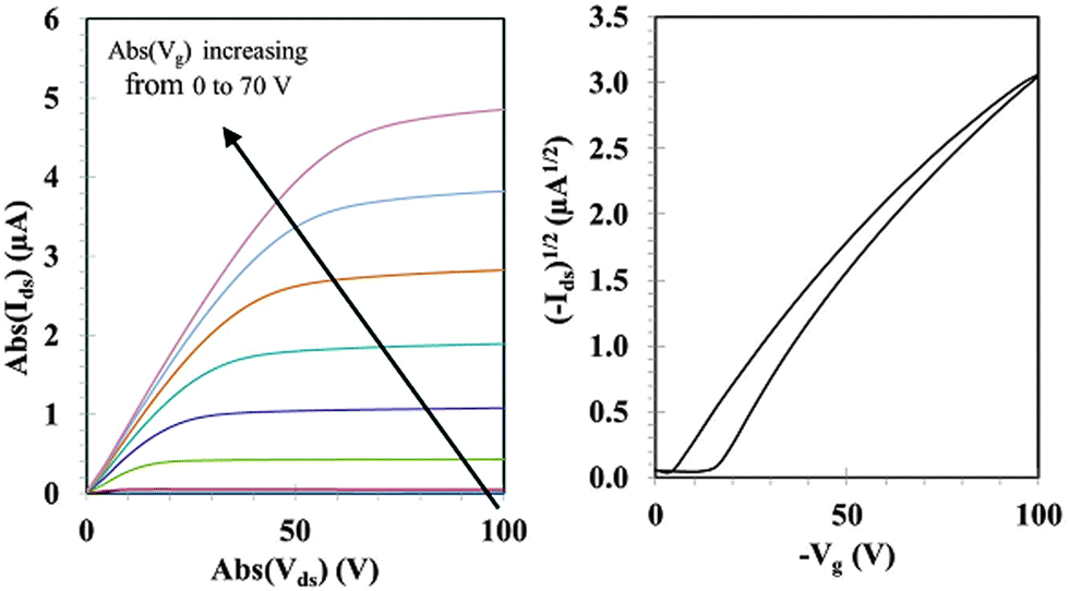
Though the size of the statistical samples is limited (10 diodes for each best condition), the conclusion drawn here is unambiguous as the relative Voc increase (more than 25%) when using Tz instead of Th is significantly higher than the standard deviation of the measured Voc values (Table 2). A maximum PCE of 6.3% (Voc = 0.79 V; Jsc = 13.3 mA cm2; FF = 60%) has been reached with TAT–TzDPP against 5.3% for TAT–ThDPP. The (J–V) curves for the best photovoltaic devices using TAT–ThDPP and TAT–TzDPP are shown in Fig. 5. It can be noticed that in both cases, the best results were obtained without the help of additives.
 | ||
| Fig. 5 (J–V) curves obtained in the dark (black symbols) and under standard AM1.5G (100 mW cm−2) illumination conditions (colored symbols). The squares correspond to the TAT–ThDPP compound (standard architecture) and the circles to the TAT–TzDPP compound (inverted architecture). | ||
Investigations of the optimized thin-film morphology of the new compound TAT–TzDPP in blend with PC71BM have been carried out by means of GIWAXS measurements. In the case of TAT–TzDPP, GIWAXS patterns (see Fig. 6 and S20) show, for a ratio of 1:0.75 with PC71BM, a clear phase segregation of both components with the coexistence of mesomorphous TAT–TzDPP domains and amorphous PC71BM domains. It can be noticed that the preferential π-stacking direction is parallel to the meridian, which is favorable for a π-stacking charge transport perpendicular to the substrate plane.
 | ||
| Fig. 6 GIWAXS pattern of TAT–TzDPP:PC71BM (ratio of 1:0.75) recorded after annealing at 120 °C for 10 min. | ||
The investigation of the active layer surface morphology of a TAT–TzDPP:PC71BM blend (an optimal photovoltaic ratio of 1:0.75) by dynamic amplitude modulation atomic force microscopy (tapping mode) under ambient conditions showed a smooth surface (peak/valley roughness below 7 nm), with a slight domain size increase after thermal annealing (around 40 nm on average, see Fig. S21, ESI†). The latter could lead to a more efficient bicontinuous interpenetrating network in thermally annealed active layers with regard to as-deposited thin films.
The external quantum efficiency (EQE) of one TAT–TzDPP device is shown in Fig. S24 (ESI†). The difference between the Jsc calculated from the EQE spectrum and the Jsc measured under standard AM1.5G (100 mW cm−2) on the same device is below the measurement error margin (less than 5%). As the EQE measurements are performed at significantly lower light intensity, this result indicates that the charge carrier recombination rate does not depend significantly on the light intensity in this device. Moreover, the EQE spectrum exhibits values above 60% over a broad spectral range (580–700 nm), which is comparable with the state-of-the-art small molecule based solar cells.25
Conclusions
In summary, we have designed and synthesized a soluble small molecule engineered from a combination of diketopyrrolopyrrole (DPP) and triazatruxene (TAT) moieties for use in organic photovoltaic solar cells. We have demonstrated that the thiazole unit could be used efficiently as an alternative to the thiophene unit in an electron-donor molecule. In particular, we have shown that replacing a thienyl ring by a thiazole is an effective approach to stabilizing both HOMO and LUMO levels while keeping the initial photon harvesting properties of the organic semiconducting materials unchanged. A maximum PCE of 6.3% has thus been reached using a thiazole-based molecule and in particular with an increase of the Voc of 0.15 V with respect to the thiophene counterparts. Thiazole was until now mainly identified as an interesting electron deficient moiety, leading to efficient electron acceptor organic semiconducting materials.26 The present result highlights that the thiazole ring also constitutes a good candidate for building efficient electron donor organic semiconducting (macro)molecules for OPV. Finally, the high potential of this emerging DPP/aryl/TAT family of molecules for solution-processed BHJ solar cells was confirmed and further structural modifications in combination with other highly light-harvesting units are currently ongoing in our research laboratories.Acknowledgements
Ibrahim Bulut and Patricia Chávez contributed equally to this work. This work was supported by the Interreg IV-A program under Rhin-Solar project (nr C25) and the French National Research Agency (ANR ORION project ANR-13-PRGE-0001). Elsa Cece, Dr Thomas Bura and Nicolas Zimmermann are acknowledged for the preparation of some of these compounds and devices. We thank the Pohang Accelerator Laboratory (PAL) for giving us the opportunity to perform the GIWAXS measurements, MEST and POSTECH for supporting these experiments, Drs Tae Joo Shin and Hyungju Ahn for adjustments and help, and other colleagues from the 9A USAXS beamline for assistance. Dr P. Montgomery is acknowledged for his careful reading of the manuscript and his suggestions for the English spelling. This research was supported by Leading Foreign Research Institute Recruitment Program through the National Research Foundation of Korea (NRF) funded by the Ministry of Science, ICT & Future Planning (NRF-2010-00453).References
- (a) A. Mishra and P. Bäuerle, Angew. Chem., Int. Ed., 2012, 51, 2020 CrossRef CAS PubMed; (b) P. M. Beaujuge and J. M. J Fréchet, J. Am. Chem. Soc., 2011, 133, 20009 CrossRef CAS PubMed; (c) B. Kan, M. Li, Q. Zhang, F. Liu, X. Wan, Y. Wang, W. Ni, G. Long, X. Yang, H. Feng, Y. Zuo, M. Zhang, F. Huang, Y. Cao, T. P. Russell and Y. Chen, J. Am. Chem. Soc., 2015, 137, 3886 CrossRef CAS PubMed.
- (a) D. Dang, W. Chen, R. Yang, W. Zhu, W. Mammo and E. Wang, Chem. Commun., 2013, 49, 9335 RSC; (b) J. Wolf, F. Cruciani, A. El Labban and P. M. Beaujuge, Chem. Mater., 2015, 27, 4184 CrossRef CAS; (c) P. Yang, M. Yuan, D. F. Zeigler, S. E. Watkins, J. A. Lee and C. K. Luscombe, J. Mater. Chem. C, 2014, 2, 3278 RSC; (d) N. Leclerc, P. Chávez, O. A. Ibraikulov, T. Heiser and P. Lévêque, Polymers, 2016, 8, 11 CrossRef.
- (a) K. Feng, X. Xu, Z. Li, Y. Li, K. Li and T. Yu, Chem. Commun., 2015, 51, 6290 RSC; (b) C. Cui, W.-Y. Wong and Y. Li, Energy Environ. Sci., 2014, 7, 2276 RSC; (c) C. Cui, X. Guo, J. Min, B. Guo, X. Cheng, M. Zhang, C. J. Brabec and Y. Li, Adv. Mater., 2015, 27, 7469 CrossRef CAS PubMed; (d) C. Cui, Z. He, Y. Wu, X. Cheng, H. Wu, Y. Li, Y. Cao and W.-Y. Wong, Energy Environ. Sci., 2016, 9, 885 RSC.
- (a) E. Zaborova, P. Chávez, R. Bechara, P. Lévêque, T. Heiser, S. Méry and N. Leclerc, Chem. Commun., 2013, 49, 9938 RSC; (b) P. Chávez, C. Ngov, P. De Frémont, P. Lévêque and N. Leclerc, J. Org. Chem., 2014, 79, 10179 CrossRef PubMed.
- J.-L. Wang, Z. Wu, J.-S. Miao, K.-K. Liu, Z.-F. Chang, R.-B. Zhang, H.-B. Wu and Y. Cao, Chem. Mater., 2015, 27, 4338 CrossRef CAS.
- (a) H. Bronstein, E. Collado-Fregoso, A. Hadipour, Y. Soon, Z. Huang, S. D. Dimitrov, R. Shahid Ashraf, B. P. Rand, S. E. Watkins, P. S. Tuladhar, I. Meager, J. R. Durrant and I. McCulloch, Adv. Funct. Mater., 2013, 23, 5647 CrossRef CAS; (b) W. Li, K. H. Hendriks, A. Furlan, M. M. Wienk and R. A. J. Janssen, J. Am. Chem. Soc., 2015, 137, 2231 CrossRef CAS PubMed; (c) B. Carsten, J. M. Szarko, L. Lu, H. J. Son, F. He, Y. Y. Botros, L. X. Chen and L. Yu, Macromolecules, 2012, 45, 6390 CrossRef CAS.
- T. Bura, N. Leclerc, R. Bechara, P. Lévêque, T. Heiser and R. Ziessel, Adv. Energy Mater., 2013, 3, 1118 CrossRef CAS.
- J. Dhar, N. Venkatramaiah, A. Anitha and S. Patil, J. Mater. Chem. C, 2014, 2, 3457 RSC.
- W. A. Herrmann, C. Brossmer, K. Öfele, C.-P. Reisinger, T. Priermeier, M. Beller and H. Fischer, Angew. Chem., Int. Ed. Engl., 1995, 34, 1844 CrossRef CAS.
- S. Tani, T. N. Uehara, J. Yamaguchi and K. Itami, Chem. Sci., 2014, 5, 123 RSC.
- A. K. Palai, S. P. Mishra, A. Kumar, R. Srivastava, M. N. Kamalasanan and M. Patri, Eur. Polym. J., 2010, 46, 1940 CrossRef CAS.
- J. Olmsted, J. Phys. Chem., 1979, 83, 2581 CrossRef CAS.
- (a) A. Iqbal and L. Cassar, US Pat., 4, 415, 685, Nov 15, 1983 Search PubMed; (b) J. Pfenninger, A. Iqbal and A. C. Rochat, Eur. Pat., 184-981, June 18, 1986 Search PubMed; (c) M. Jost, A. Iqbal and A. C. Rochat, Eur. Pat., 224-445, June 3, 1987 Search PubMed.
- D. Hablot, P. Retailleau and R. Ziessel, Chem. – Eur. J., 2010, 6, 13346 CrossRef PubMed.
- A. Iqbal, M. Jost, R. Kirchmayr, J. Pfenninger, A. C. Rochat and O. Wallquist, Bull. Soc. Chim. Belg., 1988, 97, 615 CrossRef CAS.
- L. Dou, W.-H. Chang, J. Gao, C.-C. Chen, J. You and Y. Yang, Adv. Mater., 2013, 25, 825 CrossRef CAS PubMed.
- A. Sutter, P. Retailleau, W.-C. Huang, H.-W. Lin and R. Ziessel, New J. Chem., 2014, 38, 1701 RSC.
- (a) T. Bura, N. Leclerc, S. Fall, P. Lévêque, T. Heiser and R. Ziessel, Org. Lett., 2011, 13, 6030 CrossRef CAS PubMed; (b) C. Ruiz, J. T. López Navarrete, M. C. Ruiz Delgado and B. Gómez-Lor, Org. Lett., 2015, 17, 2258 CrossRef CAS PubMed.
- M. C. Scharber, D. Mühlbacher, M. Koppe, P. Denk, C. Waldauf, A. J. Heeger and C. J. Brabec, Adv. Mater., 2006, 18, 789 CrossRef CAS.
- J. L. Brédas, D. Beljonne, V. Coropceanu and J. Cornil, Chem. Rev., 2004, 104, 4971 CrossRef PubMed.
- I. Bulut, P. Lévêque, B. Heinrich, T. Heiser, R. Bechara, N. Zimmermann, S. Méry, R. Ziessel and N. Leclerc, J. Mater. Chem. A, 2015, 3, 6620 CAS.
- S. Fall, L. Biniek, Y. Odarchenko, D. V. Anokhin, G. de Tournadre, P. Lévêque, N. Leclerc, D. A. Ivanov, O. Simonetti, L. Giraudet and T. Heiser, J. Mater. Chem. C, 2016, 4, 286 RSC.
- Y. Zhou, C. Fuentes-Hernandez, J. Shim, J. Meyer, A. J. Giordano, H. Li, P. Winget, T. Papadopoulos, H. Cheun, J. Kim, M. Fenoll, A. Dindar, W. Haske, E. Najafabadi, T. M. Khan, H. Sojoudi, S. Barlow, S. Graham, J.-L. Brédas, S. R. Marder, A. Kahn and B. Kippelen, Science, 2012, 336, 327 CrossRef CAS PubMed.
- S. Fall, L. Biniek, N. Leclerc, P. Lévêque and T. Heiser, Appl. Phys. Lett., 2012, 101, 123301 CrossRef.
- B. Kam, M. Li, Q. Zhang, F. Liu, X. Wan, Y. Wang, W. Ni, G. Long, X. Yang, H. Feng, Y. Zuo, M. Zhang, F. Huang, Y. Cao, T. P. Russel and Y. Chen, J. Am. Chem. Soc., 2015, 137, 3886 CrossRef PubMed.
- Y. Lin, H. Fan, Y. Li and X. Zhan, Adv. Mater., 2012, 24, 3087 CrossRef CAS PubMed.
Footnote |
| † Electronic supplementary information (ESI) available: Experimental techniques, synthesis and characterization of the dyes (Fig. S1–S12), absorption and emission spectra (Fig. S13–S15), redox potentials (Table S1), thermogravimetric and DSC analyses (Fig. S16 and S17), SAXS and GIWAXS spectra (Fig. S18–S20), AFM images (Fig. S21) and the EQE spectrum (Fig. S22). See DOI: 10.1039/c6tc00531d |
| This journal is © The Royal Society of Chemistry 2016 |