 Open Access Article
Creative Commons Attribution 3.0 Unported Licence
Facile preparation of copper nitride powders and nanostructured films†
Robert
Szczęsny
*ab,
Edward
Szłyk
b,
Marek A.
Wiśniewski
bc,
Tuan K. A.
Hoang
a and
Duncan H.
Gregory
*a
aWestCHEM, School of Chemistry, University of Glasgow, Glasgow, G12 8QQ, UK. E-mail: Duncan.Gregory@Glasgow.ac.uk
bNicolaus Copernicus University in Toruń, Faculty of Chemistry, 87-100 Toruń, Poland. E-mail: Robert.Szczesny@umk.pl
cINVEST-TECH R&D Center, 32-34 Plaska St., 87-100 Toruń, Poland
First published on 26th April 2016
Abstract
The simple fluorinated precursor, copper(II) trifluoroacetate, Cu(CF3COO)2 can be effectively utilised in the synthesis of copper(I) nitride, Cu3N, powders and films by combinations of wet processing and gas–solid (ammonolysis) techniques. The resulting materials were characterized by powder X-ray diffraction (PXD), scanning electron microscopy (SEM) with energy dispersive X-ray spectroscopy (EDX), atomic force microscopy (AFM), diffuse reflectance UV-visible spectroscopy (DRUV-Vis), Raman spectroscopy, infrared spectroscopy (IR), thermogravimetric-differential thermal analysis-mass spectrometry (TG-DTA-MS) and nitrogen adsorption (BET) analysis. Moreover, variable temperature IR (VT-IR) studies of the solid phase were performed in situ during ammonolysis. Single-phase Cu3N powders composed of sub-micron scale platelets can be produced over relatively short reaction times. Materials prepared in this way are stoichiometric narrow band gap semiconductors. The same trifluoroacetate precursor was used to prepare nanostructured nitride films by spin coating. The surface microstructure was investigated and evaluated relative to films deposited by dip coating and nebulisation using the soluble carboxylate precursor.
Introduction
Copper nitride is an indirect band-gap semiconductor with a high electrical resistivity and a low reflectivity which can find potential application in optical storage,1–4 as a component of spintronic systems5,6 or as a potential electrode material for rechargeable Li-ion batteries.7 Coatings of Cu3N can also be used to generate microscopic metal lines and dots since copper nitride is thermally unstable and can easily decompose into nitrogen and pure metallic copper.8 The deposited copper metal has a significantly higher reflectivity and conductivity than the nitride and this decomposition process can be easily induced by electron beam or laser irradiation. In contrast to tellurium-based light recording media, Cu3N is non-toxic and stable at ambient conditions.9 Consequently, the nitride can be used for the fabrication of either metallic Cu or composite Cu/Cu3N microscopic structures.10 Structures of this type can be employed as the basis of advanced magnetic devices such as spin valves6 or used to probe complex nanoscale phenomena such as the spin excitations of Mn antiferromagnetic chains.5 Cu3N has a cubic anti-ReO3 type structure (space group Pm![[3 with combining macron]](https://www.rsc.org/images/entities/char_0033_0304.gif) m) where nitrogen atoms are located at the corners of the primitive unit cell and copper atoms occupy the 3d edge sites. Given the open nature of the structure, in some circumstances it is possible to insert metal atoms at the interstitial body centre (1/2, 1/2, 1/2) position.11,12 The addition of other transition metals (TMs) modifies the electronic properties of Cu3N and in the case of 3d metals offers a promising route to produce magnetic semiconductors.3,13 Films of copper nitride have been primarily fabricated by physical methods such as reactive RF magnetron sputtering14–16 or pulsed laser deposition (PLD).17,18 However, chemical synthesis routes to powders of Cu3N predate these studies by several decades. Juza and Rabenau19 first synthesized Cu3N in 1956 by heating a CuF2 precursor under a flow of gaseous ammonia. The same precursor was used by Gregory et al. to prepare single phase material for powder neutron diffraction studies.20 Further, in 1990 Zachwieja and Jacobs demonstrated that polycrystalline Cu3N could be prepared without the need for ammonia via the direct thermal decomposition reaction of [Cu(NH3)x]NO3.21 It is also possible to synthesise the nitride in a solvothermal reaction by heating copper azide in organic solvents at moderate temperature,22 by using Cu(NO3)2 and primary amines as capping agents23,24 or by reacting ammonia with copper(II) acetate monohydrate dispersed in long chain alcohols.25,26 Moreover, it is even possible to utilise copper(I) oxide as a precursor using either ammonia gas or urea as a nitrogen source.27
m) where nitrogen atoms are located at the corners of the primitive unit cell and copper atoms occupy the 3d edge sites. Given the open nature of the structure, in some circumstances it is possible to insert metal atoms at the interstitial body centre (1/2, 1/2, 1/2) position.11,12 The addition of other transition metals (TMs) modifies the electronic properties of Cu3N and in the case of 3d metals offers a promising route to produce magnetic semiconductors.3,13 Films of copper nitride have been primarily fabricated by physical methods such as reactive RF magnetron sputtering14–16 or pulsed laser deposition (PLD).17,18 However, chemical synthesis routes to powders of Cu3N predate these studies by several decades. Juza and Rabenau19 first synthesized Cu3N in 1956 by heating a CuF2 precursor under a flow of gaseous ammonia. The same precursor was used by Gregory et al. to prepare single phase material for powder neutron diffraction studies.20 Further, in 1990 Zachwieja and Jacobs demonstrated that polycrystalline Cu3N could be prepared without the need for ammonia via the direct thermal decomposition reaction of [Cu(NH3)x]NO3.21 It is also possible to synthesise the nitride in a solvothermal reaction by heating copper azide in organic solvents at moderate temperature,22 by using Cu(NO3)2 and primary amines as capping agents23,24 or by reacting ammonia with copper(II) acetate monohydrate dispersed in long chain alcohols.25,26 Moreover, it is even possible to utilise copper(I) oxide as a precursor using either ammonia gas or urea as a nitrogen source.27
In this work we describe the preparation of copper nitride by ammonolysis of copper trifluoroacetate, Cu(CF3COO)2 for the first time. The advantages of using this fluorinated ligand are two-fold: first, previous studies have indicated that the volatility of Ag(C2F5COO) and Ag(C3F7COO) under nitrogen is such that they can decompose at low temperatures via well-defined pathways to yield high purity products.28 Therefore, this type of compound has found application in chemical vapour deposition (CVD) processes.29,30 Given the standard enthalpy of formation for Cu3N (ΔHf = 74.5 kJ mol−1),31 it is vital to perform ammonolysis under a strict temperature regime. In this context, the thermolysis of copper(II) trifluoroacetate should occur below the decomposition temperature of copper nitride.32 Second, use of soluble salts offers the opportunity for facile, inexpensive solution-based methods to deposit precursor films for subsequent solid–vapour reactions. Hence, in this article, we report how copper(II) trifluoroacetate can be exploited to produce both powder and thin film samples of copper nitride. In each case, the precursor can be employed under relatively mild conditions to yield sub-micron sized crystalline products.
Experimental
Copper(II) trifluoroacetate was prepared as reported previously33 by reaction of basic copper(II) carbonate (analytical grade, POCh, Poland) with trifluoroacetic acid (99%, Aldrich) in a water–ethanol solution. The elemental analysis and IR spectra confirmed the composition of the carboxylate.Ammonolysis experiments were performed in a horizontal tube furnace. In each reaction, up to 0.4 g of precursor powder was placed in an alumina boat (60 × 50 × 50 mm) and transferred to the furnace. In all cases the maximum temperatures were reached in ∼45 min and NH3 gas (BOC, 99.98%) was used as the nitriding agent. The detailed experimental conditions are listed in Table 1. Any adsorbed ammonia was removed by treating post-ammonolysed samples under vacuum (10−3 torr) at room temperature for 30 min.
All films were deposited onto 10 mm × 10 mm × 1 mm silicon substrates by spin coating. A saturated solution of copper(II) carboxylate in THF![[thin space (1/6-em)]](https://www.rsc.org/images/entities/char_2009.gif) :
:![[thin space (1/6-em)]](https://www.rsc.org/images/entities/char_2009.gif) methanol (ACS, POCh) (5
methanol (ACS, POCh) (5![[thin space (1/6-em)]](https://www.rsc.org/images/entities/char_2009.gif) :
:![[thin space (1/6-em)]](https://www.rsc.org/images/entities/char_2009.gif) 1) was spun onto the substrate at 2000–5000 rpm for 30–120 s and each plate was subsequently dried at a rotation speed of 5000 rpm for 20 s. The coatings were then dried under vacuum for 1 h. Two alternative deposition methods were also assessed. First, the same solution as above was nebulised using a concentric glass nebulizer and the resulting mist was swept onto the silicon plate using compressed nitrogen. The carboxylate solution was deposited onto the plates in ∼30 s and the nozzle–substrate distance was 15 cm. Second, comparative dip-coating was performed using a solution of Cu(CF3COO)2, which was prepared by dissolution of 0.1 g of the copper salt in 30 ml of ethylene glycol. The silica plates used as substrates for deposition were immersed and withdrawn vertically in the solution and dried in air. The process was repeated sequentially 10 times for each sample. Ammonolysis of the films was performed at 310 °C/300 min or 300 °C/240 min. The film formation parameters are listed in Table 2.
1) was spun onto the substrate at 2000–5000 rpm for 30–120 s and each plate was subsequently dried at a rotation speed of 5000 rpm for 20 s. The coatings were then dried under vacuum for 1 h. Two alternative deposition methods were also assessed. First, the same solution as above was nebulised using a concentric glass nebulizer and the resulting mist was swept onto the silicon plate using compressed nitrogen. The carboxylate solution was deposited onto the plates in ∼30 s and the nozzle–substrate distance was 15 cm. Second, comparative dip-coating was performed using a solution of Cu(CF3COO)2, which was prepared by dissolution of 0.1 g of the copper salt in 30 ml of ethylene glycol. The silica plates used as substrates for deposition were immersed and withdrawn vertically in the solution and dried in air. The process was repeated sequentially 10 times for each sample. Ammonolysis of the films was performed at 310 °C/300 min or 300 °C/240 min. The film formation parameters are listed in Table 2.
| Sample | Deposition conditions time/s; speed/rpm | Sample | Deposition conditions time/s; speed/rpm |
|---|---|---|---|
| A | 10; 500 | J | 30; 3000 |
| B | 120; 2000 | K | 60; 4000 |
| C | 30; 2000 | L | 120; 4000 |
| D | 60; 3000 | M | 180; 5000 |
| E | 30; 4000 | N | 180; 3000 |
| F | 60; 5000 | O | 10; 4000 |
| G | 300; 5000 | P | Nebulisation |
| H | 10; 5000 | R | Dip-coating |
| I | 30; 1000 | ||
Bulk powder products were characterized by PXD using Philips XPERT Pro θ–2θ and Bruker D8 diffractometers with CuKα1 and CuKα radiation, respectively. Phase identification was performed by search-match procedures with access to the ICDD powder diffraction file (PDF) and by comparison to patterns generated from ICSD data using PowderCell v.2.3.34 Structure refinement was performed using the GSAS-II program package,35 (data were collected from 10 ≤ 2θ/° ≤ 110, with a step size of 0.0084° 2θ and at a scanning rate of 0.02° min−1). Scanning electron microscopy (SEM) studies were performed with three instruments: (1) a LEO 1430 VP microscope (Cambridge Ltd) equipped with a Quantax 200 spectrometer (XFlash 4010 detector, Bruker AXS) for energy dispersive X-ray (EDX) spectroscopy (HV mode, SE, EHT = 10–20 kV, beam current 100 μA); (2) a Philips XL 30 environmental (E)SEM equipped with an Oxford Instruments INCA Energy 250 EDX system (EHT = 20 kV, spot size 5) and (3) a Quanta 3D FEG (EHT = 30 kV) instrument. Samples of powders and films deposited onto Si were placed onto carbon tabs attached to aluminium SEM stubs. All samples were analysed in the microscope without coating treatment. Atomic Force Microscopy (AFM) analysis of films was performed using a Veeco microscope (Digital Instruments) with an NSG-11 probe (scan size 2–10 μm; scan rate 1 Hz, tapping mode).
The IR spectra (including diffuse reflectance spectra; DRIFTS) of precursors, powder products and films were obtained using a Perkin-Elmer 2000 FT IR spectrometer. Raman spectra of copper nitride were collected at room temperature using a Horiba LabRAM HR confocal microscope system with a 532 nm green laser. Diffuse reflectance (DR) UV-Vis spectra (using a Varian Cary 500 Spectrophotometer) were used to measure the optical band-gap energy of powder samples. Absorption was measured over wavelengths from 300–2000 nm.
Additionally, in situ FTIR studies (using a Mattson-Genesis II spectrometer) were performed of the heterogeneous reactions of Cu(CF3COO)2 films loaded on mica and exposed to an NH3 atmosphere. The composition of the gas phase in contact with the sample was also monitored by FTIR. Single beam spectra with only gases in the beam and spectra with both the sample and gases in the beam were taken. The ratio of these spectra allows the gaseous absorption to be subtracted, giving the absorbance due to modification of the Cu(CF3COO)2 film. Additionally, the attenuated total reflectance (ATR) technique (using a SPECAC Silver Gate with Ge crystal) was employed to characterise the final product of the ammonolysis.
The thermal behaviour of copper nitride powders was investigated by thermogravimetric-differential thermal analysis (TG-DTA) under a flowing argon atmosphere using a Netzsch STA 409PC TG-DTA instrument coupled to evolved gas analysis by MS (Hiden HPR20 mass spectrometer). Samples were heated from 30–500 °C at a heating rate of 5 °C min−1 and maintained at this temperature for 2 h. The surface areas of the synthesized materials were determined by applying the BET method to nitrogen adsorption–desorption data, which were collected at liquid nitrogen temperature using a Micromeritics Gemini instrument.
Results and discussion
Cu3N powder characterisation
![[double bond, length as m-dash]](https://www.rsc.org/images/entities/char_e001.gif) N) or ν(C
N) or ν(C![[double bond, length as m-dash]](https://www.rsc.org/images/entities/char_e001.gif) C)), 1441 cm−1, 1115/1048 cm−1 (ν(C
C)), 1441 cm−1, 1115/1048 cm−1 (ν(C![[double bond, length as m-dash]](https://www.rsc.org/images/entities/char_e001.gif) C), ν(C
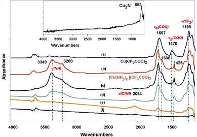
C), ν(C![[double bond, length as m-dash]](https://www.rsc.org/images/entities/char_e001.gif) N) or C–H deformation vibration bonding types) and 2926 (ν(C–H)) (Fig. S1, ESI†).37 The presence of these bands would strongly indicate that the reaction is not complete. In the case of experiment 2 (300 °C, 45 min) a peak at 651 cm−1 was registered, although this broad band cannot be unambiguously associated with the presence of nitride. Other IR bands for 2 appear at 1146, 1560, 2130 and 3328 cm−1 and can be related to the vibration of single and multiple C–N bonds and N–H bonds (Fig. S2, ESI†). By following the ammonolysis reaction in situ, the FTIR results reveal several steps over the course of the reaction (Fig. 1). The spectrum of dehydrated Cu(CF3COO)2 (Fig. 1a) consists mainly of bands that can be attributed to carboxylates (1667 and 1470 cm−1) and CF3 groups (1198 and 1151 cm−1). When the sample is exposed to an ammonia atmosphere, ammonium salts begin to form readily at room temperature (Fig. 1b) and the characteristic bands of the precursor decrease while new signals of [Cu(NH3)n](CF3COO)2 appear at 1630 and 1425 cm−1. A rise in temperature to 150 °C (Fig. 1c) results in no changes to the spectrum, but by 175 °C the intensities of all the established IR signals decrease and a new band appears at 2050 cm−1.
N) or C–H deformation vibration bonding types) and 2926 (ν(C–H)) (Fig. S1, ESI†).37 The presence of these bands would strongly indicate that the reaction is not complete. In the case of experiment 2 (300 °C, 45 min) a peak at 651 cm−1 was registered, although this broad band cannot be unambiguously associated with the presence of nitride. Other IR bands for 2 appear at 1146, 1560, 2130 and 3328 cm−1 and can be related to the vibration of single and multiple C–N bonds and N–H bonds (Fig. S2, ESI†). By following the ammonolysis reaction in situ, the FTIR results reveal several steps over the course of the reaction (Fig. 1). The spectrum of dehydrated Cu(CF3COO)2 (Fig. 1a) consists mainly of bands that can be attributed to carboxylates (1667 and 1470 cm−1) and CF3 groups (1198 and 1151 cm−1). When the sample is exposed to an ammonia atmosphere, ammonium salts begin to form readily at room temperature (Fig. 1b) and the characteristic bands of the precursor decrease while new signals of [Cu(NH3)n](CF3COO)2 appear at 1630 and 1425 cm−1. A rise in temperature to 150 °C (Fig. 1c) results in no changes to the spectrum, but by 175 °C the intensities of all the established IR signals decrease and a new band appears at 2050 cm−1.
According to the literature, the new band could be assigned to a CNN stretch.37 By 310 °C, the band at 2050 cm−1 is no longer present and the only feature in the spectrum is the band attributable to Cu3N (650 cm−1, Fig. 1 inset). Near-identical IR spectra were obtained for samples 3–6.
Significantly, the powder X-ray diffraction patterns of 1 and 2 contained no Bragg peaks and hence did not reveal any crystalline phases. In contrast, powder patterns obtained for samples 3–6 clearly demonstrate the presence of Cu3N (Fig. 2 and Fig. S3, ESI†). In the case of thin films deposited on mica, copper nitride reflections dominate with some traces of metallic copper also observed (Fig. S4 and S5, ESI†). The Raman spectra of 3–6 reveal peaks at 275 and 610 cm−1. According to the literature, the two bands at 220 and 634 cm−1 are indicative of copper nitride,38 corroborating the results above from FTIR spectroscopy. Thermogravimetric-differential thermal analysis (TG-DTA) performed for 3 under flowing argon demonstrates that the sample is thermally stable up to 349 °C. Above this temperature the product starts to decompose to Cu and N2 (as indicated by the MS spectrum of the evolved gas). This process corresponds to a mass loss of 7.0% (cf. the theoretical nitrogen content of 6.8 wt%).
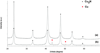 | ||
| Fig. 2 X-ray diffraction patterns of (a) 3 (prepared at 300 °C, 240 min) and (b) 6 (350 °C, 240 min). | ||
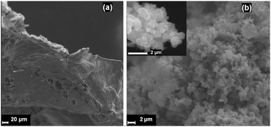
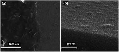
SEM/EDX analyses were used to investigate the morphology and elemental composition of materials produced under different conditions. Samples 1 and 2 took the form of a dense mass or cake of agglomerated powders (Fig. 3a). EDX spectra yielded elemental compositions with Cu![[thin space (1/6-em)]](https://www.rsc.org/images/entities/char_2009.gif) :
:![[thin space (1/6-em)]](https://www.rsc.org/images/entities/char_2009.gif) N
N![[thin space (1/6-em)]](https://www.rsc.org/images/entities/char_2009.gif) :
:![[thin space (1/6-em)]](https://www.rsc.org/images/entities/char_2009.gif) F ratios of 1
F ratios of 1![[thin space (1/6-em)]](https://www.rsc.org/images/entities/char_2009.gif) :
:![[thin space (1/6-em)]](https://www.rsc.org/images/entities/char_2009.gif) 0.4
0.4![[thin space (1/6-em)]](https://www.rsc.org/images/entities/char_2009.gif) :
:![[thin space (1/6-em)]](https://www.rsc.org/images/entities/char_2009.gif) 0.6 (RSD [%] Cu
0.6 (RSD [%] Cu![[thin space (1/6-em)]](https://www.rsc.org/images/entities/char_2009.gif) :
:![[thin space (1/6-em)]](https://www.rsc.org/images/entities/char_2009.gif) N
N![[thin space (1/6-em)]](https://www.rsc.org/images/entities/char_2009.gif) :
:![[thin space (1/6-em)]](https://www.rsc.org/images/entities/char_2009.gif) F = 3
F = 3![[thin space (1/6-em)]](https://www.rsc.org/images/entities/char_2009.gif) :
:![[thin space (1/6-em)]](https://www.rsc.org/images/entities/char_2009.gif) 19
19![[thin space (1/6-em)]](https://www.rsc.org/images/entities/char_2009.gif) :
:![[thin space (1/6-em)]](https://www.rsc.org/images/entities/char_2009.gif) 15) and 1
15) and 1![[thin space (1/6-em)]](https://www.rsc.org/images/entities/char_2009.gif) :
:![[thin space (1/6-em)]](https://www.rsc.org/images/entities/char_2009.gif) 1.8
1.8![[thin space (1/6-em)]](https://www.rsc.org/images/entities/char_2009.gif) :
:![[thin space (1/6-em)]](https://www.rsc.org/images/entities/char_2009.gif) 0.1 (RSD [%] Cu
0.1 (RSD [%] Cu![[thin space (1/6-em)]](https://www.rsc.org/images/entities/char_2009.gif) :
:![[thin space (1/6-em)]](https://www.rsc.org/images/entities/char_2009.gif) N
N![[thin space (1/6-em)]](https://www.rsc.org/images/entities/char_2009.gif) :
:![[thin space (1/6-em)]](https://www.rsc.org/images/entities/char_2009.gif) F = 3
F = 3![[thin space (1/6-em)]](https://www.rsc.org/images/entities/char_2009.gif) :
:![[thin space (1/6-em)]](https://www.rsc.org/images/entities/char_2009.gif) 16
16![[thin space (1/6-em)]](https://www.rsc.org/images/entities/char_2009.gif) :
:![[thin space (1/6-em)]](https://www.rsc.org/images/entities/char_2009.gif) 33) for 1 and 2 respectively. The elemental ratios can be rationalized in terms of the progress of the ammonolysis reaction. In the initial stages of the reaction, NH3 partially reacts with the precursor to induce formation of carbon–nitrogen bonds. Although 1 and 2 are X-ray amorphous, these bonds are visible as bands in the IR spectra. Given the relatively high nitrogen content of sample 2, we can assume that the temperature has a major impact on the conversion process (regardless of the reduced reaction time compared to 1). Volatile species are likely formed during ammonolysis at higher reaction temperatures, finally resulting in the reduction to elemental copper (samples 5 and 6) (as indicated by PXD in Fig. 2). Complete conversion to Cu3N without further reduction was observed for samples 3 and 4 and EDX analysis of 3 yielded a Cu
33) for 1 and 2 respectively. The elemental ratios can be rationalized in terms of the progress of the ammonolysis reaction. In the initial stages of the reaction, NH3 partially reacts with the precursor to induce formation of carbon–nitrogen bonds. Although 1 and 2 are X-ray amorphous, these bonds are visible as bands in the IR spectra. Given the relatively high nitrogen content of sample 2, we can assume that the temperature has a major impact on the conversion process (regardless of the reduced reaction time compared to 1). Volatile species are likely formed during ammonolysis at higher reaction temperatures, finally resulting in the reduction to elemental copper (samples 5 and 6) (as indicated by PXD in Fig. 2). Complete conversion to Cu3N without further reduction was observed for samples 3 and 4 and EDX analysis of 3 yielded a Cu![[thin space (1/6-em)]](https://www.rsc.org/images/entities/char_2009.gif) :
:![[thin space (1/6-em)]](https://www.rsc.org/images/entities/char_2009.gif) N ratio of ca. 2.8
N ratio of ca. 2.8![[thin space (1/6-em)]](https://www.rsc.org/images/entities/char_2009.gif) :
:![[thin space (1/6-em)]](https://www.rsc.org/images/entities/char_2009.gif) 1 (RSD [%] Cu
1 (RSD [%] Cu![[thin space (1/6-em)]](https://www.rsc.org/images/entities/char_2009.gif) :
:![[thin space (1/6-em)]](https://www.rsc.org/images/entities/char_2009.gif) N = 3
N = 3![[thin space (1/6-em)]](https://www.rsc.org/images/entities/char_2009.gif) :
:![[thin space (1/6-em)]](https://www.rsc.org/images/entities/char_2009.gif) 7). Moreover, SEM micrographs demonstrated that 3 and 4 form as a porous matrix of sub-micron sized particles. Each faceted particle is of the order of 200–500 nm in diameter (Fig. 3b).
7). Moreover, SEM micrographs demonstrated that 3 and 4 form as a porous matrix of sub-micron sized particles. Each faceted particle is of the order of 200–500 nm in diameter (Fig. 3b).
Nitrogen adsorption–desorption isotherms of sample 3 could be classified as type II, which represent nonporous solids (Fig. S3, ESI†).53 The adsorption isotherm is essentially linear in the range of P/P0 = 0–0.7 and condensation adsorption emerges in the region from P/P0 ∼ 0.8 to 1.0. The specific surface area of the sample is relatively low at 3.34 m2 g−1. The total pore volume is ∼0.038692 cm3 g−1 and reinforces the premise that most of the surface area of the sample is external and that the majority of structural nitrogen species are located in the bulk (as lattice N atoms) rather than on the (internal or external) surface of the material.54
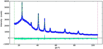
![[3 with combining macron]](https://www.rsc.org/images/entities/char_0033_0304.gif) m). The refinement conditions and final atomic parameters are listed in Table 3 and an observed, calculated and difference profile plot for the refinement is presented in Fig. 4. The background, zeropoint and scale factor were varied in the initial cycles of the refinement. A log interpolation function with 20 coefficients was applied for background refinement. Cell parameters, profile parameters and atomic parameters were then refined in order. In the final stages, all parameters were refined simultaneously until the residuals were minimized and the refinement reached convergence. Atomic parameters and interatomic distances can be found in the ESI† (Table S1).
m). The refinement conditions and final atomic parameters are listed in Table 3 and an observed, calculated and difference profile plot for the refinement is presented in Fig. 4. The background, zeropoint and scale factor were varied in the initial cycles of the refinement. A log interpolation function with 20 coefficients was applied for background refinement. Cell parameters, profile parameters and atomic parameters were then refined in order. In the final stages, all parameters were refined simultaneously until the residuals were minimized and the refinement reached convergence. Atomic parameters and interatomic distances can be found in the ESI† (Table S1).
| Radiation | X-ray |
| Instrument | D8 Bruker Advance diffractometer |
| Temperature/K | 293 |
| Formula, Z | Cu3N, 1 |
| Crystal system, space group | Cubic, Pm![[3 with combining macron]](https://www.rsc.org/images/entities/char_0033_0304.gif) m m |
| Lattice parameter, a/Å | 3.7543(3) |
| Cell volume, V/Å3 | 52.917(4) |
| No of observations, parameters | 10![[thin space (1/6-em)]](https://www.rsc.org/images/entities/char_2009.gif) 529, 28 529, 28 |
| R wp/% | 3.12 |
| χ 2 | 1.29 |
Thin film characterisation
Spin-coating, dip coating and nebulisation experiments with copper trifluoroacetate were used to compare the differences in morphology, size, and size distribution of the microcrystals for each of the different deposition methods. A precursor – THF![[thin space (1/6-em)]](https://www.rsc.org/images/entities/char_2009.gif) :
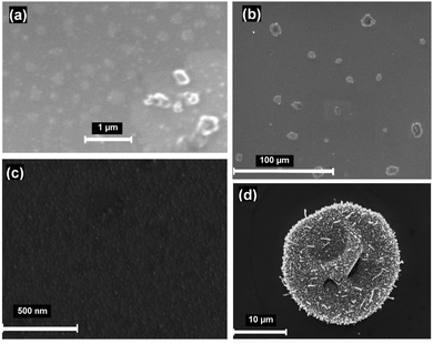
:![[thin space (1/6-em)]](https://www.rsc.org/images/entities/char_2009.gif) MeOH solution was used for both spin-coating and nebulisation experiments. The plates were examined by both optical microscopy and SEM following deposition. In most cases it was observed that materials were deposited as separated grains or/and islands of microcrystals and hence the coating layers were discontinuous (Fig. 5a, b and d). The largest islands are tens of microns in size (Fig. 5b and c). After the ammoniation process almost spherical particles of the order of 10 μm in diameter are clearly visible and each particle is composed of clusters of irregular nanocrystals and wires of sub-micron dimensions (Fig. 5d). However, for some samples uniform and continuous nanometric layers were observed to form between the “islands” (Fig. 5c). In these cases, the island-like structures (Fig. 6a) could be a result of unequal subsequent material deposition into the pinholes of the films. The homogeneous layer consists of grains of several tens of nanometres in size, existing partly in the form of denser agglomerations (Fig. 6b).
MeOH solution was used for both spin-coating and nebulisation experiments. The plates were examined by both optical microscopy and SEM following deposition. In most cases it was observed that materials were deposited as separated grains or/and islands of microcrystals and hence the coating layers were discontinuous (Fig. 5a, b and d). The largest islands are tens of microns in size (Fig. 5b and c). After the ammoniation process almost spherical particles of the order of 10 μm in diameter are clearly visible and each particle is composed of clusters of irregular nanocrystals and wires of sub-micron dimensions (Fig. 5d). However, for some samples uniform and continuous nanometric layers were observed to form between the “islands” (Fig. 5c). In these cases, the island-like structures (Fig. 6a) could be a result of unequal subsequent material deposition into the pinholes of the films. The homogeneous layer consists of grains of several tens of nanometres in size, existing partly in the form of denser agglomerations (Fig. 6b).
As might be expected, variations in the spin coating parameters have a substantial impact on the deposited surface. Irregular randomly distributed aggregates, of a few millimetres in size, are visible at speeds of 500 and 1000 rpm. At higher speeds the distribution of the material is much more regular. EDX results confirm that samples E, G and L deposited and heated under ammonia at 300 and 310 °C contain copper. Nitrogen was present substantially in areas of the film where the coverage was continuous and deposition thickness greatest. These results might suggest that a proportion of deposited copper nitride had decomposed under these conditions and improvements to the compositional homogeneity might be achieved by ammonolysis of the films at lower temperatures (compared to bulk powders). However, we note also that in the case of very thin well-dispersed coatings, the EDX detection limit does not permit unequivocal quantitative identification of light elements such as nitrogen. Indeed, the characteristic sharp band at ca. 660 cm−1 in DRIFT spectra measured from these films strongly corroborates the presence of copper nitride (ESI,† Fig. S6).
The surface morphology and the distribution of the grains after ammonolysis were also investigated by AFM. Fig. 7a shows the AFM image of a spin-coated film of B deposited from the trifluoroacetate solution and annealed under flowing NH3 at 300 °C for 4 h. There are two types of distinct particles; small particles are under 50 nm across with a height of ca. 10 nm while larger particles form with diverse diameters varying from 150–300 nm and heights between 70–100 nm. Both types of particle are evenly distributed across the surface of the plate.
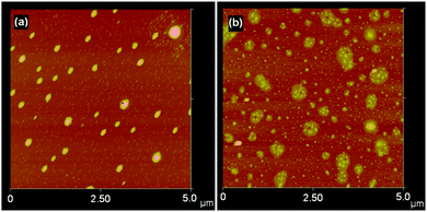 | ||
| Fig. 7 AFM images of material deposited on to Si substrates and ammonolysed: (a) from spin coating (sample B); (b) via nebulisation (sample P). | ||
The topography of the surface fabricated via nebulisation (sample P, Fig. 7b) is different from the spin-coated samples. By comparison to the spin coated sample, the coverage of the substrate was more complete but islands rather than a continuous film remained. Individual grains exhibited comparable sizes (50–100 nm across) to those observed in spin coated samples. Additionally, we examined the preparation of Cu3N films by dipping silicon plate substrates in ethylene glycol solutions followed by ammonolysis reactions at 300 °C (Fig. 8). As for spin coated and nebulized samples, the films have non-uniform distributions and only partially cover the silicon plates. This results in areas across the substrate with different concentrations of the deposited material. The most common observed topography is shown in Fig. 8a. In this case, EDX analysis produced no convincing evidence for nitrogen in these films. Similar elemental analysis results were recorded for areas containing more densely packed material (Fig. 8b). By contrast, the presence of nitrogen was confirmed in the areas of films that were the most uniform in coverage (consisting of fine grains of average size about 300 nm; Fig. 8c).
 | ||
| Fig. 8 Representative SEM images of the dip-coated sample (R) after heating under ammonia, showing: (a) the predominant form of the deposited layer and (b), (c) specific areas of the film. | ||
Deposition and ammonolysis experiments suggest therefore that future studies should focus on optimizing processing methods to improve the quality and homogeneity of the films. Moreover, results suggest that the ammonolysis of nanostructured films deposited onto silicon may require milder conditions (e.g. lower temperature) than the equivalent process for bulk powders.
To the best of our knowledge, there are no previously published studies concerning fabrication of Cu3N films by chemical deposition methods. In fact, so-called “wet chemistry methods” have been utilised relatively rarely for preparation of any nitride films. Among previous examples are the formation of silicon nitride films using a sol–gel process combined with dip-coating57 and the preparation of smooth, crack-free boron nitride films by spin coating.58 In this latter case, the nitride film was obtained by spinning a polyborazine precursor onto a substrate, followed by pyrolysis.
Application of solution methods to prepare metal nitride thin films are sparse.59 Noteworthy, is a report by Luo et al. describing the polymer-assisted deposition (PAD) of a series of metal-nitride layers such as TiN, AlN, GaN and NbN.60,61 In the PAD process, the polymer not only controls the viscosity of the metal–polymer solution but can also bind the metal ions often facilitating a homogenous distribution of the precursor. From our own experimental data and from those in the literature, it can be presumed that the selection of solvent (solutions) plays an important role in the deposition and can have a positive impact on enhanced film uniformity. Pinholes such as those observed in our experiments usually indicate a local de-wetting and defects such as pinholes and “islands” were also observed for films produced by the PAD process.62 Hence, although both results herein and by PAD suggest that near-uniform layers can be deposited, optimisation of these processes seems to be the most important task towards achieving defect-free films. The previous studies and the work described herein should act as an incentive to researchers to continue to expend effort in developing relatively inexpensive and easy chemical methods for deposition of nanostructured nitride films.
Conclusions
Sub-micron powders of Cu3N can be produced by ammonolysis reactions using Cu(CF3COO)2 as precursor over a temperature range of 300–310 °C. Annealing in an ammonia atmosphere at 350 °C or higher leads to Cu3N decomposition accompanied by reduction of copper(II) to metallic copper. The value of the band gap for powders produced from copper(II) trifluoroacetate was 1.48 eV and is comparable with literature data for the nitride. BET measurements classify the powders as nonporous solids. The use of carboxylate solution-based precursors provides a facile route to nitride thin film deposition and the quality and structure of these films can be controlled via appropriate choice of precursor and processing conditions.Acknowledgements
The study was supported by a research fellowship for R. S. within the “Enhancing the Educational Potential of Nicolaus Copernicus University in the Disciplines of Mathematical and Natural Sciences” project (project no. POKL.04.01.01-00-081/10). D. H. G thanks EPSRC for funding for T. K. A. H. under grant EP/I022570/1.Notes and references
- Z. Ji, Y. Zhang, Y. Yuan and C. Wang, Mater. Lett., 2006, 60, 3758 CrossRef CAS.
- R. Cremer, M. Witthaut, D. Neuschütz, C. Trappe, M. Laurenzis, O. Winkler and H. Kurz, Microchim. Acta, 2000, 133, 299 CrossRef CAS.
- X. Y. Cui, A. Soon, A. E. Phillips, R. K. Zheng, Z. W. Liu, B. Delley, S. P. Ringer and C. Stampil, J. Magn. Magn. Mater., 2012, 324, 3138 CrossRef CAS.
- G. H. Yue, P. X. Yan, J. Z. Liu, M. X. Wang, M. Li and X. M. Yuan, J. Appl. Phys., 2005, 98, 103506 CrossRef.
- C. F. Hirjibehedin, C. P. Lutz and A. J. Heinrich, Science, 2006, 312, 1021 CrossRef CAS PubMed.
- C. Navio, J. Alvarez, M. J. Capitan, J. Camarero and R. Miranda, Appl. Phys. Lett., 2009, 94, 263112 CrossRef.
- N. Pereira, L. Dupont, J. M. Tarascon, L. C. Klein and G. G. Amatucci, J. Electrochem. Soc., 2003, 150, A1273 CrossRef CAS.
- T. Nosaka, M. Yoshitakea, A. Okamoto, S. Ogawa and Y. Nakayama, Appl. Surf. Sci., 2001, 169–170, 358 CrossRef CAS.
- T. Maruyama and T. Morishita, Appl. Phys. Lett., 1996, 69, 890 CrossRef CAS.
- D. M. Borsa, S. Grachev, C. Presura and D. O. Boerma, Appl. Phys. Lett., 2002, 80, 1823 CrossRef CAS.
- J. F. Pierson and D. Horwat, Scr. Mater., 2008, 58, 568 CrossRef CAS.
- U. Hahn and W. Weber, Phys. Rev. B: Condens. Matter Mater. Phys., 1996, 53, 12684 CrossRef CAS.
- J. N. Ding, N. Y. Yuan, F. Li, G. Q. Ding, Z. G. Chen, X. S. Chen and W. Lu, J. Chem. Phys., 2009, 131, 174102 CrossRef PubMed.
- Z. Q. Liu, W. J. Wang, T. M. Wang, S. Chao and S. K. Zheng, Thin Solid Films, 1998, 325, 55 CrossRef CAS.
- J. Wang, J. T. Chen, X. M. Yuan, Z. G. Wu, B. B. Miao and P. X. Yan, J. Cryst. Growth, 2006, 286, 407 CrossRef CAS.
- X. Y. Fan, Z. G. Wu, P. X. Yan, B. S. Geng, H. J. Li, C. Li and P. J. Zhang, Mater. Lett., 2008, 62, 1805 CrossRef CAS.
- G. Soto, J. A. Díaz and W. de la Cruz, Mater. Lett., 2003, 57, 4130 CrossRef CAS.
- C. Gallardo-Vega and W. de la Cruz, Appl. Surf. Sci., 2006, 252, 8001 CrossRef CAS.
- R. Juza and A. Rabenau, Z. Anorg. Allg. Chem., 1956, 285, 212 CrossRef CAS.
- G. Paniconi, Z. Stoeva, H. Doberstein, R. I. Smith, B. L. Gallagher and D. H. Gregory, Solid State Sci., 2007, 9, 907 CrossRef CAS.
- U. Zachwieja and H. Jacobs, J. Less-Common Met., 1990, 161, 175 CrossRef CAS.
- J. Choi and E. G. Gillan, Inorg. Chem., 2005, 44, 7385 CrossRef CAS PubMed.
- H. Wu and W. Chen, J. Am. Chem. Soc., 2011, 133, 15236 CrossRef CAS PubMed.
- P. Xi, Z. Xu, D. Gao, F. Chen, D. Xue, C.-L. Tao and Z.-N. Chen, RSC Adv., 2014, 4, 14206 RSC.
- T. Nakamura, H. Hayashi and T. Ebina, J. Nanopart. Res., 2014, 16, 2699 CrossRef.
- T. Nakamura, H. Hayashi, T. Hanaoka and T. Ebina, Inorg. Chem., 2014, 53, 710 CrossRef CAS PubMed.
- M. D. Reichert, A. M. White, M. J. Thompson, G. J. Miller and J. Vela, Inorg. Chem., 2015, 54, 6356 CrossRef CAS PubMed.
- E. Szłyk, P. Piszczek, M. Chaberski and A. Goliński, Polyhedron, 2001, 20, 2853 CrossRef.
- I. Szymańska, P. Piszczek, R. Szczęsny and E. Szłyk, Polyhedron, 2007, 26, 2440 CrossRef.
- A. Grodzicki, I. Łakomska, P. Piszczek, I. Szymańska and E. Szłyk, Coord. Chem. Rev., 2005, 249, 2232 CrossRef CAS.
- S. H. Elder, F. J. DiSalvo, L. Topor and A. Navrotsky, Chem. Mater., 1993, 5, 1545 CrossRef CAS.
- M. Mosiadz, K. L. Juda, S. C. Hopkins, J. Soloducho and B. A. Glowacki, J. Fluorine Chem., 2012, 135, 59 CrossRef CAS.
- E. Szłyk and I. Szymańska, Polyhedron, 1999, 18, 2941 CrossRef.
- W. Kraus and G. Nolze, J. Appl. Crystallogr., 1996, 29, 301 CrossRef CAS.
- GSAS-II-Crystallography Data Analysis Software, http://https://subversion.xor.aps.anl.gov/trac/pyGSAS.
- K. Singh, Trans. Faraday Soc., 1971, 67, 2436 RSC.
- M. S. Sam, H. O. Lintang, M. M. Sanagi, S. L. Lee and L. Yuliati, Spectrochim. Acta, Part A, 2014, 124, 357 CrossRef CAS PubMed.
- A. Fallberg, M. Ottosson and J.-O. Carlsson, J. Cryst. Growth, 2010, 312, 1779 CrossRef CAS.
- J. Tauc, R. Grigorovici and A. Vancu, Phys. Status Solidi, 1966, 15, 627 CrossRef CAS.
- J. Z. Bloh, R. Dillert and D. W. Bahnemann, Phys. Chem. Chem. Phys., 2014, 16, 5833 RSC.
- J. Navas, A. Sánchez-Coronilla, T. Aguilar, N. C. Hernández, D. M. de los Santos, J. Sánchez-Márquez, D. Zorrilla, C. Fernández-Lorenzo, R. Alcántara and J. Martín-Calleja, Phys. Chem. Chem. Phys., 2014, 16, 3835 RSC.
- M. G. Moreno-Armenta, W. L. Pérez and N. Takeuchi, Solid State Sci., 2007, 9, 166 CrossRef CAS.
- U. Hahn, W. Weber and W. Weber, Phys. Rev. B: Condens. Matter Mater. Phys., 1996, 53, 12684 CrossRef CAS.
- J. Wang, J. T. Chen, X. M. Yuan, Z. G. Wu, B. B. Miao and P. X. Yan, J. Cryst. Growth, 2006, 286, 407 CrossRef CAS.
- D. M. Borsa and D. O. Boerma, Surf. Sci., 2004, 548, 95 CrossRef CAS.
- J. F. Pierson, Vacuum, 2002, 66, 59 CrossRef CAS.
- A. Wosylus, U. Schwarz, L. Akselrud, M. G. Tucker, M. Hanfland, K. Rabia, C. Kuntscher, J. von Appen, R. Dronskowski, D. Rau and R. Niewa, Z. Anorg. Allg. Chem., 2009, 635, 1959 CrossRef CAS.
- H. Wu and W. Chen, J. Am. Chem. Soc., 2011, 133, 15236 CrossRef CAS PubMed.
- R. J. Tayade, P. K. Surolia, R. G. Kulkarni and R. V. Jasra, Sci. Technol. Adv. Mater., 2007, 8, 455 CrossRef CAS.
- M. Li and J. C. Li, Mater. Lett., 2006, 60, 2526 CrossRef CAS.
- L. S. Cavalcante, J. C. Sczancoski, R. L. Tranquilin, M. R. Joya, P. S. Pizani, J. A. Varela and E. Longo, J. Phys. Chem. Solids, 2008, 69, 2674 CrossRef CAS.
- L. S. Cavalcante, A. Z. Simoes, J. C. Sczancoski, V. M. Longo, R. Erlo, M. T. Escote, E. Longo and J. A. Varela, Solid State Sci., 2007, 9, 1020 CrossRef CAS.
- S. J. Gregg and K. S. W. Sing, Adsorption, Surface Area and Porosity, Academic Press, London, 1982, 2nd edn, pp. 41–110 Search PubMed.
- A.-M. Alexander, J. S. J. Hargreaves and C. Mitchell, Top. Catal., 2012, 55, 1046 CrossRef CAS.
- H. M. Rietveld, J. Appl. Crystallogr., 1969, 2, 65 CrossRef CAS.
- R. Juza and H. Hahn, Z. Anorg. Allg. Chem., 1938, 239, 282 CrossRef CAS.
- S. Hassan, A. L. Hector and A. Kalaji, J. Mater. Chem., 2011, 21, 6370 RSC.
- J.-G. Kho, K.-T. Moon, G. Nouet, P. Ruterana and D.-P. Kim, Thin Solid Films, 2001, 389, 78 CrossRef CAS.
- C. Y. Fong, S. S. Ng, F. K. Yam, H. Abu Hassan and Z. Hassan, J. Sol–Gel Sci. Technol., 2013, 68, 95 CrossRef CAS.
- H. M. Luo, H. Wang, G. F. Zou, E. Bauer, T. M. McCleskey, A. K. Burrell and Q. X. Jia, Trans. Electr. Electron. Mater., 2010, 11, 54 CrossRef.
- H. Luo, Y. Lin, H. Wang, J. H. Lee, N. A. Suvorova, A. H. Mueller, A. K. Burrell, T. M. McCleskey, E. Bauer, I. O. Usov, M. E. Hawley, T. G. Holesinger and Q. Jia, Adv. Mater., 2009, 21, 193 CrossRef CAS.
- T. P. Niesen, M. Puchinger, P. Gerstel, D. Rodewald, J. Wolffa, T. Wagner, J. Bill and F. Aldinger, Mater. Chem. Phys., 2002, 73, 301 CrossRef CAS.
Footnote |
| † Electronic supplementary information (ESI) available. See DOI: 10.1039/c6tc00493h |
| This journal is © The Royal Society of Chemistry 2016 |

