
 Open Access Article
 This Open Access Article is licensed under a
 Creative Commons Attribution 3.0 Unported Licence
The formation mechanism of gradient porous Si in a contactless electrochemical process
Mingrui
Zhao
a,
Angelin
McCormack
b and
Manish
Keswani
*b
aChemical and Environmental Engineering, University of Arizona, Tucson, AZ, USA
bMaterials Science and Engineering, University of Arizona, 1235 E. James E. Rogers Way, Tucson, AZ 85721, USA. E-mail: manishk@email.arizona.edu; Fax: +1-520-621-8059; Tel: +1-520-270-4361
First published on 30th March 2016
Abstract
Recently, gradient porous silicon has been developed to meet the requirements of various applications due to its unique physical and chemical properties. In this paper, the formation mechanism and morphology of radially symmetric gradient porous silicon films fabricated using a contactless method and their dependence on different process parameters, such as HF concentration, solution pH, current density and wafer resistivity, have been investigated in detail. The design and geometry of the sample assembly allow decreasing current density radially inward on the silicon surface in contact with HF based etchant solution. In the presence of surfactants, an increase in the distribution range of porosity, pore diameter and depth was observed by increasing HF concentration or lowering pH of the etchant solution, as the formation of pores was considered to be limited by the etch rates of silicon dioxide. Gradient porous silicon was also found to be successfully formulated both at high (10 mA cm−2) and low (3 mA cm−2) current densities. Interestingly, the morphological gradient was not developed when dimethyl sulfoxide (instead of surfactants) was used in the etchant solution potentially due to limitations in the availability of oxidizing species at the silicon–etchant solution interface.
Introduction
Porous silicon, originating from non-uniform dissolution of silicon in HF containing solutions,1 has fascinated many with its distinct properties such as pronounced biocompatibility and optical and electrical characteristics.2,3 These diverse properties allow various applications in biomedical treatments, biological sensors, optoelectronic materials, semiconductor technologies, etc.4–8 The occurrence of porous silicon was first observed by Uhlir and Turner in the late 1950's during electropolishing of silicon in aqueous hydrofluoric acid.9,10 Since then, there have been extensive studies to understand the mechanisms of porous silicon formation.11 Despite significant interest, the exact mechanism of porous silicon formation is still in dispute.There are several theories that attempt to explain plausible mechanisms of porous silicon formation. Unagami postulated that a hindrance layer composed of silicic acid was formed during anodization, which ensured local dissolution of silicon only at the pore tips.12 Smith et al. developed a model based on the diffusion limited aggregation mechanism and suggested that the growth rate of branched pores depends on the diffusion of holes through the space charge layer to the surface sites where the dissolution reaction occurs.1,13 Later, Zhang et al. illustrated that the conditions for porous silicon formation were largely dependent on the nature of electrochemical reactions.14 Furthermore, Parkhutik et al. concluded that the bottom of the pores was covered by a virtual passive film whose growth and dissolution rates were determined by the electric field strength, and pore formation was a result of continuous dissolution of this layer.15
The characteristics of porous films are affected by the properties of silicon (dopant type, resistivity, and orientation), composition of the electrolyte solution (HF concentration and use of oxidizing and wetting agents such as organic solvents and surfactants) and external parameters such as current density, solution temperature, pH and illumination of the substrate.16 Lehmann et al. demonstrated the dependence of macropore morphology on substrate doping density, HF concentration and applied current density for p-type silicon electrodes via electrochemical anodization in aqueous HF solution.17 Based on the results, it was concluded that the organic solvents play no major role in silicon dissolution reaction as macropore formation was observed in pure aqueous HF solution at a current density of 40 mA cm−2. A decrease in pore diameter as well as pore wall thickness was noted with decrease in substrate resistivity (2–100 Ω cm). The pore depth was found to be roughly proportional to the applied current density (3–30 mA cm−2) for a constant anodization time. Increasing HF concentration from 10 to 30% replaced macropore with micropore formation on the p-type silicon substrate.
The effect of solution composition on porous silicon formation has been investigated by many researchers. Lust and Levy-Clement conducted a systematic study to understand the role played by organic solvents in macropore formation.18 Their results revealed that the organic solvents such as dimethyl formamide (DMF), dimethyl sulfoxide (DMSO), acetonitrile (ACN) and propylene carbonate (PC) preferably form macropores on medium doped Si. Aqueous HF and ethanol–HF mixtures were shown to favor nanopore formation. In another study, Ogata et al. conducted experiments under different conditions of oxidizing agents (KMnO4 and HNO3 + H2O2) and surfactants (NCW®-1001 and sodium lauryl sulfate) and concluded that the type of surfactant was not a critical factor in the formation of porous films but ensured good infiltration of solution inside the pores, thus improving the electrolytic etching of silicon in hydrofluoric acid.19 They were also able to increase pore size and reduce branching of pores by increasing current density. In addition, with the decrease in HF concentration, pore widening was observed.
Chao et al. investigated the effect of different types of surfactants such as sodium n-dodecyl sulfate (SDS), 4-(1,1,3,3-tetramethylbutyl) phenyl-polyethylene glycol (Triton® X-100) and cetyltrimethylammonium chloride (CTAC) on the anodization of p-type silicon and showed that deep macropores with thick pore walls and straight channels were formed with CTAC.20 In the case of SDS or Triton® X-100 containing solutions, randomly oriented macropores with thin pore walls were formed. O'Halloran et al. illustrated that the structure of the porous layer prepared in HF aqueous solutions containing Triton® X-100 was highly homogeneous and pores were evenly distributed with pore diameters ranging around 5 nm or less.21
Traditionally, the most commonly used method to prepare porous silicon is by anodic (electrochemical) etching in HF-based solutions using silicon as an electrode.22 More recently, Zhao et al. developed a new method of producing porous silicon by utilizing a contactless and scalable electrochemical technique.23,24 By employing a suitable design and geometry of the silicon sample assembly, radially symmetric graded porous silicon with a morphological gradient was formed through simultaneous oxidation and reduction reactions at silicon–solution interfaces. Graded porous silicon is of significant and growing interest in applications related to gradient-index optics, biomaterials, sensors and bioadhesion research.25–27 Therefore, the purpose of this work is to investigate the effect of various electrochemical, solution and substrate parameters on graded porous silicon formation using the previously developed contactless method, and establish correlations between processing variables and surface characteristics such as porosity, pore diameter and depth.
Materials and methods
P-type Si(100) samples with different resistivities (2, 8 and 14 Ω cm) were used for porous silicon formation. Prior to each experiment, samples were pre-treated with piranha (1H2O2 (30%)![[thin space (1/6-em)]](https://www.rsc.org/images/entities/char_2009.gif) :4H2SO4 (96%) by volume, 5 min), diluted HF (1HF (49%):50H2O by volume, 1 min), ammonia–peroxide mixtures (1NH4OH (29%):1H2O2 (30%):5H2O by volume, 5 min) and diluted HF (1HF (49%):50H2O, 1 min) to remove any organic or particulate contaminants from the surface. The back side of the wafer was then coated with the Ni seed layer using a method previously described.28 Each step was followed by DI water rinsing.
:4H2SO4 (96%) by volume, 5 min), diluted HF (1HF (49%):50H2O by volume, 1 min), ammonia–peroxide mixtures (1NH4OH (29%):1H2O2 (30%):5H2O by volume, 5 min) and diluted HF (1HF (49%):50H2O, 1 min) to remove any organic or particulate contaminants from the surface. The back side of the wafer was then coated with the Ni seed layer using a method previously described.28 Each step was followed by DI water rinsing.
The target silicon sample is placed between a large and a smaller plate with circular openings (3.14 cm2) and sealed using a Kalrez® perfluoroelastomer circular ring. The larger plate is then sealed in a cell consisting of two chambers with all parts and accessories made of polytetrafluoroethylene (PTFE, Teflon®). Details of the set-up may be obtained from elsewhere.24 The polished side of the wafer is in contact with an etchant solution with the Pt mesh cathode immersed in it while the other side is in contact with a deposition solution containing the Ni anode. The etchant solution consisted of aqueous HF solution (varying concentrations of HF: 3%, 5%, and 8%, by weight, and varying pH achieved with the addition of KOH) containing 3E-3% (by weight) Triton® X-100 (a non-ionic surfactant) or 8% HF, 8% water and 84% DMSO (by weight) solution. The deposition solution consisted of aqueous solution of nickel sulfate (1 M) and boric acid (0.5 M). A constant current density of 3 or 10 mA cm−2 was applied between the anode and the cathode for 2 hours using a current source (B&K Precision Corporation). High resolution scanning electron microscopy (SEM, FEI Inspec-S50) images of the porous films were captured and analyzed using ImageJ® software for characterization of pore dimensions and surface morphology.
Results and discussion
Fig. 1 shows the SEM images of the surface morphology of porous films at the center (Fig. 1(a) through (f)) and edge (Fig. 1(g) through (l)) of the samples obtained using etchant solutions containing different HF concentrations (3, 5 and 8%) and 3E-3% Triton® X-100. By comparing the images in the first and the third column, a significant increase in porosity and pore diameter, and a decrease in pore wall thickness can be observed from the center to the edge for both 5% and 8% HF samples. Similarly, comparing the images in the second and the fourth column, an increase in pore depth was also observed for those samples. These changes in surface characteristics indicate the development of a morphological gradient from the center to the edge of the samples, which correlates well with the results of our previous study.24 Interestingly, at lower HF concentration (3%), only the center area of the sample shows pore formation while the edge undergoes electropolishing.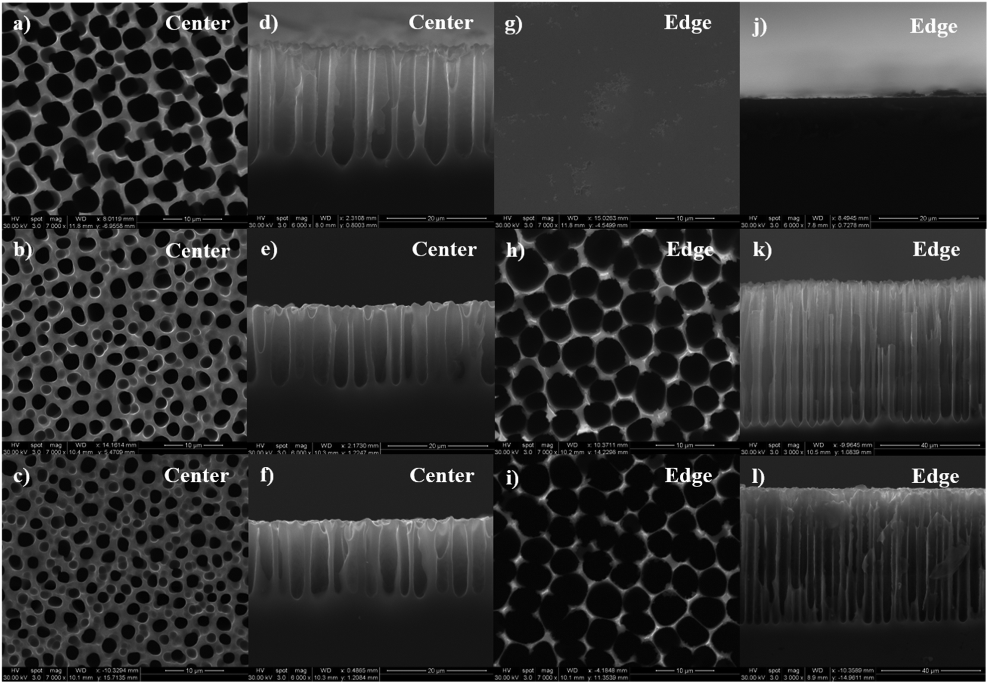 | ||
| Fig. 1 Surface morphology of porous silicon samples prepared using etchant solution containing different amounts of HF. SEM images showing (a)–(c), (g)–(i) top and (d)–(f), (j)–(l) cross-sectional view of porous films at the center and the edge of the samples, respectively. 3E-3% Triton® X-100 and (a), (d), (g), (j) 3% HF, (b), (e), (h), (k) 5% HF and (c), (f), (i), (l) 8% HF aqueous solution were used as etchant solutions, while deposition solution contained 1 M NiSO4 and 0.5 M H3BO3, respectively. Wafer resistivity: 14 Ω cm; current density: 10 mA cm−2. | ||
To better characterize the surface properties of the porous films, a statistical analysis of the SEM images was performed using ImageJ® software to calculate the average pore diameter (davg), porosity (p), average pore depth (havg) and distribution of these parameters across the sample surface. For the center area, an increase in HF concentration from 3% to 5% caused a decrease in the values of davg, havg, and p from 4.0 ± 0.8 μm, 24 ± 3 μm and 54.7% to 2.2 ± 0.4 μm, 15 ± 2 μm and 27.9%, respectively. A further increase in the HF concentration did not cause any significant change in the porous film characteristics with values of davg, havg, and p calculated to be 2.1 ± 0.3 μm, 20 ± 1 μm and 21.1%. At the edge of the sample, the use of 3% HF solution did not result in any pore formation and both 5% and 8% HF solutions exhibited a roughly similar pore diameter and depth and porosity, where the values of davg, havg, and p were computed as 4.6 ± 1.0 μm, 50 ± 2 μm and 68.5% for 5% HF, and 4.7 ± 0.9 μm, 53 ± 2 μm and 75.2% for 8% HF. The distributions of porosity, pore diameter and depth along the diameter of the sample for different HF concentrations are plotted and shown in Fig. 2. As can be seen from Fig. 2(a) and (b), an increase in both pore diameter and depth distribution was observed with increasing HF concentration from 3% to 5%. Also, 5% and 8% HF samples exhibit a similar distribution range for pore dimensions, about 1.5 to 6 μm for the pore diameter and 13 to 60 μm for pore depth. The porosity values shown in Fig. 2(c) indicate that both highest (76%) and lowest porosity (21%) were observed for 8% HF solution and the porosity range reduced with decreasing HF concentration, suggesting that a sharper slope of the porosity gradient was developed with higher concentrations of HF.
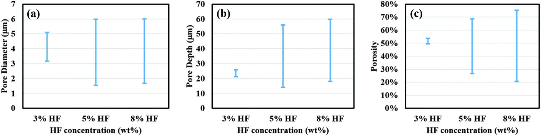 | ||
| Fig. 2 Comparison of surface parameters for porous films obtained using etchant solution containing 3%, 5% and 8% HF. Plots for (a) pore diameter, (b) pore depth and (c) porosity distribution of porous films prepared using different concentrations of HF in etchant solution. Other experimental conditions were same as those used to obtain the data shown in Fig. 1. | ||
The occurrence of electropolishing on samples prepared using 3% HF solutions could be explained based on the design of our geometry. In our system, a radially symmetric current density gradient develops across the sample area, where the current density increases from the center to the edge of the sample. Porous silicon formation will occur only at lower current densities and the surface will get electropolished above a critical value of the current density.29 It has been verified that lower concentration of HF allows electropolishing to occur at smaller current density values, which means that compared to 5% and 8% HF treated samples, the outer area of the 3% HF treated sample is easier to get electropolished.29
In our process, silicon undergoes a two-step dissolution: the first one being electrochemical oxidation to silicon dioxide and the second one involves chemical etching of the oxide.23 The oxidation rate of silicon is determined by the availability of oxidizing agents and current density applied, while the etch rate depends on the concentration and type of fluorine based species in the etchant solution. To understand the etching mechanism, the effect of etchant solution pH and different fluorine species on the oxide etch rate and porous silicon formation was investigated using 5% HF solution containing 3E-3% Triton® X-100 at pH 3.2 (original pH), 4.2 and 6.5. Solution pH was adjusted by adding a small amount of KOH. As shown in Fig. 3(a) through (d), no pore formation was observed for samples prepared using etchant solutions at pH 4.2 and 6.5, although there is some indication of pore initiation for the case of lower pH (4.2). By contrast, pores were fully developed when the HF solution pH was 3.2 (Fig. 1(b), (e), (h) and (k)). Interestingly, the sample surfaces at these two higher pH values did not appear to be electropolished either. Therefore, equilibrium concentrations of various fluorine species in HF solution were established to investigate this pH effect.30 The possible reactions of fluorine species occurring in HF based etchant solution along with the mass balance equation are given in (R1) through (R4).31 The concentrations of different forms of fluorine based species (HF, H2F2, HF2− and F−) have been plotted as a function of etchant solution pH at room temperature and shown in Fig. 4. It can be observed that with increase in solution pH from 3.2 to 4.2, the relative concentration of H2F2 decreased from about 20% to 2%, while HF2− concentration remained unchanged (about 30%); a further increase in the pH value from 4.2 to 6.5 decreased both the concentration of H2F2 and HF2− to almost zero and the solution was dominated by F−.
| HF = H+ + F−; K1 = 6.85 × 10⁻⁴ mol l−1 | (R1) |
| HF + F− = HF2−; K2 = 3.963 l mol−1 | (R2) |
| 2HF = H2F2; K3 = 2.7 l mol−1 | (R3) |
| [HF] + [F−] + 2[HF2−] + 2[H2F2] = 2.5 mol l−1 | (R4) |
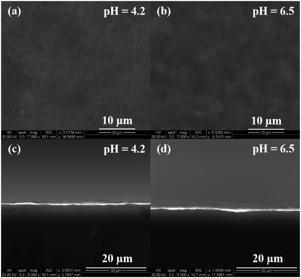 | ||
| Fig. 3 Surface morphology of porous silicon samples prepared using etchant solution of different pH. SEM images showing (a) and (b) top view and (c) and (d) cross-sectional view of porous films. pH of etchant solution: (a) and (c): 4.2, (b) and (d): 6.5. Etchant solution: 5% HF and 3E-3% Triton® X-100 aqueous solution. Deposition solution: 1 M NiSO4 and 0.5 M H3BO3. Wafer resistivity: 14 Ω cm; current density: 10 mA cm−2. | ||
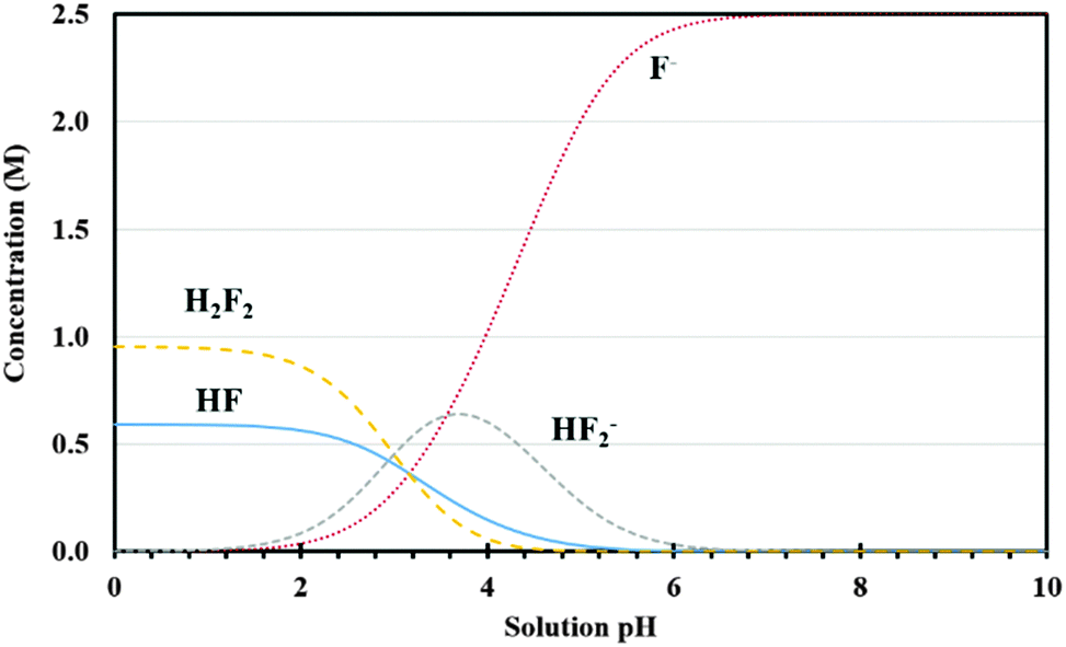 | ||
| Fig. 4 Equilibrium concentrations of various fluorine species as a function of solution pH for total F of 2.5 M at room temperature. | ||
The pore formation is initiated by the valence band holes which are driven to the silicon surface due to applied electric field and diffusion.32 At this initiation stage, the charge carriers are collected by the pore tips with an enhanced electric field. Electrochemical oxidation of silicon preferably originates at the pore tips and surface irregularities and then dissolution of silicon dioxide occurs in those regions due to chemical etching. For samples prepared at a lower etch rate (lower HF concentration or higher pH), fresh silicon surfaces cannot be regenerated in time at pore tips by chemical etching and therefore, in order to ensure the electron transfer rate corresponding to the applied current density, more area on the silicon surface gets oxidized, which leads to etching of the pore sidewalls and widening of pores. Consequently, when 3% HF is used, the pore size is larger and pores are shallower due to sidewall etching; at the edge of the sample, due to higher current density, all the silicon surface in that area gets oxidized, thereby causing uniform etching of the surface. For samples prepared using 5% and 8% HF solutions, the etch rate is high enough at the given oxidation rate (predetermined by the current density), and therefore the porous films show similar distribution of morphology characteristics with the sample prepared using 8% HF (a higher etch rate compared to that at 5% HF) presenting slightly sharper gradient from the center to the edge. In the case of etchant solutions with higher pH (4.2 and 6.5), the etch rate of silicon dioxide experiences a significant reduction perhaps due to decrease in H2F2 concentration, suggesting that H2F2 is a critical species in promoting oxide etch rates. As a result, most of the silicon surface is covered with the oxide film at higher pH, and pores cannot be developed due to non-selective etching.
In addition, the effect of current density (3 and 10 mA cm−2) on porous silicon formation was examined to verify the proposed mechanism using 8% HF and 3E-3% Triton® X-100 in the etchant solution. As shown in Fig. 5(a) through (d), a morphological gradient was successfully developed for the samples obtained at lower current density. In comparison, a slight increase in porosity, pore diameter and depth was measured at the center for samples prepared at higher current density (Fig. 5(e) and (f) versus (a) and (b)). Values of davg, havg, and p at the center increased from 1.9 ± 0.3 μm, 11 ± 2 μm and 18.6% to 2.1 ± 0.3 μm, 20 ± 1 μm and 21.1%, respectively, with an increase in current density from 3 to 10 mA cm−2. When moving from the center to the edge, a notable difference in surface morphology can be observed between samples prepared at lower and higher current density. Values of davg, havg, and p were computed to be 3.1 ± 0.9 μm, 34 ± 2 μm and 61.3% for 3 mA cm−2, and 4.7 ± 0.9 μm, 53 ± 2 μm and 75.2% for 10 mA cm−2, respectively. These results indicate a sharp increase in pore dimensions with increasing current density. It may be important to point out that at lower current density, the actual porous film at the edge of the sample was formed beneath a thin porous layer consisting of larger pores. The distributions of porosity, pore diameter and depth along the entire sample surface are plotted in Fig. 6 to further demonstrate our observations. As shown in Fig. 6(a) through (c), samples prepared at 10 mA cm−2 exhibit a much larger distribution range for all surface parameters compared to those at 3 mA cm−2. Since the applied current density determines the electron transfer rate, which corresponds to the number of silicon atoms dissolved per unit time, applying higher current density can be expected to remove more silicon from the substrate and thereby causes higher porosity and forms larger and deeper pores.
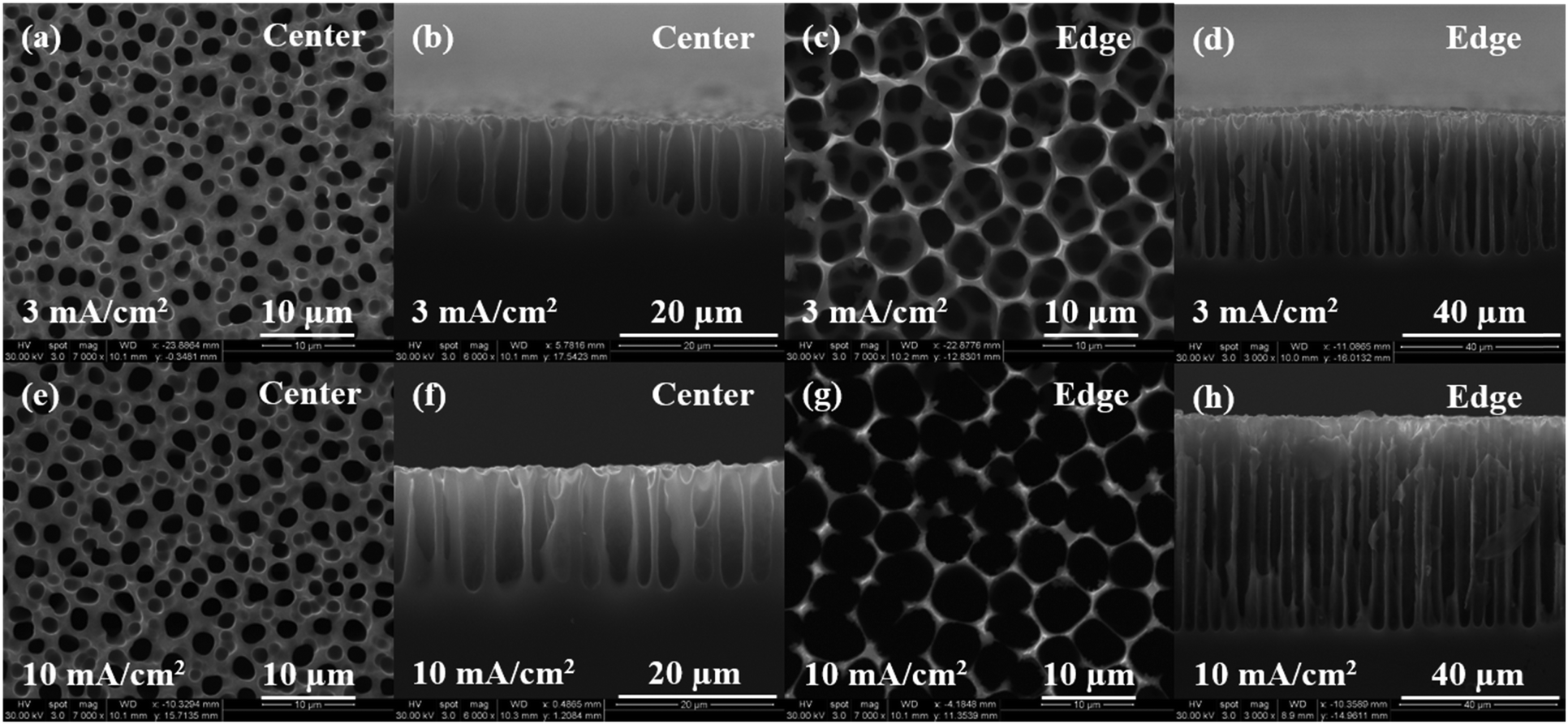 | ||
| Fig. 5 Surface morphology of porous silicon samples prepared with current density of (a)–(d) 3 mA cm−2 and (e)–(h) 10 mA cm−2. SEM images showing (a), (c), (e), (g) top view and (b), (d), (f), (h) cross-sectional view of porous films. Etchant solution: 8% HF and 3E-3% Triton® X-100 aqueous solution. Deposition solution: 1 M NiSO4 and 0.5 M H3BO3. Wafer resistivity: 14 Ω cm. | ||
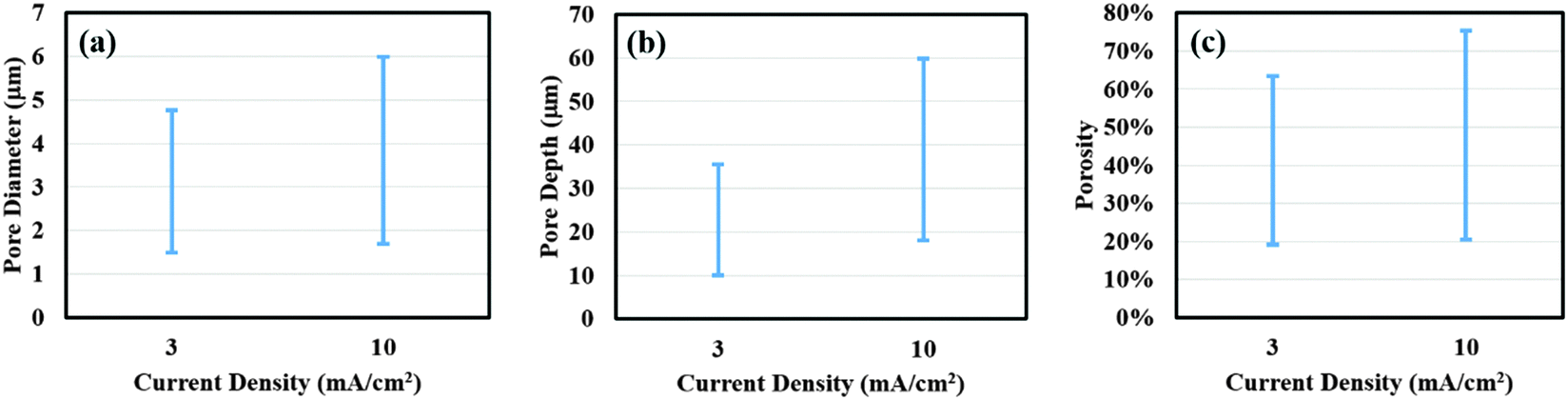 | ||
| Fig. 6 Comparison of surface parameters for porous films obtained using the current density of 3 and 10 mA cm−2. Plots for (a) pore diameter, (b) pore depth and (c) porosity distribution of porous films as a function of different current densities. | ||
In our previous study, we reported that when changing etchant solution composition from 3E-3% Triton® X-100/8% HF/92% H2O to 84% DMSO/8% H2O/8% HF (all by weight), the expected morphological gradient was not developed for samples prepared using DMSO based solutions.24Fig. 7(a), (d), (g) and (j) show the morphology of samples prepared at 3 mA cm−2 using DMSO solution. It is evident that the center and the edge of the sample exhibit similar surface properties. This behavior could be explained based on the availability of oxidizing species at silicon–etchant solution interface. During porous silicon formation, the initial step is to selectively oxidize the pore tips and achieve etching of the oxide to form pores. In the case of samples prepared using DMSO solution, although the etch rate is no longer a problem, the concentration of oxidizing species (which is water here) is too low at the silicon–etchant solution interface to afford the oxidation rate especially at the edge of the sample, where a much greater current density exists than that at the center. Therefore, to maintain the electron transfer rate commensurate to the applied current density, the pore growth rate at the center increases while it decreases at the edge of the sample, as the pores at the center are shallower and easier to get oxidized at the bottom. In this way, a uniform porous layer is developed due to limitations in the oxidation rate at the edge of the sample.
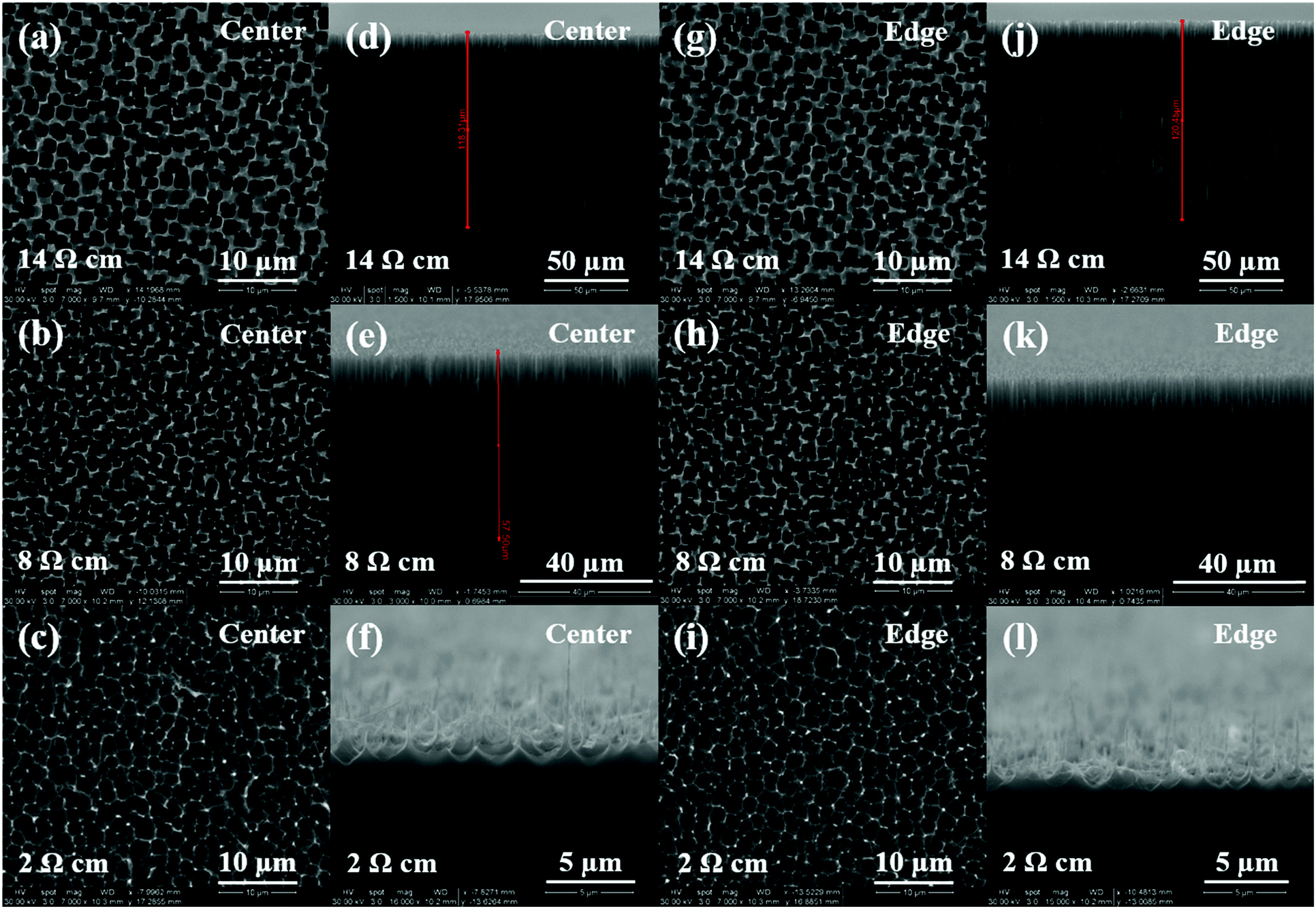 | ||
| Fig. 7 Surface morphology of porous silicon samples prepared using (a), (d), (g), (j) 14 Ω cm, (b), (e), (h), (k) 8 Ω cm and (c), (f), (i), (l) 2 Ω cm wafers. SEM images showing (a)–(c), (g)–(i) top and (d)–(f), (j)–(l) cross-sectional view of porous films at the center and the edge of the samples. Etchant solution: 8% HF, 8% water and 84% DMSO (by weight) solution. Deposition solution: 1 M NiSO4 and 0.5 M H3BO3. Current density: 3 mA cm−2. | ||
To further confirm this observation, we conducted experiments using 84% DMSO/8%H2O/8%HF as the etchant solution on silicon wafers with varying resistivity (2 and 8 Ω cm) at 3 mA cm−2. The resulting SEM images are shown in Fig. 7. Comparing images in different columns of Fig. 7, one may notice that silicon samples with fixed resistivity exhibit a similar surface morphology at the center and the edge of the surface. The pore diameter and depth as a function of wafer resistivity are plotted in Fig. 8. As can be seen from this figure, a decrease in pore diameter and an increase in pore depth were observed with increasing wafer resistivity. In porous silicon formation, the depletion region in the semiconductor also known as the space charge layer prevents the pore sidewalls from being etched. The thickness of the space charge layer is determined by the doping density, where an increase in doping density decreases both the wafer resistivity and thickness of the space charge layer.16 A thinner space charge layer will reduce the focusing effect of charge carriers towards the pore tips, resulting in larger pore formation. Since a constant current density was applied for the same period of time in all cases, an equal amount of silicon should be removed from each sample. Therefore porous films with lower resistivity and larger pores lead to shallower pore formation.
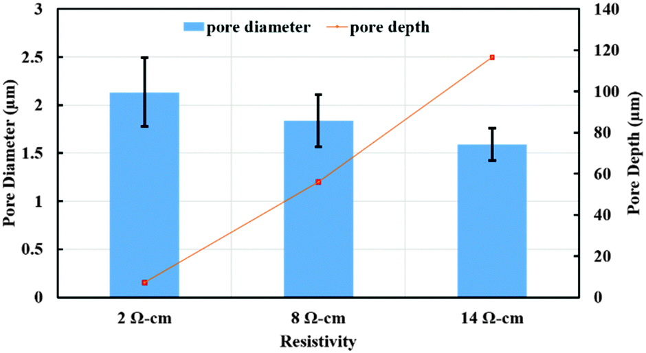 | ||
| Fig. 8 Effect of wafer resistivity on pore diameter and pore depth with an applied current density of 3 mA cm−2. 8% HF/8% H2O/84% DMSO as the etchant solution and 1 M NiSO4 with 0.5 M H3BO3 as deposition solution. | ||
Conclusions
In the current work, various process parameters such as HF concentration, solution pH, current density and wafer resistivity have been examined to understand the formation mechanism of radially symmetrical gradient porous silicon fabricated using a contactless method. Formation of gradient porous silicon was observed when Triton® X-100 was used as the wetting agent in the etchant solution. Comparisons of the effect of HF concentration indicated that a larger distribution range of porosity, pore diameter and depth can be obtained at higher HF concentration (8%), while 3% HF concentration showed narrower distribution with the outer area being electropolished. Increase in the solution pH from 3.2 to 6.5 eliminated the formation of pores on the wafer surface. Subsequent equilibrium calculations indicated a sharp decrease in H2F2 concentration with increase in etchant solution pH, suggesting that lower etch rates of SiO2 at higher pH and lower HF concentration limit the formation of pores. The effect of current density was also evaluated and gradient porous silicon was successfully fabricated at both low and high current densities in the presence of Triton® X-100. An increase in porosity, pore diameter and depth was observed both at the center and the edge of samples as current density increased from 3 to 10 mA cm−2. When using DMSO in the etchant solution, the morphological gradient was not developed along the sample surface. Instead, a uniform porous layer was formed due to limitations in the oxidation rate, which was caused by the restriction in the diffusion of the oxidizing species.Acknowledgements
The authors would like to thank Applied Materials, Inc. for partial support of this work (account # 5510810).Notes and references
- R. L. Smith and S. D. Collins, J. Appl. Phys., 1992, 71, R1–R22 CrossRef CAS.
- S. P. Low, N. H. Voelcker, L. T. Canham and K. A. Williams, Biomaterials, 2009, 30, 2873–2880 CrossRef CAS PubMed.
- A. G. Cullis, L. T. Canham and P. D. J. Calcott, J. Appl. Phys., 1997, 82, 909–965 CrossRef CAS.
- J. Salonen and V.-P. Lehto, Chem. Eng. J., 2008, 137, 162–172 CrossRef CAS.
- A. M. Rossi, L. Wang, V. Reipa and T. E. Murphy, Biosens. Bioelectron., 2007, 23, 741–745 CrossRef CAS PubMed.
- S. M. Prokes, J. Mater. Res., 1996, 11, 305–320 CrossRef CAS.
- V. Lehmann, W. Honlein, H. Reisinger, A. Spitzer, H. Wendt and J. Willer, Thin Solid Films, 1996, 276, 138–142 CrossRef CAS.
- R. Angelucci, A. Poggi, L. Dori, G. C. Cardinali, A. Parisini, A. Tagliani, M. Mariasaldi and F. Cavani, Sens. Actuators, A, 1999, 74, 95–99 CrossRef CAS.
- A. Uhlir, Bell Syst. Tech. J., 1956, 35, 333–347 CrossRef CAS.
- D. Turner, J. Electrochem. Soc., 1958, 105, 402–408 CrossRef CAS.
- H. Foll, M. Christophersen, J. Carstensen and G. Hasse, Mater. Sci. Eng., R, 2002, 39, 93–141 CrossRef.
- T. Unagami, J. Electrochem. Soc., 1980, 127, 476–483 CrossRef CAS.
- R. L. Smith, S. F. Chuang and S. D. Collins, J. Electron. Mater., 1988, 17, 533–541 CrossRef CAS.
- X. G. Zhang, S. D. Collins and R. L. Smith, J. Electrochem. Soc., 1989, 136, 1561–1565 CrossRef CAS.
- V. Parkhutik, Solid-State Electron., 1999, 43, 1121–1141 CrossRef CAS.
- A. Langner, F. Muller and U. Gosele, in Molecular- and Nano-tubes, ed. O. Hayden and K. Nielsch, Springer Science Business Media, New York, 2011, ch. 13, pp. 431–460 Search PubMed.
- V. Lehmanna and S. Rönnebeck, J. Electrochem. Soc., 1999, 146, 2968–2975 CrossRef.
- S. Lust and C. C. Lévy-Clément, J. Electrochem. Soc., 2002, 149, C338–C344 CrossRef CAS.
- Y. H. Ogata, A. Koyama, F. A. Harraz, M. S. Salem and T. Sakka, Electrochemistry, 2007, 75, 270–272 CrossRef CAS.
- K. Chao, S. Kao, C. Yang, M. Hseu and T. Tsai, Electrochem. Solid-State Lett., 2000, 3, 489–492 CrossRef CAS.
- G. M. O'halloran, M. Kuhl, P. J. Trimp and P. J. French, Sens. Actuators, A, 1997, 61, 415–420 CrossRef.
- A. G. Cullis, L. T. Canham and P. D. J. Calcott, J. Appl. Phys., 1997, 82, 909–965 CrossRef CAS.
- M. Zhao, R. Balachandran, J. Allred and M. Keswani, RSC Adv., 2015, 5, 79157–79163 RSC.
- M. Zhao and M. Keswani, Sci. Rep., 2016 Search PubMed , in press.
- P.-Y. Wang, W.-B. Tsai and N. H. Voelcker, Acta Biomater., 2012, 8, 519–530 CrossRef CAS PubMed.
- P.-Y. Wang, L. R. Clements, H. Thissen, A. Jane, W.-B. Tsai and N. H. Voelcker, Electrochem. Adv. Funct. Mater., 2012, 22, 3414–3423 CrossRef CAS.
- S. Ilyas and M. Gal, Appl. Phys. Lett., 2006, 89, 211123 CrossRef.
- C. Xu, X. Zhang, K. Tu and Y. Xie, J. Electrochem. Soc., 2007, 154, D170–D174 CrossRef CAS.
- X. G. Zhang, J. Electrochem. Soc., 2004, 151, C69–C80 CrossRef CAS.
- R. Govindarajan, M. Keswani and S. Raghavan, Mater. Sci. Semicond. Process., 2014, 27, 390–396 CrossRef CAS.
- M. Zhao, R. Balachandran, Z. Patterson, R. Gouk, S. Verhaverbeke, F. Shadman and M. Keswani, RSC Adv., 2015, 5, 45291–45299 RSC.
- M. J. Sailor, Porous silicon in practice: preparation, characterization and applications, Wiley-VCH, Weinheim, 2012 Search PubMed.
| This journal is © The Royal Society of Chemistry 2016 |