
 Open Access Article
 This Open Access Article is licensed under a Creative Commons Attribution-Non Commercial 3.0 Unported Licence
Chemical epitaxy and interfacial reactivity in solution deposited PbS on ZnTe
Sucheta
Sengupta†
a,
Tzvi
Templeman†
a,
Chihyu
Chen
b,
Eunseong
Moon
b,
Michael
Shandalov
c,
Vladimir
Ezersky
a,
Jamie
Phillips
b and
Yuval
Golan
a
aDepartment of Materials Engineering and the Ilse Katz Institute for Nanoscale Science and Technology, Ben-Gurion University of the Negev, Beer-Sheva 84105, Israel. E-mail: ygolan@bgu.ac.il
bDepartment of Electrical Engineering and Computer Science, The University of Michigan, Ann Arbor, Michigan 48109, USA
cDepartment of Physics, Nuclear Research Centre Negev, Israel
First published on 5th February 2016
Abstract
Despite their promise, the efficiency of quantum dot solar cells is currently low (<10%), where an improved understanding of interfaces and contact layers adjacent to the quantum dots is presently a major limitation. The present work aims at optimizing the conditions for growing PbS thin films on ZnTe in light of the solubility of ZnTe in the alkaline environment required for chemical bath deposition of PbS. The morphology and properties of these films are strongly affected by altering the solution pH, temperature and the reagent concentrations. A detailed structural and chemical analysis reveals the different orientation relationships present between the constituent layers and highlights the spontaneous formation of new, distinct intermediate layers in the unique local environment formed due to the simultaneous dissolution of the ZnTe layers in the presence of precursors for PbS thin film deposition.
Introduction
Lead chalcogenides have been the subject of considerable earlier research due to their unique optical and electronic properties and their technological importance for infrared radiation detection and emission and solar cells.1,2 Lead chalcogenide quantum dots are particularly suitable for incorporation into energy conversion architectures and are fundamentally interesting in light of their unusual photophysics.3,4 Analysis of the natural abundance of materials for solar cells shows that bulk PbS ranks favorably in terms of the cost and abundancy of raw materials.5 Of the several techniques for fabricating high quality PbS thin films, chemical bath deposition is one of the simplest and cost effective methods. Chemically deposited PbS thin films can be easily integrated on almost any substrate and their band gap energy can be tuned from 0.41 eV of the bulk material to 0.8 eV in a shorter wavelength depending on the grain size due to the quantum confinement effect.6–10 PbS is a good alternative to other narrow band gap semiconductors for integration in electric and optoelectronic devices due to its relatively large Bohr radius of 18 nm so that quantum confinement effects can take place at a relatively large grain size.Among alternative approaches to improve the efficiency of photovoltaic devices, the most notable is the multi-junction (MJ) solar cell.11–13 MJ devices consist of stacked semiconductor junctions built in tandem; thus, material band gaps are tuned across a wide range of wavelengths in the solar spectrum. Since the constituent junctions can efficiently extract power from the different portions of the solar spectrum, their power conversion efficiency are much higher compared to single junction solar cells. Quantum dot solar cells also show promise, but their power conversion efficiency is currently low (<10%), where an improved understanding of interfaces and contact layers adjacent to the quantum dots is presently a major limitation. Layered structures of nanocrystalline thin films based on PbS quantum dot absorbers, along with electron and hole blocking layers based on compatible II–VI semiconductors, have been recently designed for improved solar cell efficiency.14–16 ZnTe is well suited as a selective contact for holes on one side with properties quite similar to CdTe (a well-established material in thin film solar cell technology) and highly compatible crystalline and electronic structure. Literature reports suggest that the epitaxial growth of PbSe on GaAs (211)B or Si(211) may be achieved using ZnTe as a buffer layer.17,18 Improvement in optical properties, minority carrier lifetimes, and interface quality may be possible using PbSe/ZnTe structures to provide enhancement in solar energy conversion.
Chemical bath deposition (CBD) offers a simple and cost effective method for the fabrication of high quality semiconductor films. Literature reports suggest the growth of epitaxial PbS single crystal films,19,20 where the term chemical epitaxy refers to the presence of a well-defined crystalline relationship between the CBD single crystal film and the substrate. Although epitaxy usually requires a certain degree of lattice match between the semiconductor film and substrate, chemical interactions between the constituents of the deposition and the substrate are often critical. Due to the complexity of the mechanisms in chemical deposition and several competing factors (chemical and structural) among the substrate, film, and the solution, it is difficult to predict a priori the effect of the substrate on the film orientation. The most common deposition mechanisms active in CBD are the cluster mechanism and the ion-by-ion mechanism.21 In the cluster mechanism, the film growth occurs by the migration and adsorption of colloidal particles either of the desired material or of a certain intermediate species. Alternatively, the film growth can also occur by the decomposition of the chemical precursors directly onto the substrate surface, the process commonly known as the ion-by-ion mechanism. Previous studies from our group establish the correlation between the morphological evolution, crystallographic orientation of the thin film and the active deposition mechanisms by varying the different deposition parameters.22–24
To the best of our knowledge, there have been no explicit reports of growing PbS thin films on ZnTe by CBD and exploring their plausible epitaxial relationships. In this work, we have optimized the deposition conditions in order to achieve homogeneous, continuous, and adherent films to serve as the constituent layers of solar cells. The temperature and pH were varied and the structural characteristics examined, with an emphasis on the identification of interfacial phases formed. The morphology and properties of these films were found to be strongly affected by altering the solution pH, temperature and the reagent concentrations. A detailed structural analysis reveals the different epitaxial relationships present between the constituent layers. We also demonstrate that depending on the growth mechanism, the epitaxial relationships are transmitted differently under CBD conditions resulting in films with different crystalline orientations.
Experimental
Materials and chemicals
ZnTe thin films were grown by molecular beam epitaxy (MBE) on Si(100) substrates. The Si(100) substrates were etched with buffered HF prior to loading into the MBE vacuum chamber, and heated to 600 °C to remove the surface native oxide. The in situ removal of the native oxide was confirmed by an observed streaky reflection high-energy electron diffraction pattern. Prior to ZnTe growth, the silicon substrate was exposed to a Zn flux. During epitaxial growth, Zn flux was maintained at a fixed beam equivalent pressure (BEP) value of approximately 1 × 10⁻⁶ Torr and Te flux was varied from 1 × 10⁻⁶ Torr to 5 × 10⁻⁶ Torr (BEP). The typical substrate temperature (Tsub) was 300 °C to 350 °C, with a growth rate of approximately 1 μm h−1.PbS films were deposited on the ZnTe films using the following solution: Pb(NO3)2 as the lead source, CS(NH2)2 as the sulfide source and NaOH as a complexant and pH adjustment reagent, under various conditions of deposition pH and temperature. Lead nitrate (Aldrich, analytical 99+%), thiourea (Aldrich, ACS >99.0%) and sodium hydroxide (Gadot, AR) were used without further purification. The solution contained 8.9 mM Pb(NO3)2, 51 mM CS(NH2)2 and 0.08–0.2 M NaOH (depending on the desired pH) in 18 MΩ distilled water (Millipore Direct Q3). The deposition solutions were prepared by stirring NaOH with distilled water followed by slow addition of PbNO3. Prior to deposition, the solution was purged with UHP N2 gas for 60 min in order to reduce levels of dissolved O2 and CO2. The wafers were cleaved into 2 cm × 1 cm samples, cleaned with ethanol and water and passivated for 10 min in the deposition solution prior to deposition. Typically, deposition was carried out for 180 min at a particular temperature within a thermostatic bath. Film morphology was studied by X-ray diffraction (XRD), high resolution scanning electron microscopy (HR-SEM) and transmission electron microscopy (TEM). The interfacial composition and structure was analyzed using analytical TEM (ATEM).
Characterization methods
TEM and HRTEM were carried out using a JEOL JEM-2100F instrument operating at 200 kV. Selected area electron diffraction (SAED) patterns were obtained by positioning the selected area diffraction aperture of the TEM over the desired area of the films and/or substrate. ATEM investigations including Energy Dispersive Spectroscopy (EDS) analysis in the scanning TEM (STEM) mode were carried out by using a JEOL JEM-2100F analytical TEM operating at 200 kV. Gatan DigitalMicrograph 3 software was used for fast Fourier transform (FFT) analysis of HRTEM lattice images of the PbS/ZnTe interface. Schematic illustrations of the orientation relation models were obtained using CaRine Crystallography software.
where T is the transmittance, I is the transmitted light intensity through the sample cell, I0 is the transmitted light intensity through the reference cell, α is the absorption coefficient and d is the deposited film thickness. A plot of the square of absorption coefficient (α2) versus photon energy (hν) was used to extract the optical bandgap (EG) of the material at the energy axis intercept.
Results and discussion
The deposition conditions for growing PbS semiconducting thin films were optimized on ZnTe thin films on Si substrates. The influence of different deposition parameters such as time, temperature, and reagent concentrations on the morphology of the films was studied. The standard protocol for growing PbS thin film involves moderate pH (the pH of the solution is 13.12) at moderate temperature (20–30 °C) for 120–180 minutes.25 The hydroxide concentration is of utmost importance because elevated pH leads to dissolution of the ZnTe layer. Thus deposition on ZnTe required optimizing the growth conditions for growth at low pH in order to minimize dissolution of the ZnTe layer. The XRD and HRSEM images for the films deposited at various temperatures at a constant pH value of 13.2 are described in Fig. 1(a)–(e). The X-ray diffractograms demonstrate the formation of a [100] textured PbS film at lower deposition temperature (20 °C). With increasing deposition temperature, there is a gradual increase in the (111) peak with the simultaneous decrease in the (200) peak. The plan-view HRSEM images (Fig. 1(a)–(e)) reveal the formation of cubic PbS grains at 20 °C which gradually changes with increasing deposition temperature to form pyramidal PbS grains (the typical topography for a (111) surface in the cubic system), reflecting the change in texturing as observed in XRD.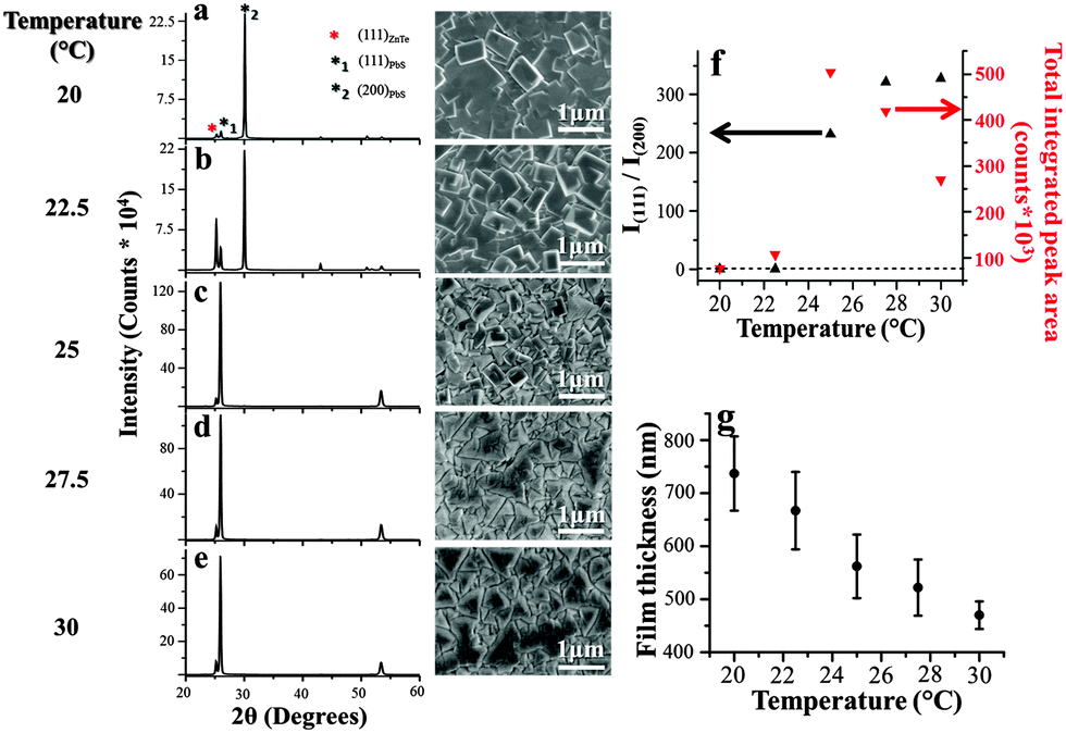 | ||
| Fig. 1 (a–e) X-ray diffractograms and corresponding plan-view HRSEM images for films grown at different temperatures for 180 min. (f) I(111)/I(200) Bragg peak intensity ratio (black) and total integrated peak area (red). The horizontal line indicates the powder ratio. (g) Film thickness observed from cross-sectional HRSEM images. | ||
The variation of the XRD Bragg peak intensity ratio (111)/(200) with temperature is shown in Fig. 1(f). The value at 20 °C (0.05) is much lower than the powder ratio value (0.9), which drastically increases to an exceptionally high value of ∼300 at 30 °C indicating the formation of highly textured films. The total peak area plotted vs. temperature (Fig. 1(f)) shows low values that are slightly increasing for the first two temperatures (20 and 22.5 °C), after which a sharp increase is obtained for the film grown at 25 °C. Thereafter, further increase of the temperature results in a decrease in the total peak area. The variation in film thickness (as observed from the cross-sectional HRSEM images) with temperature is plotted in Fig. 1(g). The film thickness is found to decrease continuously with the increasing temperature. It should be noted that the total peak area and film thickness are expected to follow the same trend. However, the discrepancies at the lower temperatures suggest the formation of amorphous clusters resulting from parallel growth of the cluster mechanism along with the dominant ion-by-ion mechanism, which occurs at lower deposition temperatures.10,21 Another cause of this discrepancy might be the result of disorder in the nanocube film, which may be porous and contain high defect densities as established by TEM. Above 25 °C, both the film thickness and the total integrated XRD peak area are found to decrease with temperature. A possible explanation for this may be that with increasing temperature, the film texturing increases (Fig. 1f) which results in a more compact film with decreasing porosity, leading to the decrease in both the film thickness and the total XRD peak area. Under the current conditions, continuous and adherent films were obtained which may be attributed to considerable lowering of the lattice mismatch with PbS for deposition on ZnTe to ∼1.9%.
The effect of pH on film morphology was subsequently investigated. The XRD and HRSEM images for the films resulting at various NaOH concentrations of the deposition solutions maintaining the deposition temperature at 30 °C is described in Fig. 2(a)–(d). The X-ray diffractograms show that at lower pH, the resultant PbS films are (100) textured. With increasing pH there is a transition in film texturing. Similar to the temperature effect, increasing pH also resulted in a gradual increase in the (111) peak intensity, accompanied by a simultaneous decrease in the (100) peak intensity. The plan-view HRSEM images reveal the formation of cube like PbS grains at pH = 12.9 which gradually changes to form pyramidal PbS grains at pH = 13.1, reflecting the change in texturing observed in XRD. Fig. 2(e) shows the variation of the XRD Bragg peak intensity (111)/(200) vs. pH. A similar trend was observed in Fig. 1(f), where the value is much lower than the powder ratio value for pH 12.9, which drastically increases to an exceptionally high value of ∼300 at pH 13.2 indicating the formation of a highly textured film. The total integrated XRD peak area plotted versus pH (Fig. 2(f)) shows a continuous increase in peak area with pH. In this case, a better correlation was observed between the total peak area and the film thickness (obtained from the cross-sectional HRSEM images) as a function of pH (Fig. 2(f)).
 | ||
| Fig. 2 (a–d) X-ray diffractograms and corresponding plan-view HRSEM images for films grown at different pH values for 180 min and at 30 °C. (e) I(111)/I(200) Bragg peak intensity ratio (black) and total integrated peak area (red). The horizontal line indicates the powder ratio. (f) Film thickness observed from cross-sectional HRSEM images. | ||
In order to evaluate whether well-defined orientation relationships existed between the film and the underlying substrate, cross-sectional TEM samples were prepared for the PbS/ZnTe/Si(100) structure. This was carried out for two different samples, a (111) textured PbS film deposited at 30 °C and a (200) textured PbS film deposited at 20 °C. Understanding the differences in film growth leading to these changes is fundamental for understanding and controlling growth kinetics. For this purpose, selected area electron diffraction (SAED) was performed at various regions of interest and carefully analysed.
The ZnTe films contain large densities of twinning defects, which are quite common in FCC-based structures, especially considering the notable lattice mismatch with the Si substrate (∼11.5%), leading to polycrystalline film morphology. SAED performed on a large number of grains in several ZnTe films reaffirmed XRD indications of film growth along the [111] direction. TEM imaging and SAED data, along with analysis of the film–substrate orientation relationships, are presented in Fig. 3. ZnTe films grown on Si(100) single crystal substrates are preferentially oriented with the (111)ZnTe parallel to the Si substrate surface and [![[1 with combining macron]](https://www.rsc.org/images/entities/char_0031_0304.gif) 10]ZnTe or 10ZnTe are parallel to the electron beam direction, also defined as the zone axis (ZA) of the electron diffraction pattern. The twinning plane was identified as (111)ZnTe.26
10]ZnTe or 10ZnTe are parallel to the electron beam direction, also defined as the zone axis (ZA) of the electron diffraction pattern. The twinning plane was identified as (111)ZnTe.26
 | ||
| Fig. 3 X-TEM micrograph of the PbS/ZnTe/Si(100) layered structure. The Si–ZnTe interfaces were analyzed using SAED in two adjacent locations marked with yellow circles labelled “a” and “b”, depicting two distinct relationships between the film and substrate. (c) SAED of the interface labelled “a”. Inset: Indexing for the diffraction spots obtained for the [01]Si and [01]ZnTe zone axes (ZA). (d) SAED of the interface labelled “b”. Inset: Indexing for the diffraction spots for the [01]Si and [10]ZnTe ZA. Note that the common in-plane direction is the ZA and therefore it cannot be seen in the diffraction patterns. | ||
PbS films grown at 30 °C showed a clear (111) texturing as a result of the epitaxial relationships with the underlying ZnTe film, which is quite expected considering the negligible lattice mismatch of ∼2.5%. TEM analysis confirmed this, revealing the straightforward, conventional orientation relationship between (111)Film||(111)Substrate and 10Film||[10]Substrate as seen in Fig. 4.
 | ||
| Fig. 4 X-TEM micrographs of the PbS/ZnTe/Si(100) structure, with the PbS film grown at 30 °C. (a) Micrograph showing the exact location analyzed using SAED (yellow circle), SAED pattern and indexing for the diffraction spots in the [10]PbS and [10]ZnTe ZA. (b) Micrograph showing the exact location analyzed, SAED and indexing for the diffraction spots in the [10]PbS and [10]ZnTe ZA. | ||
This relationship is kept throughout the film even though ZnTe is twinned in nature, i.e. when a ZnTe lattice is inverted by 180° due to a twin boundary; PbS growth tracks these changes and reverses accordingly in order to maintain the crystalline orientation relationships. This point is emphasized by Dark Field (DF) TEM images generated by the (11)PbS reflection in Fig. 5(b), which coincides with (11)ZnTe reflections from neighbouring grains (diffraction indexing in Fig. 4(a) and (b)). The resulting image (Fig. 5) shows how the PbS film adapts its growth in accordance with the underlying ZnTe grain orientation.
 | ||
| Fig. 5 (a) SAED pattern of the ZnTe–PbS interface presented in Fig. 4, in which the (11)PbS reflection is encircled. (b) Corresponding DF X-TEM micrograph. | ||
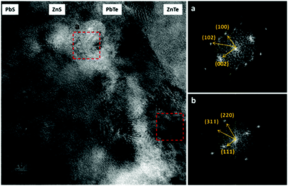
The PbS films grown at 20 °C demonstrate a dramatic difference in structural properties. The XRD results (Fig. 1(a)) showed strong (200) texturing, while integrated scattering intensities do not correlate with film thickness as measured from X-SEM, presumably due to porosity in the films. SAED X-TEM analysis (not shown) confirmed the (200) texturing of the PbS films with no orientation relationships with the underlying ZnTe film, i.e., each PbS grain is randomly oriented with regard to the underlying ZnTe. The root cause is suspected to be at the film interface, which appeared to be nanocrystalline in nature. High Angle Annular Dark Field (HAADF) imaging was carried out in Scanning TEM (STEM) mode combined with EDS to monitor composition variations along the ZnTe–PbS interface. As seen in Fig. 6, the interface is composed of two distinct intermediate layers with dissimilar atomic weight. Moreover, the PbS film was found to be highly defective with pores concentrated at grain boundaries (verified with EDS and encircled in Fig. 6), indicating non-uniform growth where grains are often seen to inhibit growth of adjacent grains. This may explain the conflicting results observed in Fig. 1(f) and (g) between total XRD peak intensity and the film thickness observed from X-SEM images.
 | ||
| Fig. 6 HAADF STEM micrograph of the PbS–ZnTe interface. PbS film was chemically deposited at 20 °C. Porosity located at grain boundaries is marked by a circle. Locations analyzed by EDS are marked a–d. | ||
STEM EDS analyses performed at the locations marked in the figure are presented in Table 1. Interestingly, the interface appears to contain PbTe nanocrystals (region b) above which a very thin layer of fine nanocrystalline ZnS grains is formed (region c). Within the experimental error, regions a and d correspond to ZnTe and PbS layers, respectively.
To verify the presence of solid phases at the interface, HRTEM imaging was performed at several locations along the interface (Fig. 7). Careful FFT analysis at several locations confirms the presence of PbTe (ICDD No. 38-1435) above which ZnS has formed (ICDD No. 36-1450); the data are presented in Table 2.
 | ||
| Fig. 7 High resolution TEM lattice image of a cross-sectional sample deposited at 20 °C. (a, b) Fast Fourier Transform (FFT) obtained from the marked regions labelled (a) and (b). | ||
Note that both phases are nanocrystalline in nature and well-defined orientation relationships between interface layers and films were not observed.
Examining the interface in these samples reveals the dissolution of the ZnTe, an effect which was not observed when PbS films were deposited at T = 30 °C. Once the ZnTe films are immersed in the growth solution they are partially dissolved in the alkali environment; thus, Zn2+ and TeO32− (results from the reaction between the telluride ions with hydroxide) ions are extracted in high local concentrations at the solid–solution interface. PbTe having a drastically lower solubility product (−log(Ksp) = 48, compared to that of ZnTe: 34, ZnS (Sphalerite): 29, ZnS (Wurtzite): 28 and PbS: 29)27,28 is readily formed by consuming the free TeO32− upon the dissolved ZnTe interface. Not surprisingly, the nucleation of PbTe occurs in etch pits that are the energetically preferred sites within the ZnTe surface. Once depleted, the remaining Zn2+ ions compete with solution Pb2+ ions on the available S2−. Although solubility products of PbS and ZnS are quite similar, the high local concentration of Zn2+ can explain the tendency to form the latter.
These effects are absent for cases where (111) textured PbS was grown by implementing high pH or temperature in the solution, indicating a kinetic nature. Once ZnTe is immersed in the solution, two competing mechanisms take place: dissolution of the ZnTe film and growth of PbS; growth conditions containing higher pH or temperatures lead to rapid PbS nucleation, thus coating and protecting the ZnTe films from dissolution. The opposite is true in cases where lower pH or temperatures are used; PbS nucleation is slower and the ZnTe film remains exposed and is subject to dissolution. This retarded nucleation at lower pH or temperature was also evidenced from an interrupted growth series of chemically deposited PbS films on ZnTe on Si with growth terminated after 10, 20, and 30 min. The resulting samples were studied using plan-view HRSEM and XRD. At lower pH (pH 13), there is no formation of PbS after 10 and 20 min. Both XRD and HRSEM showed the presence of only MBE grown ZnTe film. After 30 min, there is formation of a discontinuous ∼100 nm thick layer of PbS with preferred texturing along the 〈100〉 direction (Fig. 8a–c). At higher pH 13.1, the PbS formation rate is increased with an initial layer of ∼65 nm of PbS with random texturing being formed after 20 min of the initiation of the reaction. Moreover, initial formation of PbS is indicated by XRD after 10 min from the commencement of the reaction. After 30 minutes, there is formation of a ∼200 nm thick PbS layer with strong texture along the 〈111〉 direction (Fig. 8(d)–(f)).
 | ||
| Fig. 8 HRSEM plan-view and cross-sectional images and XRD patterns showing the formation of PbS films deposited at 30 °C for 30 min at pH 13 (a–c) and pH 13.1 (d–f). The dotted line in (b) and (e) indicates the interface between the ZnTe and PbS layers. Red asterisks indicate the ZnTe phase and blue asterisks indicate the PbS phase. | ||
Optical transmittance spectra were recorded in near-IR and Mid-IR range on the various samples deposited at different temperatures, pH and deposition times using FTIR. One limitation of the FTIR measurement is that the irregular surface of the samples results in diffuse reflectance rather than specular reflectance, interfering with the reflectance measurement from FTIR. Nevertheless, plots of the absorption coefficient obtained from direct transmittance demonstrate clear onset points in optical absorption to reveal a defined optical bandedge. The results of extracted α2versus hν and the resulting extracted bandedge are shown in Fig. 9. All samples deposited at 30 °C (deposited for 180 min as the thin film samples described above, as well as thicker films deposited for 360 min) demonstrate a consistent bandedge in the range of 0.41–0.44 eV. These values show a good agreement with the bandgap values of bulk PbS.7 However, the sample deposited at 0 °C has a nano-spherical microstructure (not shown) and correspondingly shows larger bandedge energy due to quantum confinement, and a relatively poor optical bandedge characteristic, consistent with structural properties.
 | ||
| Fig. 9 A plot of photon energy (hν) vs. the second power of absorption coefficient (α2) of various PbS samples obtained from FTIR. Bandgap values (Eg) of PbS samples deposited at different temperatures, pH and deposition times are estimated by extrapolating the dashed lines at α2 = 0 along the linear regions of the curves. | ||
Conclusions
In conclusion, uniform PbS thin films were successfully deposited over intermediate MBE grown ZnTe films on Si wafers. The morphology and properties of these films are strongly affected by the solution pH, temperature, and the reagent concentrations. The variation in film morphology and texturing can be related to the presence of two different growth mechanisms involved. At higher temperature or higher pH, when there is direct deposition of PbS, the orientation relationship is dictated by the substrate with the PbS growing epitaxially on the 〈111〉 textured ZnTe. With lowering the temperature or the pH, delayed nucleation of the PbS film results in partial dissolution of the ZnTe layer and losing the epitaxial relationships, leading to controlled deposition in the thermodynamically favored orientation along the 〈100〉 direction. The structural and compositional characteristics of the interfaces are critical for future use in solar cells or related optoelectronic devices. Specifically if dissolution of ZnTe occurs, unavoidable interfacial defects are expected to be present at the heterojunctions, which are likely to produce defect states in the forbidden bandgap. Both band bending effects and the recombination of excess minority carriers can be expected as a consequence. Moreover, in cases where intermediate layers were formed, critical device failure may be expected due to strong band bending and the highly defective nature of the intermediate layers. Controlling the PbS nucleation rate versus ZnTe dissolution rate will be critical in optimizing device structures for optoelectronic device applications.Acknowledgements
We thank Dr Dmitry Mogilyansky for expert assistance in XRD. This research was carried out in the framework of the Energy Initiative Program and supported by the Adelis Foundation for renewable energy research, and by the Israel Science Foundation under Grant #156/14. S. S. G. acknowledges a postdoctoral fellowship from the Planning and Budgeting Committee of the Israeli Council for Higher Education.References
- P. K. Nair, M. T. S. Nair, A. Fernandez and M. Ocampo, J. Phys. D: Appl. Phys., 1989, 22(6), 829 CrossRef CAS.
- P. K. Nair and M. T. S. Nair, J. Phys. D: Appl. Phys., 1990, 23(2), 150 CrossRef CAS.
- K. D. Dobson, G. Hodes and Y. Mastai, Sol. Energy Mater. Sol. Cells, 2003, 80(3), 283–296 CrossRef CAS.
- P. K. Nair, M. Ocampo, A. Fernandez and M. T. S. Nair, Sol. Energy Mater., 1990, 20(3), 235–243 CrossRef CAS.
- C. Wadia, A. P. Alivisatos and D. M. Kammen, Environ. Sci. Technol., 2009, 43(6), 2072–2077 CrossRef CAS PubMed.
- M. P. Hansen and D. S. Malchow, Proc. SPIE, 2008, 6939, 69390I CrossRef.
- A. Osherov, J. P. Makai, J. Balazs, Z. J. Horvath, N. Gutman, A. Sa'ar and Y. Golan, J. Phys.: Condens. Matter, 2010, 22(26), 262002 CrossRef PubMed.
- T. Safrani, T. A. Kumar, M. Klebanov, N. Arad-Vosk, R. Beach, A. Sa'ar, I. Abdulhalim, G. Sarusi and Y. Golan, J. Mater. Chem. C, 2014, 2(43), 9132–9140 RSC.
- A. Osherov, V. Ezersky and Y. Golan, J. Cryst. Growth, 2007, 308(2), 334–339 CrossRef CAS.
- A. Osherov and Y. Golan, Phys. Status Solidi C, 2008, 5(11), 3431–3436 CrossRef CAS.
- D. A. R. Barkhouse, R. Debnath, I. J. Kramer, D. Zhitomirsky, A. G. Pattantyus-Abraham, L. Levina, L. Etgar, M. Grätzel and E. H. Sargent, Adv. Mater., 2011, 23(28), 3134–3138 CrossRef CAS PubMed.
- I. J. Kramer and E. H. Sargent, ACS Nano, 2011, 5(11), 8506–8514 CrossRef CAS PubMed.
- J. Tang and E. H. Sargent, Adv. Mater., 2011, 23(1), 12–29 CrossRef CAS PubMed.
- O. E. Semonin, J. M. Luther and M. C. Beard, Mater. Today, 2012, 15(11), 508–515 CrossRef CAS.
- J. Gao, J. M. Luther, O. E. Semonin, R. J. Ellingson, A. J. Nozik and M. C. Beard, Nano Lett., 2011, 11(3), 1002–1008 CrossRef CAS PubMed.
- J. M. Luther, J. Gao, M. T. Lloyd, O. E. Semonin, M. C. Beard and A. J. Nozik, Adv. Mater., 2010, 22(33), 3704–3707 CrossRef CAS PubMed.
- X. J. Wang, Y. B. Hou, Y. Chang, C. R. Becker, R. F. Klie, R. Kodama, F. Aqariden and S. Sivananthan, J. Cryst. Growth, 2010, 312(7), 910–913 CrossRef CAS.
- X. J. Wang, Y. Chang, Y. B. Hou, C. R. Becker, R. Kodama, F. Aqariden and S. Sivananthan, J. Vac. Sci. Technol., A, 2011, 29(5), 051503 Search PubMed.
- J. L. Davis and M. K. Norr, J. Appl. Phys., 1966, 37(4), 1670–1674 CrossRef CAS.
- M. Isshiki, T. Endo, K. Masumoto and Y. Usui, J. Electrochem. Soc., 1990, 137(9), 2697–2700 CrossRef CAS.
- G. Hodes, Chemical Solution Deposition of Semiconductor films, Marcel Dekker, Inc., New York, 2002 Search PubMed.
- A. Osherov, M. Shandalov, V. Ezersky and Y. Golan, J. Cryst. Growth, 2007, 304(1), 169–178 CrossRef CAS.
- A. Osherov, V. Ezersky and Y. Golan, Cryst. Growth Des., 2012, 12(8), 4006–4011 CAS.
- A. Osherov and Y. Golan, MRS Bull., 2010, 35(10), 790–796 CrossRef CAS.
- A. Osherov, V. Ezersky and Y. Golan, J. Cryst. Growth, 2007, 308(2), 334–339 CrossRef CAS.
- A. Kelly and K. M. Kevin, Crystallography and crystal defects, Wiley, 2nd edn, 2012 Search PubMed.
- H. L. Clever and F. J. Johnston, J. Phys. Chem. Ref. Data, 1980, 9(3), 751–784 CrossRef CAS.
- H. L. Clever, M. E. Derrick and S. A. Johnson, J. Phys. Chem. Ref. Data, 1992, 21(5), 941–1004 CrossRef CAS.
Footnote |
| † These authors contributed equally to this work. |
| This journal is © The Royal Society of Chemistry 2016 |