
 Open Access Article
 This Open Access Article is licensed under a
 Creative Commons Attribution 3.0 Unported Licence
Screening procedure for structurally and electronically matched contact layers for high-performance solar cells: hybrid perovskites†
Keith T.
Butler
*a,
Yu
Kumagai
b,
Fumiyasu
Oba
bcd and
Aron
Walsh
ae
aCentre for Sustainable Chemical Technologies and Department of Chemistry, University of Bath, Claverton Down, Bath BA2 7AY, UK. E-mail: k.t.butler@bath.ac.uk
bMaterials Research Center for Element Strategy, Tokyo Institute of Technology, Yokohama 226-8503, Japan
cMaterials and Structures Laboratory, Tokyo Institute of Technology, Yokohama 226-8503, Japan
dCenter for Materials Research by Information Integration, National Institute for Materials Science, Tsukuba 305-0047, Japan
eGlobal E3 Institute and Department of Materials Science and Engineering, Yonsei University, Seoul 120-749, Korea
First published on 8th January 2016
Abstract
The rapid progress in performance of solar cells based on hybrid halide perovskites means that devices based on these materials have reached a stage where research interest can now focus on development of robust technology. One of the key questions relating to these (and indeed any) devices is their lifetime and stability which in turn is often influenced by the quality of interfaces and junctions within the device. In this study we present a methodology which allows screening for mechanically stable, electronically suitable interface combinations – applying the technique to screen 175 common semiconductors for viability as electron and hole extracting contacts for CH3NH3PbI3. The screening method can be applied to any semiconductor junction problem and relies on easily obtained experimental or theoretical information – electron affinity, ionisation potential, lattice parameters and crystal structure. From the screening we rank the candidates according to a figure of merit, which accounts for band alignment and chemical/mechanical stability of the interface. Our screening predicts stable interfaces with commonly applied electron extraction layers such as TiO2 and ZnO as well giving insight into the optimal polymorphs, surfaces and morphologies for achieving good quality contacts. Finally we also predict potentially effective new hole and electron extraction layers, namely Cu2O, FeO, SiC, GaN, and ZnTe.
I. Introduction
Solution processed hybrid halide perovskite solar cells have recently emerged as highly efficient, cost effective alternative for photovoltaic energy production.1–4 Recently cells based on APbX3, where A is an organic cation (predominantly CH3NH3 or NH2CHNH2) and X is a halide (Cl, Br or I) have surpassed 20% efficiency5 making them competitive (in terms of efficiency) with mature technologies such as Si and CdTe. Devices based on hybrid perovskites however, have thus far proved too unstable to be considered a viable technological alternative to existing cells.6To date most of the research on hybrid perovskite solar cells has focused on the optimisation of the absorber layer. However, device optimisation also requires close attention be paid to contacting materials (for charge extraction) and the interfaces between materials. Indeed, single crystals have been found to have extraordinarily long carrier lifetime7 and it has been noted in several studies that the majority of efficiency loss in hybrid perovskite devices is related to electron–hole recombination in the interface region.8,9 In more mature technologies such as c-Si solar cells a lot of attention has been paid to the effects of orientation,10 doping11 and strain12 at interfaces. The challenge of designing new contact layers must address two crucial parameters: (i) good alignment of electronic energies at the interface,13 to allow for efficient charge extraction, while minimising energy loss; (ii) robust mechanical contacts with minimal interfacial defects, to ensure maximal durability and minimise interface carrier recombination sites.
Typical hybrid perovskite cells have been based on TiO2 electron extraction contacts and Spiro-oMeTAD hole extraction contacts.14,15 Empirically this architecture has been found to give the optimal efficiency although stability remains a concern.16 Nonetheless, based on the principles outlined above it is possible to imagine a host of alternative architectures with the potential to improve stability and device performance. Recently electron contacts based on ZnO17–20 and all solid-state inorganic cells with CuI hole extraction layers21 have been reported. In the case of the latter cells lifetimes and cyclability were found to be significantly improved by the inclusion of the CuI layer. There has also been active research for improved organic hole extraction materials, with modular analouges predicted to give improved band offsets with the absorber layer.22
The choice of contacting semiconductors is almost endless and the ability to efficiently screen potential candidates, based on easily obtained experimental or theoretical parameters would allow for a significant reduction in the trial-and-error studies required to establish new combinations. In this contribution we outline such a methodology and apply our scheme to a set of 175 semiconducting materials, identifying 17 candidate hole or electron contacts. Encouragingly our method predicts the solid-state materials most commonly applied in halide perovskite devices (organic materials are beyond the scope of the current methodology) as well as highlighting potential superior alternatives.
Interfacial phenomena can become extremely complicated and it is becoming clear that effects such as local ordering of dipoles23–25 and the role of chemical reactions26,27 and lattice distortions28 can be crucial for dictating the success or failure of a given system. The screening procedure outlined here cannot be considered to account for every possible effect of interface formation. However, the criteria we outline serve as necessary conditions for the formation of high quality interfaces, as such their application in the design of new architectures and materials combinations can lead to a focusing of the search on more relevant systems.
II. ELS matching figure of merit
Here we outline the electronic-lattice-site (ELS) screening procedure, including the parameters used in the current application. In the subsequent sections each step will be presented in greater detail. We use a general language in this section to describe the search for a material B, which best matches a material A. This emphasises the point that the ELS method can be applied to the search for semiconductor hetero-interfaces for many applications and is not limited to the current example of contact layers for photovoltaic absorbers.We also develop a figure of merit to rank the materials considered in our screening procedure for their application as photovoltaic contacts. This figure of merit ranks the interface matching out of 100, where a score of 100 represents an ideal interface of the material with itself, having a zero band offset and perfect epitaxial matching.
A. Electronic screening
We begin by assessing the matching of band energies between the materials, applying Anderson's rule29 and aligning the energies through the vacuum level. The screening criteria applied at this stage depends on the desired application, for example type-I offsets might be desired for quantum wells, whilst type-II offset is necessary for source/channel interfaces in transistors.The electronic alignment is included in the figure of merit using an exponential function of the offset. This is physically motivated for both positive and negative offsets at the interface. For barriers to charge transport it is well established that contact resistance depends exponentially on the barrier height. It has also been shown by Niemegeers and co-workers30 that a negative offset has the same exponential effect on the interface thermionic current. At a barrier of 0.5 eV cell performances are sharply decreased. The offset contribution is subtracted from the overall figure of merit so we set the condition that this contribution equals 100 at an offset of 0.5 eV, meaning a figure of merit of zero above this.
B. Lattice strain
Highly mismatched lattices result in significant strain at an interface. This strain is detrimental for several reasons. When it is low enough the material will alleviate the strain by the formation of defects, which can act as centres for recombination of electrons and holes. Typically when strain becomes too large the interface becomes incoherent with many defect states and weak chemical bonding across the boundary. Additionally strain of materials results in the deformation of the band energies, leading to changes to band offsets or losses from accumulation at the interfaces.For the purposes of our figure of merit we assume that dislocations act as recombination centres. The number of dislocations increases linearly with the interface strain, up to a critical value, after which the interface becomes fully incoherent and impractical for device application. Materials above 5% mismatch will form incoherent interfaces and therefore are not considered in our study, up to 5% the number of defects formed will be proportional to the strain and we introduce this into the denominator of the figure of merit.
C. Site overlap
Finally we consider bond matching across the interface. We define an atomic site overlap between the two materials. For the case of two materials which are perfectly lattice matched and consist of the same crystal structure the perfect overlap gives an atomic cite overlap (ASO) of 1.0; in this case there are no broken bonds at the interface. As the number of broken bonds increases the ASO is decreased and there are further possible defect states introduced at the interface. As with lattice strain we approximate this as a linear relationship and we multiply our figure of merit by the ASO factor.Considering these contributions we have a final ELS figure of merit for the interface of
 | (1) |
III. Application of ELS to CH3NH3PbI3 contacting
The screening procedure outlined above is now described in greater detail and applied to the case of contacting halide perovskite photovoltaic absorber layers. The screening is performed on a set of 175 semiconductors, the ionisation potentials and electron affinities of which are collated in the ESI.†A. Electronic screening
The choice of materials is initially screened based on their ability to form good electrical contacts with CH3NH3PbI3, that is we require minimal band offsets for electron and hole extraction at either contact interface, in order to minimise the contact resistance and the associated losses. For the hole extraction material a valence band close in energy to that of CH3NH3PbI3 is desirable, this offset can be calculated to a first approximation by Anderson's rule. Comparing the ionisation potentials (IPs) of the contact and CH3NH3PbI3 (Fig. 1), we screen for materials using an IP = 5.7 eV and an EA = 4.0 eV.31,32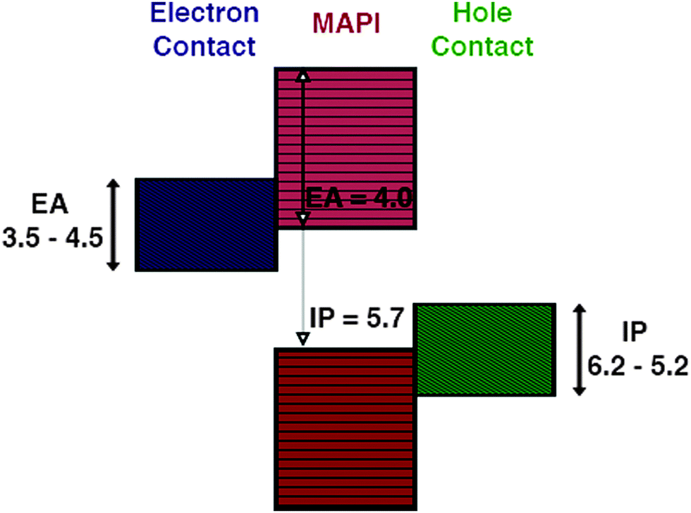 | ||
| Fig. 1 Electronic criteria for applicable contact layers for the CH3NH3PbI3 (MAPI) absorber layer. Contacts should have ionisation potentials (hole contact) and electron affinities (electron contact), commensurate with the valence and conduction bands of MAPI respectively. | ||
A selection of IP, EA, and Eg values from experiment and high-level theory, as well as some estimated by electronegativity arguments,33–76 for 175 binary and ternary and quaternary semiconductors was assembled for the purposes of this screening. The full list of screened values is available in the ESI.†
The nature of the contact will also depend on the conduction mechanism of the semiconductor (p- or n-type), which is determined by the doping limits77 and growth conditions. This level of prediction is beyond the scope of the screening procedure carried out in our study and the dopability of candidate materials may be assessed in further studies or by reference to the literature after our full screening is applied.
B. Epitaxy screening
We now turn our attention to the issue of the mechanical stability of the interfaces formed between the contact and CH3NH3PbI3. In cases where the crystal structure of the two materials forming the heterojunction are the same this is as simple as comparing the lattice parameters of both materials and assessing how closely they match. However, for materials with different crystal structures (as for the majority of heterojunctions of interest) the problem requires a little more thought. In this case Zur and McGill proposed a scheme78 whereby the two lattices are said to match if the interface translational symmetry could be compatible with the symmetry on both sides of the interface.This lattice matching is characterised by the precision of the match between cells and the area of the cells required to obtain that precision. For example one side of the interface (A) may have a lattice constant of 5.129 Å and the other a lattice (B) has a constant of 3.840 Å we then find that an expansion of 3 × A and 4 × B gives a lattice mismatch of around 0.2%. One could imagine that by applying such supercell expansions matching of almost any lattice pair is possible and therefore we set an upper boundary on the size to be considered, in our case we allow the lattice to expand up to five times in either surface vector.
The precision of the match gives a lower bound to the amount of strain required to form chemical bonds across the interface. For example if a precision of 1% is found for a pair of iso-structural materials, this means that the minimal distance that atoms on either side of the interface should shift to achieve bonding is ±0.5%. In general the strain induced by this shifting is alleviated by the formation of dislocations. Above a certain threshold of matching the strain can no longer be accommodated and incoherent interfaces, with extremely high defect concentrations, occur. As we wish to avoid such a situation, in our study we set a precision threshold of 5%.
The first problem when assessing the fit of two surfaces cleaved from a crystal is how to define the surface lattice. For example two similar lattices may be a rotation of one another. The lattices can be defined by their primitive vectors, however the choice of primitive vectors is not unique. Zur and McGill presented a reduction scheme which selects a set of primitive vectors for a surface in an almost unique way, selecting a set of primitive vectors independent of any rotations or reflections of the lattice.
The lattice matching technique applied here has previously been used to search for epitaxial heterointerfaces. It has been shown to robustly predict experimentally verified interface orientations of CdTe on GaAs,78 CdTe on sapphire,78 transition metal silicides on Si,79 PtNi3 on PtCo380 and Si on GaP.80
We begin by cleaving all of the low index surfaces of the materials identified in the electronic screening step, that is (h, k, l) h, k, l = 1 or 0, h + k + l > 0. We then apply the reduction scheme of Zur and McGill to obtain the primitive vectors (Fig. 2). Next we compare these primitive vectors with those of (110) and (100) surface of the pseudo-cubic CH3NH3PbI3 structure, using the supercell expansion and precision criteria outlined above. We note that at 300 K MAPI can exhibit a tetragonal distortion with c/a ≃ 1.01;81 however, the pseudo-cubic phase has also been reported for thin films at this temperature.82
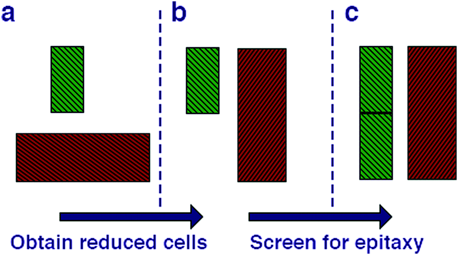 | ||
| Fig. 2 Methodology for screening for structural epitaxy. (a) Surface cells are defined based on all low index terminations. (b) The algorithm of Zur and McGill78 is applied to ensure that all surface cells are reduced to a reduced set of primitive translations. (c) Screening of supercell expansions of each material (up to a certain threshold) for lattice matching within a certain mismatch percentage. | ||
C. Atomic arrangement
Having identified the interface combinations which allow for a lattice mismatch within our cutoff criterion of 5% we assess how well chemical bonds will form across the interface. As Zur and McGill note in their original paper the mismatch criterion is secondary to the chemistry of the interface in determining the conditions optimal for growth, however the mismatch criterion offers a simple way to quantify a necessary (but not sufficient) condition for (semi-)coherent interface formation.To further assess the chemical viability of an interface we search for interfaces with the maximal overlap of atomic positions. We begin our procedure by defining the atom positions in the surface plane of two materials (see Fig. 3). In many cases for complex materials there is more than one surface termination possible for a given plane. We enumerate and consider all surfaces which have non-polar terminations (type-I or type-II in Tasker classification83); this enumeration is performed using the METADISE84 code.
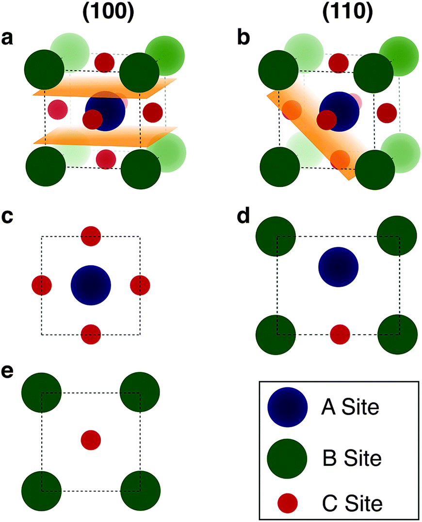 | ||
| Fig. 3 Illustration of the procedure to generate surface atom positions. (a and b) The (100) and (110) planes of the ideal cubic perovskite are cut along all identified non-polar surfaces, the orange sections indicate the plane of cleavage. For the (110) surface the removal of an oxygen ion from the surface layer is required to remove the polarity. (c–e) The positions of the under-coordinated atoms at the surfaces indicated by orange sections in (a and b) are projected into a plane for matching with other interfaces. | ||
Next we expand the lattices by the ratios determined in the previous screening step for epitaxy. In our case we are examining systems with different crystal structures, so we will not necessarily obtain complete overlap of lattice sites. Instead we define a cutoff radius (5% of the CH3NH3PbI3(110) u vector, or 0.3 Å), if we obtain overlap within that radius we count the sites as coincident (filled burgundy circles in Fig. 4(b)). We apply translations of the contacting surface with respect to the CH3NH3PbI3 surface, selecting the configuration with maximum overlap to calculate our atomic site overlap (ASO) ratio. The ASO ratio is defined as
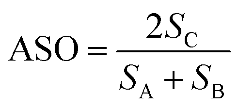 | (2) |
![[1 with combining macron]](https://www.rsc.org/images/entities/char_0031_0304.gif) 0) surface.
0) surface.
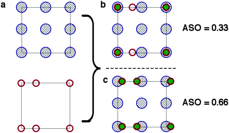 | ||
| Fig. 4 Conditions for the identification of atomic site overlap (ASO) of two surface cells (a). The atomic positions of the two cells are overlayed. (b) If the centres are within a threshold separation they are counted as coinciding (filled green circles). (c) The lattices are translated with respect to one another in order to maximise the ASO factor (eqn (2)). | ||
We note that we have taken no account of the nature of the atoms occupying the lattice sites, simply treating all points as equal. For a more rigorous assessment of the suitability of a combination of materials surfaces one could take into account the formal charges of the species at each site, such that positive and negative ions would compensate for one another. Furthermore, quantities such as ionic radii and chemical hardness/softness of the species occupying a site can give further insight into the propensity for two surfaces to form mechanically stable interfaces. In the context of this methodology, which is primarily designed to provide a swift and simple screening procedure for the identification of possible promising interface matches, however, we neglect the difference between sites. To test the validity of our approximations we have screened possible interfaces of GaN/ZnO, the procedure is outlined in detail in the supporting information, the combination of lattice and site screening correctly identifies the experimentally observed interfaces, filtering out less favourable combinations that have not been experimentally observed.
IV. Identified materials
The most suitable contact materials obtained after our screening procedure are listed in Table 1 along with information relating to their band offset (calculated from IP and EA) and the strain and lattice matching at the interface. For the band offsets (ϕx) a negative value indicates that the transfer of the carrier (electron or hole) from CH3NH3PbI3 to the contact material is energetically favoured based on IP or EA values, a positive value indicates a barrier. We find 16 materials with an ELS of ≥10. We note that all materials in our initial set, which have been reported as contact layers in the context of CH3NH3PbI3 are identified as successful candidate materials after screening, lending validity to the procedure.| Material | Surface | ΔVBM (eV) | ΔCBM (eV) | Multiplicity A | Multiplicity B | Strain (%) | ASO | ELS | |||
|---|---|---|---|---|---|---|---|---|---|---|---|
| u | v | u | v | u | v | ||||||
| MAPI | 110 | ||||||||||
| Ce2O3 | 110 | 0 | 1 | 4 | 1 | 3 | 1.8 | 2.4 | 0.3 | 10 | |
| Ce2S3 | 101 | 0.0 | 3 | 1 | 2 | 2 | 2.4 | 1.9 | 0.3 | 10 | |
| CoO | 110 | −0.4 | 3 | 3 | 2 | 2 | 1.5 | 1.8 | 0.3 | 8 | |
| Cu2O | 110 | 0.0 | 3 | 3 | 2 | 2 | 1.6 | 1.9 | 0.3 | 10 | |
| CuI | 001 | 0.1 | 1 | 3 | 1 | 2 | 3.8 | 2.3 | 0.3 | 8 | |
| CuI | 110 | 0.1 | 1 | 1 | 1 | 1 | 3.8 | 3.5 | 0.6 | 12 | |
| FeO | 100 | −0.3 | 3 | 2 | 2 | 1 | 2.6 | 0.3 | 0.3 | 11 | |
| FeO | 110 | −0.3 | 3 | 3 | 2 | 2 | 2.6 | 2.8 | 0.3 | 7 | |
| GaN | 100 | −0.1 | 2 | 5 | 1 | 3 | 1.3 | 2.7 | 0.6 | 18 | |
| GaN | 110 | −0.1 | 5 | 5 | 1 | 3 | 3.0 | 3.6 | 0.4 | 8 | |
| In2O3 | 110 | 0.3 | 3 | 3 | 5 | 5 | 3.6 | 3.4 | 0.1 | 2 | |
| LiNbO3 | 100 | 0.2 | 5 | 2 | 4 | 3 | 2.8 | 4.0 | 0.3 | 7 | |
| MnTiO3 | 100 | 0.0 | 5 | 3 | 4 | 5 | 1.9 | 3.6 | 0.3 | 8 | |
| NaNBO3 | 110 | 0.2 | 5 | 5 | 3 | 3 | 3.3 | 3.6 | 0.2 | 4 | |
| NiO | 110 | −0.4 | 3 | 3 | 2 | 2 | 0.4 | 0.2 | 0.3 | 18 | |
| Pr2S3 | 101 | 0.1 | 3 | 1 | 2 | 2 | 3.5 | 2.6 | 0.3 | 7 | |
| SiC | 110 | 0 | 5 | 5 | 3 | 3 | 0.2 | 0.0 | 0.5 | 45 | |
| Sm2S3 | 110 | 0.3 | 3 | 3 | 4 | 5 | 0.2 | 3.7 | 0.4 | 12 | |
| SnS2 | 100 | −0.2 | 5 | 3 | 3 | 2 | 3.8 | 0.7 | 0.3 | 9 | |
| SrTiO3 | 110 | −0.1 | 5 | 5 | 3 | 3 | 3.3 | 3.5 | 0.4 | 10 | |
| Tb2S3 | 110 | 0.3 | 3 | 4 | 5 | 5 | 0.0 | 2.3 | 0.3 | 11 | |
| TiO2 r | 011 | −0.2 | 4 | 5 | 3 | 3 | 2.6 | 2.5 | 0.3 | 8 | |
| ZnO | 100 | −0.2 | 2 | 5 | 1 | 3 | 3.2 | 2.2 | 0.6 | 14 | |
| ZnTe | 100 | −0.1 | 1 | 3 | 1 | 2 | 3.1 | 3.0 | 0.3 | 8 | |
| ZnTe | 110 | −0.1 | 1 | 1 | 1 | 1 | 3.1 | 2.9 | 0.4 | 11 | |
| ZnTiO3 c | 011 | −0.3 | 5 | 5 | 4 | 3 | 0.1 | 3.0 | 0.3 | 9 | |
| MAPI | 100 | ||||||||||
| Ce2S3 | 100 | 0.0 | 3 | 2 | 2 | 5 | 2.1 | 0.0 | 0.2 | 8 | |
| CoO | 100 | −0.4 | 3 | 3 | 2 | 2 | 1.9 | 1.5 | 0.3 | 8 | |
| Cu2O | 100 | 0.0 | 3 | 3 | 2 | 2 | 2.0 | 1.6 | 0.3 | 10 | |
| CuI | 100 | 0.1 | 1 | 1 | 1 | 1 | 3.4 | 3.8 | 0.8 | 17 | |
| CuI | 110 | 0.1 | 1 | 3 | 1 | 4 | 3.4 | 2.1 | 0.4 | 11 | |
| FeO | 100 | −0.3 | 3 | 3 | 2 | 2 | 2.9 | 2.6 | 0.3 | 7 | |
| FeO | 110 | −0.3 | 3 | 1 | 2 | 1 | 2.9 | 3.3 | 0.7 | 13 | |
| GaN | 100 | −0.1 | 2 | 5 | 1 | 4 | 1.7 | 3.0 | 0.6 | 17 | |
| In2O3 | 100 | −0.3 | 3 | 3 | 5 | 5 | 3.3 | 3.7 | 0.1 | 2 | |
| In2S3 | 100 | 0.0 | 4 | 1 | 5 | 5 | 2.9 | 2.7 | 0.1 | 4 | |
| NaNbO3 | 100 | 0.2 | 5 | 5 | 3 | 3 | 3.7 | 3.3 | 0.4 | 8 | |
| Nd2S3 | 110 | 0.3 | 3 | 2 | 4 | 5 | 1.1 | 1.4 | 0.2 | 7 | |
| NiO | 100 | −0.4 | 3 | 3 | 2 | 2 | 0.1 | 0.4 | 0.3 | 19 | |
| Pr2S3 | 100 | 0.1 | 3 | 2 | 2 | 5 | 3.1 | 0.8 | 0.2 | 6 | |
| SiC | 100 | 0.0 | 2 | 5 | 1 | 4 | 1.8 | 0.3 | 0.6 | 27 | |
| Sm2S3 | 110 | 0.3 | 3 | 2 | 4 | 5 | 0.1 | 2.4 | 0.2 | 7 | |
| SnO2 | 001 | 0.0 | 4 | 4 | 3 | 3 | 0.7 | 0.3 | 0.4 | 25 | |
| SrTiO3 | 100 | −0.1 | 5 | 5 | 3 | 3 | 3.6 | 3.3 | 0.4 | 10 | |
| Tb2S3 | 010 | 0.3 | 3 | 3 | 5 | 5 | 0.3 | 1.7 | 0.2 | 9 | |
| TiO2 a | 001 | −0.2 | 5 | 5 | 3 | 3 | 0.5 | 0.2 | 0.4 | 27 | |
| TiO2 a | 100 | −0.2 | 5 | 2 | 3 | 3 | 0.5 | 0.7 | 0.4 | 23 | |
| TiO2 a | 101 | −0.2 | 5 | 3 | 3 | 5 | 0.5 | 2.4 | 0.2 | 7 | |
| TiO2 r | 001 | −0.2 | 4 | 4 | 3 | 3 | 2.4 | 2.8 | 0.4 | 10 | |
| ZnO | 100 | −0.2 | 2 | 5 | 1 | 4 | 3.6 | 3.4 | 0.6 | 12 | |
| ZnTe | 100 | −0.1 | 1 | 1 | 1 | 1 | 2.7 | 3.1 | 0.5 | 13 | |
| ZnTe | 110 | −0.1 | 1 | 3 | 1 | 4 | 2.8 | 2.8 | 0.3 | 8 | |
A. Critical appraisal of existing contact layers
TiO2 is by far the most commonly applied electron contact material in perovskite solar cells, it has been reported as contact in both rutile and anatase structures. The phase of the material can have an effect on the band offset with respect to CH3NH3PbI3 as has been noted previously in the context of photocatalysis,85 however, given the spread in values reported for each phase and strong influence of surface orientation we have used one representative value for all phases of TiO2, more refined future studies could account for the influence of crystal structure on electron energies. In terms of mechanical stability the anatase(001) surface results in the best combination of low mismatch and the high ASO ratio of all of the possible TiO2 faces suggesting that it should be the most stable. Indeed, we note that rutile TiO2 generally has a significantly greater strain than the anatase layers, which can result in the formation of greater density of defects at the rutile TiO2/CH3NH3PbI3 interface. The highly matched surface of (001) anatase TiO2 (our best identified surface for mechanical matching) explains the experimental observation that CH3NH3PbI3 grown on (001) oriented nanoplatlets of TiO2 shows better crystallinity and larger grain sizes than those grown on a standard mesoporous substrate.86 This suggests a route for synthesis of better quality perovskite layers, based on optimisation of site matching and minimisation of lattice strain. We also note that a sensitivity analysis of the effect of the band offset on the calculated ELS, across the experimentally reported range of values (taken from ref. 87) shows that the values for the favoured interfaces (anatase 001 and 100) range from 15–27, meaning that they are still predicted to be some of the most suitable contacts.ZnO has also been reported as an electron extraction contact,18,19 allowing for lower temperature synthesis of working devices. Indeed the performance of devices containing TiO2, ZnO and CdS electron extraction layers has been reported.19 The authors report that TiO2 and ZnO cells show comparable performance, but the CdS based cells show much diminished efficiencies. Based on the alignment of energy levels there is little difference between the three materials for efficient electron extraction, indeed all three remain after the first step in our screening. However, based on interface epitaxy CdS was ruled out in our screening as it could not meet the criteria for mechanical strain. The strain at the CdS/absorber interface could lead to deformation of the band energies or the formation of defects at the interface, both of which would contribute to the diminished performance reported. The mismatch factor for ZnO, however is not as favourable as the best TiO2 interfaces, this, coupled with the chemistry of the interface, as recently suggested by De Angelis and co workers23 may also have a bearing on the stability.
SnO2 does not, in general, meet the criteria for good band alignment with CH3NH3PbI3; however, in this material the effect of surface termination on the EA and IP can be very pronounced.87 In this case the initial screening suggests that SnO2 does not form a good electronic contact. For our analysis we have included the (001) orientation, which has an IP calculated to be 7.47 eV and an EA of 4.04 eV, this is almost perfectly aligned to CH3NH3PbI3 for electron extraction without energy loss. In addition the (001) orientation shows minimal strain with CH3NH3PbI3 as well as good atomic site overlap. These findings suggest that growth of CH3NH3PbI3 on (001) oriented SnO2 could lead to excellent quality devices with clean interfaces, however, we would expect architectures based on SnO2 to be more sensitive to the growth conditions than those based on TiO2.
CuI has recently been reported as a hole extraction material to replace the usual organic material,21 with excellent photocurrent stability and high carrier mobility. The devices did display higher interface recombination than Spiro-OMeTAD based devices, which can be related to the barrier in band energy between the perovskite and CuI I. However, the lattice matching and ASO both suggest mechanically stable interface formation; experimentally the cells were found to be stable without encapsulation for 54 days.21 The screening methodology outlined here can be applied in the search for hole extraction materials with better band offsets and equivalent mechanical stability.
B. New routes to contacting CH3NH3PbI3
The materials discussed thus far have been previously considered for application in CH3NH3PbI3 solar cells. Although the discussion of preferred orientations and morphologies in the context of degrees of lattice and electronic matching provides clear routes for optimisation of devices. In addition, however, our screening has suggested a number of alternative materials which have (to our knowledge) not hitherto been applied in the context of CH3NH3PbI3 solar cells.The new material that displays the most obvious potential for contacting CH3NH3PbI3 on the basis of the ELS figure of merit is SiC. SiC can act as a p- or n-type semiconductor depending on doping, it crystalises as many different polytypes. Due to this polytypism the ELS figure of merit is sensitive to growth conditions. The common 2H hexagonal polymorph shows excellent interfacial matching with pseudo-cubic CH3NH3PbI3. Details of the IP and EA would also be expected to be sensitive to the crystal structure88 and this system merits further investigation for potential application as a contacting layer in halide perovskite cells. The SiC band gap of 2.36 eV means that it is not totally transparent, therefore in terms of device design a back layer of SiC is preferable to a front contact.
Transition metal oxides (TMOs) are commonly applied in organic photovoltaics (OPV) as hole transport layers, so a direct application in the same context for CH3NH3PbI3 may seem reasonable. Of the TMOs used in OPV devices NiO is by far the most promising from our analysis. It has a reasonable match of IP with CH3NH3PbI3 and the matching of the (110) and (100) surfaces of the two materials is extremely good, in both cases the matching with NiO is as good as the matching with TiO2 and NiO has a high ELS value, we note that there have been initial reports of the successful application of NiO in halide perovskite solar cells.89,90 FeO also has promising ELS values for certain orientations, the (100) surface matches to CH3NH3PbI3(110) and vice versa. CoO has a promising band alignment with CH3NH3PbI3, but poor site matching at the interface means that the ELS value is relatively low. Other TMOs such as MoO3,WO3 and V2O5, which are commonly applied in organic photovoltaics, have too large values of IP to align well with CH3NH3PbI3.
GaN shows potential as an electron extraction layer suggested from our screening. It has excellent band alignment with CH3NH3PbI3 and the (100) surface matches well with the (110) surface of CH3NH3PbI3. It has ELS values similar to CuI and superior to ZnO. It also has the obvious advantage that it is well known as an n-type semiconductor91 and can be controllably doped with Si or O.
Cu2O has excellent band alignment with CH3NH3PbI3, suggesting potentially barrier-less contact. The lattice mismatch is reasonable and the ELS of 10 means that it is potentially useful as a contact material. Cu2O is also well known to have p-type conductivity controllable by the synthesis conditions92 and is earth-abundant making it highly suited in the context of photovoltaic energy generation.
ZnTe, although less earth-abundant than Cu2O, also shows promising interface mismatch and band alignment to CH3NH3PbI3. It is also a p-type semiconductor and is commonly applied in a similar role in the context of CdTe solar cells, where it is used as a hole extraction layer.
Ce2O3,Ce2S3 and Sm2S3 were all identified as having ELS values of 10 or greater; however, for reasons of resource scarcity or supply risk they are not considered any further. Ce is exceedingly rare with a very low crustal abundance, whilst Pr and Sm are both considered critical materials and have a high supply risk. The flexibility of our current screening procedure means that concerns of supply and abundance could easily be facilitated in the figure of merit, in a similar way to a recent study which screened earth abundant thermoelectrics.93
Oxide perovskites have been considered as electron extracting layers (in the case of SrTiO394). Sharing the same crystal structure as CH3NH3PbI3 means that they can have potentially superior matching of atomic sites at the interface. The perovskites studied here with cubic structures (SrTiO3 and NaNbO3) have a very good match in terms of EA for electron extraction from CH3NH3PbI3. In terms of interface mismatch they are a reasonable match for CH3NH3PbI3, with as good matching as, for example, commonly applied ZnO. Also, given the wide range of chemical formulas which conform to the Goldschmidt tolerance factor for cubic perovskites, it is possible to imagine designing of better matched alternatives. ZnTiO3 and MnTiO3 both crystallise in the rhombohedrally distorted perovskite structure; the R![[3 with combining macron]](https://www.rsc.org/images/entities/char_0033_0304.gif) space group (number 148), nonetheless they have interface matching (with the (110) CH3NH3PbI3 surface) to the cubic species mentioned. In addition they have promising band alignment, with the caveat that these values are not from experiment or high level theory, but were estimated on the basis of Mulliken electronegativity of the compounds.
space group (number 148), nonetheless they have interface matching (with the (110) CH3NH3PbI3 surface) to the cubic species mentioned. In addition they have promising band alignment, with the caveat that these values are not from experiment or high level theory, but were estimated on the basis of Mulliken electronegativity of the compounds.
C. Designing new materials for contacting
The above study has considered only set of well known and characterised binary and ternary semiconductors. High-throughput computation offers an increasingly attractive route for the design and discovery of materials and resources such as the Materials Project95,96 mean that increasing amounts of the required data are available. The extension of the methodology outlined above to ternary and quaternary semiconductors can easily be imagined through the application of data mining approaches.93,97 The problem, from the perspective of the experimental data required is the lack of good data for IPs and EAs. These quantities are accessible by computation, but generally the cost of calculation is greater than the cost of calculation of lattice parameters and band gaps. Therefore we could easily apply an inversion of the above screening methodology: screening for mechanical stability followed by calculation of IPs and EAs for promising materials, possibly applying inexpensive schemes before a full first-principles treatment. Additionally approximate methods for the estimation of IPs and EAs, such as, model solid theory,98 universal hydrogen alignment,99 Mulliken electronegativity100 or solid state energy101 can be used. As with all data searching techniques the application of a useful figure of merit is critical, the ELS number described herein is a useful first approximation, with the application of higher levels of theory more subtle measures such as the spectroscopically limited SLME method of Yu and Zunger102 could be applied. One need not be limited by application of a single material, as we have previously demonstrated the ability to tune electronic alignments by the application of ultra-thin inter-layers.103 The application of materials design techniques is limited only by imagination.V. Conclusions
We have presented a simple methodology to screen for electronically aligned, mechanically robust interfaces, which can be applied to search for materials combinations in the context of any semiconductor application. The methodology requires only basic properties of the candidate materials, namely lattice constants, crystal structure, ionisation potential and electron affinity.We applied this methodology to screen 175 common semiconductor materials for application as contacts (both hole and electron extracting) in hybrid perovskite solar cells. From our initial set 16 materials were identified as good candidates for contacting – including all of the materials in our test set which have been successfully applied in the hybrid perovskite devices previously. In addition we suggest possible new architectures, which could lead to improved performance or enhanced device stability.Those identified materials which were not ruled out due to supply concerns along with their ELS values are presented in an energy-band-alignment diagram in Fig. 5.
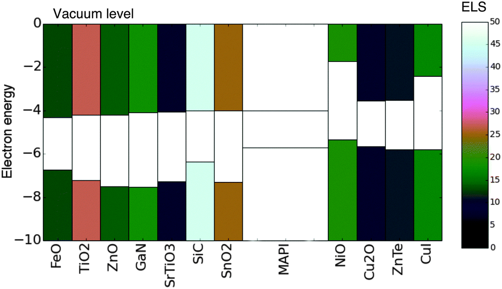 | ||
| Fig. 5 Materials identified as having a favourable ELS value. The valence and conduction bands of each material are shaded according to the ELS value (colourbar to the right). Electron extraction layers are placed to the left of CH3NH3PbI3 (MAPI) and hole extraction layers are placed to the right. All electron energies are in (eV). Note several materials with ELS ≥10 are not included due to scarcity of constituent species. All values are presented in Table 1. | ||
It is important to emphasise that the ELS method presented identifies candidate contacting materials that meet a number of necessary conditions, it does not guarantee that a material will form a good contact. Other factors should also be assessed in order to discriminate amongst the promising materials. Importantly conductivity should be considered, this is a combination of carrier mobility and concentration. Both of these values are potentially accessible from first principles calculations and could be appended as a further computational screening step. Processability of a material is also an important practical concern, however this is difficult to predict from calculations and is best determined by the expert practitioner. Nonetheless, the application of our method significantly focuses the space within which these more detailed assessments must be performed.
The study presented was limited to a set of well known and studied semiconductor materials. However, with the advent of computational high-throughput screening of materials such a study can easily be extended to the search for new materials or novel combinations of old materials. The simplicity of the concepts and ease of computation mean that this methodology can be easily applied by researchers in the field of semiconductors with access to a reasonable desktop computer and a basic knowledge of modern computer scripting languages. As such we hope that this tool may be of use to experimental and modelling groups alike in the continuing search for functional materials combinations.
Acknowledgements
K. T. B. acknowledges support by a JSPS Postdoctoral Fellowship for Overseas Researchers. Y. K. and F. O. are supported by the MEXT Elements Strategy Initiative to Form Core Research Center. F. O. acknowledges support by Grants-in-Aid for Scientific Research (B) and Scientific Research on Innovative Areas (Grant No. 15H04125 and 25106005) from JSPS, and Support Program for Starting Up Innovation Hub from JST. A. W. acknowledges support from the Royal Society for a University Research Fellowship and K. T. B. is funded by EPSRC (EP/M009580/1 and EP/J017361/1).References
- A. Kojima, K. Teshima, Y. Shirai and T. Miyasaka, J. Am. Chem. Soc., 2009, 131, 6050 CrossRef CAS PubMed.
- M. M. Lee, J. Teuscher, T. Miyasaka, T. N. Murakami and H. J. Snaith, Science, 2012, 338, 643 CrossRef CAS PubMed.
- N. J. Jeon, J. Lee, J. H. Noh, M. K. Nazeeruddin, M. Grätzel and S. I. Seok, J. Am. Chem. Soc., 2013, 135, 19087 CrossRef CAS PubMed.
- M. Grätzel, Nat. Mater., 2014, 13, 838 CrossRef PubMed.
- M. A. Green, K. Emery, Y. Hishikawa, W. Warta and E. D. Dunlop, Prog. Photovoltaics, 2015, 23, 1 Search PubMed.
- T. Leijtens, G. E. Eperon, N. K. Noel, S. N. Habisreutinger, A. Petrozza and H. J. Snaith, Adv. Energy Mater., 2015, 5, 1500963 Search PubMed.
- D. Shi, V. Adinolfi, R. Comin, M. Yuan, E. Alarousu, A. Buin, Y. Chen, S. Hoogland, A. Rothenberger, K. Katsiev, Y. Losovyj, X. Zhang, P. A. Dowben, O. F. Mohammed, E. H. Sargent and O. M. Bakr, Science, 2015, 347, 519 CrossRef CAS PubMed.
- H. Zhou, Q. Chen, G. Li, S. Luo, T.-b. Song, H.-S. Duan, Z. Hong, J. You, Y. Liu and Y. Yang, Science, 2014, 345, 542 CrossRef CAS PubMed.
- J. Shi, X. Xu, D. Li and Q. Meng, Small, 2015, 11, 2472 CrossRef CAS PubMed.
- K. T. Butler, P. E. Vullum, A. M. Muggerud, E. Cabrera and J. H. Harding, Phys. Rev. B: Condens. Matter Mater. Phys., 2011, 83, 235307 CrossRef.
- K. T. Butler and J. H. Harding, Phys. Rev. B: Condens. Matter Mater. Phys., 2012, 86, 245319 CrossRef.
- Y. Hinuma, F. Oba, Y. Kumagai and I. Tanaka, Phys. Rev. B: Condens. Matter Mater. Phys., 2013, 88, 035305 CrossRef.
- P. Schulz, E. Edri, S. Kirmayer, G. Hodes, D. Cahen and A. Kahn, Energy Environ. Sci., 2014, 7, 1377 CAS.
- V. Gonzalez-Pedro, E. J. Juarez-Perez, W.-S. Arsyad, E. M. Barea, F. Fabregat-Santiago, I. Mora-Sero and J. Bisquert, Nano Lett., 2014, 14, 888 CrossRef CAS PubMed.
- N.-G. Park, J. Phys. Chem. Lett., 2013, 4, 2423 CrossRef CAS.
- A. Mei, X. Li, L. Liu, Z. Ku, T. Liu, Y. Rong, M. Xu, M. Hu, J. Chen, Y. Yang, M. Grätzel and H. Han, Science, 2014, 345, 295 CrossRef CAS PubMed.
- D. Liu and T. L. Kelly, Nat. Photonics, 2013, 8, 133 CrossRef.
- M. H. Kumar, N. Yantara, S. Dharani, M. Graetzel, S. Mhaisalkar, P. P. Boix and N. Mathews, Chem. Commun., 2013, 49, 11089 RSC.
- E. J. Juarez-Perez, M. Wußler, F. Fabregat-Santiago, K. Lakus-Wollny, E. Mankel, T. Mayer, W. Jaegermann and I. Mora-Sero, J. Phys. Chem. Lett., 2014, 5, 680 CrossRef CAS PubMed.
- D.-Y. Son, J.-H. Im, H.-S. Kim and N.-G. Park, J. Phys. Chem. C, 2014, 118, 16567 CAS.
- J. A. Christians, R. C. M. Fung and P. V. Kamat, J. Am. Chem. Soc., 2014, 136, 758 CrossRef CAS PubMed.
- A. Murray, J. M. Frost, C. Hendon, C. D. Molloy, D. Carbery and A. Walsh, Chem. Commun., 2015, 51, 8935 RSC.
- V. Roiati, E. Mosconi, A. Listorti, S. Colella, G. Gigli and F. De Angelis, Nano Lett., 2014, 14, 2168 CrossRef CAS PubMed.
- K. Butler, J. M. Frost and A. Walsh, Energy Environ. Sci., 2015, 8, 838 CAS.
- C. Wood, H. Li, P. Winget and J.-L. Brédas, J. Phys. Chem. C, 2012, 116, 19125 CAS.
- J. Yang, B. D. Siempelkamp, E. Mosconi, F. De Angelis and T. L. Kelly, Chem. Mater., 2015, 27, 4229 CrossRef CAS.
- M. W. Lamers, K. T. Butler, J. H. Harding and A. Weeber, Sol. Energy Mater. Sol. Cells, 2012, 106, 17 CrossRef CAS.
- K. T. Butler, C. H. Hendon and A. Walsh, ACS Appl. Mater. Interfaces, 2014, 6, 22044 CAS.
- R. L. Anderson, IBM J. Res. Dev., 1960, 4, 280 CrossRef.
- A. Niemegeers, M. Burgelman and A. De Vos, Appl. Phys. Lett., 1995, 67, 843 CrossRef CAS.
- F. Brivio, K. T. Butler, A. Walsh and M. van Schilfgaarde, Phys. Rev. B: Condens. Matter Mater. Phys., 2014, 89, 155204 CrossRef.
- K. Butler, J. M. Frost and A. Walsh, Mater. Horiz., 2015, 228 RSC.
- G. D. Wilk, R. M. Wallace and J. M. Anthony, J. Appl. Phys., 2001, 89, 5243 CrossRef CAS.
- S. R. Desai, H. Wu, C. M. Rohlfing and L.-S. Wang, J. Chem. Phys., 1997, 106, 1309 CrossRef CAS.
- A. Grüneis, G. Kresse, Y. Hinuma and F. Oba, Phys. Rev. Lett., 2014, 112, 096401 CrossRef PubMed.
- M. E. Levinshtein, S. L. Rumyantsev and M. S. Shur, Properties of Advanced Semiconductor Materials: GaN, AIN, InN, BN, SiC, SiGe, John Wiley & Sons, 2001, p. 194 Search PubMed.
- H. Teisseyre, P. Perlin, T. Suski, I. Grzegory, S. Porowski, J. Jun, A. Pietraszko and T. D. Moustakas, J. Appl. Phys., 1994, 76, 2429 CrossRef CAS.
- S. Fonash, Solar Cell Device Physics, Elsevier, 2012, p. 352 Search PubMed.
- S. Adachi, Handbook on Physical Properties of Semiconductors, Springer Science & Business Media, 2004, vol. 2 Search PubMed.
- Y. Kaneko and T. Koda, J. Cryst. Growth, 1988, 86, 72 CrossRef CAS.
- K. Y. Tsou and E. B. Hensley, J. Appl. Phys., 1974, 45, 47 CrossRef.
- F. E. Martin and E. B. Hensley, Phys. Rev., 1967, 163, 219 CrossRef CAS.
- Y. Matsumoto, J. Solid State Chem., 1996, 126, 227 CrossRef CAS.
- O. Madelung, Semiconductors: Data Handbook, Springer Science & Business Media, 2012, p. 691 Search PubMed.
- B. Quiniou, W. Schwarz, Z. Wu, R. M. Osgood, Q. Yang and J. M. Phillips, Appl. Phys. Lett., 1992, 60, 183 CrossRef CAS.
- W. Lehmann, J. Electrochem. Soc., 1970, 117, 1389 CrossRef CAS.
- W. H. Strehlow and E. L. Cook, J. Phys. Chem. Ref. Data, 1973, 2, 163 CrossRef CAS.
- K. T. Butler, Phys. Status Solidi A, 2015, 212, 1461 CrossRef CAS.
- R. T. Poole, J. G. Jenkin, J. Liesegang and R. C. G. Leckey, Phys. Rev. B: Condens. Matter Mater. Phys., 1975, 11, 5179 CrossRef CAS.
- J. Deuermeier, J. Gassmann, J. Brotz and A. Klein, J. Appl. Phys., 2011, 109, 113704 CrossRef.
- T. Thomas, X. Guo, M. Chandrashekhar, C. B. Poitras, W. Shaff, M. Dreibelbis, J. Reiherzer, K. Li, F. J. DiSalvo, M. Lipson and M. Spencer, J. Cryst. Growth, 2009, 311, 4402 CrossRef CAS.
- K. J. Reynolds, J. A. Barker, N. C. Greenham, R. H. Friend and G. L. Frey, J. Appl. Phys., 2002, 92, 7556 CrossRef CAS.
- L.-S. Wang, H. Wu, S. R. Desai, J. Fan and S. D. Colson, J. Phys. Chem., 1996, 100, 8697 CrossRef CAS.
- B. D. Pelatt, R. Ravichandran, J. F. Wager and D. A. Keszler, J. Am. Chem. Soc., 2011, 133, 16852 CrossRef CAS PubMed.
- S. Monaghan, P. Hurley, K. Cherkaoui, M. Negara and A. Schenk, Solid-State Electron., 2009, 53, 438 CrossRef CAS.
- A. Walsh and C. R. A. Catlow, J. Mater. Chem., 2010, 20, 10438 RSC.
- Q. Guo and A. Yoshida, J. Appl. Phys., 1994, 33, 2453 CrossRef CAS.
- S. X. Li, K. M. Yu, J. Wu, R. E. Jones, W. Walukiewicz, J. W. Ager, W. Shan, E. E. Haller, H. Lu and W. J. Schaff, Phys. Rev. B: Condens. Matter Mater. Phys., 2005, 71, 161201 CrossRef.
- L. I. Berger, Semiconductor Materials, CRC Press, 1996, p. 496 Search PubMed.
- P. W. Peacock and J. Robertson, Appl. Phys. Lett., 2003, 83, 2025 CrossRef CAS.
- R. Juryska, Phys. Status Solidi B, 1975, 72, K161 CrossRef CAS.
- A. Galtayries, S. Wisniewski and J. Grimblot, J. Electron Spectrosc. Relat. Phenom., 1997, 87, 31 CrossRef CAS.
- J. He, H. Lindström, A. Hagfeldt and S.-E. Lindquist, Sol. Energy Mater. Sol. Cells, 2000, 62, 265 CrossRef CAS.
- R. A. Knapp, Phys. Rev., 1963, 132, 1891 CrossRef CAS.
- J. Robertson, J. Vac. Sci. Technol., B: Microelectron. Nanometer Struct.–Process., Meas., Phenom., 2000, 18, 1785 CrossRef CAS.
- M. Bozack, Phys. Status Solidi B, 1997, 202, 549 CrossRef CAS.
- S. M. Sze, Semiconductor Devices: Physics and Technology, 2008 Search PubMed.
- R. H. Williams, R. B. Murray, D. W. Govan, J. M. Thomas and E. L. Evans, J. Phys. C: Solid State Phys., 1973, 6, 3631 CrossRef CAS.
- J. M. Fitz-Gerald, J. Hoekstra, P. D. Rack and J. D. Fowlkes, Appl. Phys. Lett., 2003, 82, 3466 CrossRef CAS.
- B. C.-M. Lai, J. Electrochem. Soc., 1999, 146, 266 CrossRef CAS.
- S. F. Cogan, N. M. Nguyen, S. J. Perrotti and R. D. Rauh, J. Appl. Phys., 1989, 66, 1333 CrossRef CAS.
- H.-J. Zhai and L.-S. Wang, J. Chem. Phys., 2002, 117, 7882 CrossRef CAS.
- C. W. Walter, C. F. Hertzler, P. Devynck, G. P. Smith and J. R. Peterson, J. Chem. Phys., 1991, 95, 824 CrossRef CAS.
- R. A. Powell, W. E. Spicer and J. C. McMenamin, Phys. Rev. B: Condens. Matter Mater. Phys., 1972, 6, 3056 CrossRef CAS.
- L. Ley, R. A. Pollak, F. R. McFeely, S. P. Kowalczyk and D. A. Shirley, Phys. Rev. B: Condens. Matter Mater. Phys., 1974, 9, 600 CrossRef CAS.
- Y. Xu and M. A. Schoonen, Am. Mineral., 2000, 85, 543 CrossRef CAS.
- A. Walsh, J. Buckeridge, C. R. A. Catlow, A. J. Jackson, T. W. Keal, M. Miskufova, P. Sherwood, S. A. Shevlin, M. B. Watkins, S. M. Woodley and A. A. Sokol, Chem. Mater., 2013, 25, 2924 CrossRef CAS.
- A. Zur and T. C. McGill, J. Appl. Phys., 1984, 55, 378 CrossRef CAS.
- A. Zur, T. C. McGill and M. Nicolet, J. Appl. Phys., 1985, 57, 600 CrossRef CAS.
- A.-M. Raclariu, S. Deshpande, J. Bruggemann, W. Zhuge, T. Yu, C. Ratsch and S. Shankar, Comput. Mater. Sci., 2015, 108(part A), 88 CrossRef CAS.
- M. T. Weller, O. J. Weber, P. F. Henry, A. M. Di Pumpo and T. C. Hansen, Chem. Commun., 2015, 51, 4180 RSC.
- M. Xiao, F. Huang, W. Huang, Y. Dkhissi, Y. Zhu, J. Etheridge, A. Gray-Weale, U. Bach, Y.-B. Cheng and L. Spiccia, Angew. Chem., 2014, 126, 10056 CrossRef.
- P. W. Tasker, J. Phys. C: Solid State Phys., 1979, 12, 4977 CrossRef CAS.
- G. W. Watson, E. T. Kelsey, N. H. de Leeuw, D. J. Harris and S. C. Parker, J. Chem. Soc., Faraday Trans., 1996, 92, 433 RSC.
- D. O. Scanlon, C. W. Dunnill, J. Buckeridge, S. A. Shevlin, A. J. Logsdail, S. M. Woodley, C. R. A. Catlow, M. J. Powell, R. G. Palgrave, I. P. Parkin, G. W. Watson, T. W. Keal, P. Sherwood, A. Walsh and A. A. Sokol, Nat. Mater., 2013, 12, 798 CrossRef CAS PubMed.
- M. I. Dar, F. J. Ramos, Z. Xue, B. Liu, S. Ahmad, S. A. Shivashankar, M. K. Nazeeruddin and M. Grätzel, Chem. Mater., 2014, 26, 4675 CrossRef CAS.
- V. Stevanović, S. Lany, D. S. Ginley, W. Tumas and A. Zunger, Phys. Chem. Chem. Phys., 2014, 16, 3706 RSC.
- J. Buckeridge, K. T. Butler, C. R. A. Catlow, A. J. Logsdail, D. O. Scanlon, S. A. Shevlin, S. M. Woodley, A. A. Sokol and A. Walsh, Chem. Mater., 2015, 27, 3844 CrossRef CAS.
- J. H. Park, J. Seo, S. Park, S. S. Shin, Y. C. Kim, N. J. Jeon, H.-W. Shin, T. K. Ahn, J. H. Noh, S. C. Yoon, C. S. Hwang and S. I. Seok, Adv. Mater., 2015, 27, 4013 CrossRef CAS PubMed.
- L. Hu, J. Peng, W. Wang, Z. Xia, J. Yuan, J. Lu, X. Huang, W. Ma, H. Song, W. Chen, Y.-B. Cheng and J. Tang, ACS Photonics, 2014, 1, 547 CrossRef CAS.
- J. Buckeridge, C. Catlow, D. Scanlon, T. Keal, P. Sherwood, M. Miskufova, A. Walsh, S. Woodley and A. Sokol, Phys. Rev. Lett., 2015, 114, 016405 CrossRef CAS PubMed.
- L. Xiong, S. Huang, X. Yang, M. Qiu, Z. Chen and Y. Yu, Electrochim. Acta, 2011, 56, 2735 CrossRef CAS.
- M. W. Gaultois, T. D. Sparks, C. K. H. Borg, R. Seshadri, W. D. Bonificio and D. R. Clarke, Chem. Mater., 2013, 25, 2911 CrossRef CAS.
- A. Bera, K. Wu, A. Sheikh, E. Alarousu, O. F. Mohammed and T. Wu, J. Phys. Chem. C, 2014, 118, 28494 CAS.
- A. Jain, S. P. Ong, G. Hautier, W. Chen, W. D. Richards, S. Dacek, S. Cholia, D. Gunter, D. Skinner, G. Ceder and K. a. Persson, APL Mater., 2013, 1, 011002 CrossRef.
- G. Hautier, A. Miglio, G. Ceder, G.-M. Rignanese and X. Gonze, Nat. Commun., 2013, 4, 2292 Search PubMed.
- B. Meredig and C. Wolverton, Chem. Mater., 2014, 1985 CrossRef CAS.
- C. G. Van de Walle, Phys. Rev. B: Condens. Matter Mater. Phys., 1989, 39, 1871 CrossRef CAS.
- C. G. Van de Walle and J. Neugebauer, Nature, 2003, 423, 626 CrossRef CAS PubMed.
- I. E. Castelli, D. D. Landis, K. S. Thygesen, S. r. Dahl, I. Chorkendorff, T. F. Jaramillo and K. W. Jacobsen, Energy Environ. Sci., 2012, 5, 9034 CAS.
- B. D. Pelatt, R. S. Kokenyesi, R. Ravichandran, C. B. Pereira, J. F. Wager and D. A. Keszler, J. Solid State Chem., 2015, 231, 138 CrossRef CAS.
- L. Yu and A. Zunger, Phys. Rev. Lett., 2012, 108, 068701 CrossRef PubMed.
- K. T. Butler, J. Buckeridge, C. R. A. Catlow and A. Walsh, Phys. Rev. B: Condens. Matter Mater. Phys., 2014, 89, 115320 CrossRef.
Footnote |
| † Electronic supplementary information (ESI) available. See DOI: 10.1039/c5tc04091d |
| This journal is © The Royal Society of Chemistry 2016 |