
 Open Access Article
 This Open Access Article is licensed under a
 Creative Commons Attribution 3.0 Unported Licence
Band gap and work function tailoring of SnO2 for improved transparent conducting ability in photovoltaics
Alex M.
Ganose
*ab and
David O.
Scanlon
*ab
aDepartment of Chemistry, Kathleen Lonsdale Materials Chemistry, University College London, 20 Gordon Street, London WC1H 0AJ, UK. E-mail: alex.ganose.10@ucl.ac.uk; d.scanlon@ucl.ac.uk
bDiamond Light Source Ltd., Diamond House, Harwell Science and Innovation Campus, Didcot, Oxfordshire OX11 0DE, UK
First published on 14th January 2016
Abstract
Transparent conducting oxides (TCOs) are an essential component in modern optoelectronic devices, such as solar panels and touch screens. Their ability to combine transparency and conductivity, two properties that are normally mutually exclusive, have made them the subject of intense research over the last 50 years. SnO2, doped with F or Sb, is a widely used and relatively inexpensive transparent conducting material, however, its electronic structure leaves scope for improving its properties for use in many TCO applications, especially in solar cell devices. Here we show using density functional theory that incorporation of Pb into SnO2 reduces the band gap through lowering of the conduction band minimum, thereby increasing the electron affinity. The electron effective mass at the conduction band minimum decreases alongside the band gap, indicating improved charge carrier mobilities. Furthermore, the calculated optical absorption properties show the alloys retain their transparency in the visible spectrum. Our results suggest that alloying of PbO2 with SnO2 will enable improved electronic properties, including a highly tuneable workfunction, which will open up the material for other applications, such as hole injection layers in organic photovoltaics.
Introduction
Transparent conducting oxides (TCOs) are a class of materials that simultaneously possess the conflicting properties of optical transparency and conductivity. First documented over half a century ago,1 TCOs are now an essential component in modern optoelectronic devices, including flat panel displays, touch-screen sensors and solar cells.2–5 The industry standard n-type TCO is Sn-doped In2O3 (In2O3:Sn or ITO), which possesses excellent optical and electronic properties, with carrier densities exceeding 1021 cm−3, resistivities below 10−5 Ω cm and high optical transparency in the visible spectrum.6 However, the low abundance of indium in the earth's crust together with massive demand for ITO has lead to increasing concerns over indium supply.7,8 As such, the price of indium has fluctuated wildly in recent years and there are concerted efforts to eliminate its use in TCOs.9,10 Alternative materials such as ZnO:Al (AZO), SnO2:Sb (ATO), and SnO2:F (FTO) have been employed in a range of devices but have so far been unable to replicate the high performance seen in ITO.11There are several properties necessary for an n-type TCO to achieve optimal performance. The optical band gap, Eoptg, must be greater than 3.1 eV to provide transparency in the visible spectrum. Additionally, conductivity is dependent on the ability of the material to form a degenerate semiconductor upon donor doping, termed the dopability. In excellent n-type TCOs, donors will donate electrons directly into the conduction band (CB), leading to filled states at the conduction band minimum (CBM) and Moss–Burstein widening of the optical band gap.12–14 The dopability is largely controlled by the position of the CBM relative to the vacuum level, i.e. the electron affinity (EA).15–18 A large EA indicates that it is easier to get charge carriers into the system, effectively increasing carrier concentrations. To guarantee transparency after doping, a large separation from the first to the second conduction band (CBM to CBM + 1) is necessary to prevent interband excitation of electrons. Finally, a highly disperse CB ensures a small carrier effective mass at the CBM. This generally arises from having a CB composed of metal-s-like orbitals allowing for high carrier mobilities.19
The TCO deposited in the largest quantity, with regard to area, is F or Sb doped SnO2, for use in a variety of applications such as low-emissivity windows in buildings, electrochromic mirrors and defrosting windows in supermarkets.20 Undoped SnO2 is itself a prototypical TCO, with a large fundamental band gap of ∼3.6 eV,21 up to 97% transparency in the visible spectrum and carrier densities approaching 1021 cm−3.22 Importantly, as Sn is earth-abundant (∼30–40 times more abundant than In in the Earth's crust23), the raw materials needed for SnO2 are less expensive than for ITO.24 Manufacturing is also simplified due to the availability of chemical deposition methods, such as spray pyrolysis and atmospheric pressure chemical vapour deposition.25–28 Similar to other TCO materials, a debate exists as to whether intrinsic oxygen vacancies (VO) and tin interstitials (Sni) play a role in conduction.29,30 The most recent studies, however, have indicated that they are deep donors or have restrictively high formation energies.31,32 Instead, hydrogen acting as an unintentional donor (Hi or HO) has been identified both theoretically,31,33 and experimentally34,35 as a suitable defect to explain the conductivity seen in SnO2. Regardless, due to the propensity for native defects, hydrogen interstitials, and surface states to all be donor-like, King and Veal have argued that the charge neutrality level in n-type TCOs is likely to be above the CBM.36 Thus, donor defect states remain energetically favourable even when the Fermi level appears inside the conduction band. In SnO2, due to the large gap between the Fermi level and the energy level of the first unoccupied states, any such defects do not cause vertical optical transitions in the visible range, enabling high carrier concentrations with little effect on transparency.29
Comparison of the properties of In2O3 and SnO2 reveals many similarities: both are direct wide band gap semiconductors, have a CBM + 1 greater than 3.1 eV above the CBM, and have highly dispersed conduction bands.39 The EA of In2O3, however, is significantly larger than that of SnO2 and, in fact, of all other TCOs (Fig. 1).40 With the fundamental materials physical limits being approached in known TCO materials,41 the road to higher performance must occur through concomitant increase in carrier mobilities and carrier densities.19 The large band gap of SnO2, ∼0.5 eV greater than is needed for transparency, provides scope to lower the CBM relative to the vacuum level whilst simultaneously decreasing the electron effective mass.
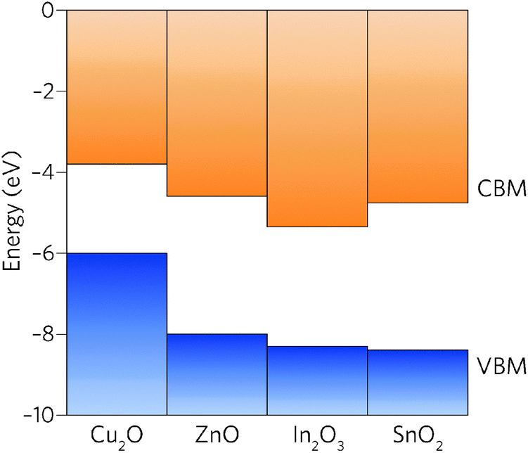 | ||
| Fig. 1 Valence and conduction band offsets between Cu2O, ZnO, In2O3 and SnO2 taken from recent experiments37 and calculations.32,38 The vacuum level is set to 0 eV. | ||
Band gap modulation in semiconductors can be achieved in a number of ways, including chemical doping,42 strain engineering,43 and inducing lattice disorder.44,45 Band gap engineering in In2O3 was recently demonstrated by alloying with Tl2O3.46 As both compounds crystallise in the same structure, incorporation of Tl resulted in a monotonic decrease of the band gap without otherwise affecting the electronic structure. The desired properties of the material best suited for alloying with SnO2 are therefore: (i) a smaller band gap, (ii) a highly dispersed conduction band, and (iii) a compound that crystallises in the rutile crystal structure.
Of the group 14 oxides, PbO2 is isostructural and isoelectronic to SnO2 and therefore likely to allow for efficient alloying. Furthermore, it was recently identified as a narrow band gap semiconductor, with a conduction band dominated by low-lying Pb s states due to relativistic effects.47 The electronic structure of the conduction band of PbO2 is nearly ideal for a TCO, with a low electron effective mass of 0.18me and a very large separation between the CBM and the CBM + 1. The fundamental band gap, however, is too small for transparency when undoped. Oxygen substoichiometry48,49 and possibly adventitious hydrogen50–52 cause the Fermi level to sit far above the CBM of PbO2, leading to high levels of conductivity. Furthermore, it has even been suggested that through tuning of the Fermi level position in the conduction band, PbO2 could be transformed into a TCO itself.53 Pb is also significantly more abundant and less expensive than Sn,54 and as such PbO2 was considered the ideal compound to incorporate into SnO2.
In this Article we propose incorporation of Pb as an efficient method of modulating the band gap of SnO2. Using hybrid density functional theory (DFT) we demonstrate that the fundamental band gap of Sn1−xPbxO2 (0 ≤ x ≤ 0.125) can be tuned from ∼3.67 eV to 3.17 eV. The enthalpy of mixing is shown to be favourable at moderately high temperatures, suggesting the system can be achieved experimentally. Crucially, band gap modulation occurs primarily through lowering of the CBM relative to the vacuum level, thereby increasing the electron affinity. The ability to modulate the band gap – and consequently work function – has significant implications in the field of organic photovoltaics, in which the work function alignment of the cathode and hole injection layer is essential to form an Ohmic contact and increase the built-in potential of the interface.
Methodology
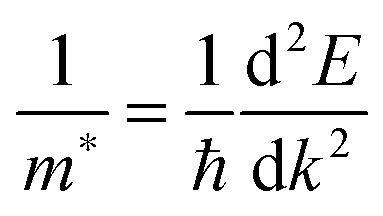
All our DFT calculations were performed using the Vienna Ab initio Simulation Package (VASP),55–58 with interactions between the core (Sn:[Kr], Pb:[Xe], and O:[He]) and valence electrons described using the Projector Augmented Wave method.59 Two different functionals were employed: PBEsol,60 a version of the Generalised Gradient Approximation (GGA) PBE61 functional revised for solids and PBE0, a hybrid density functional proposed by Adamo and Barone.62 In the PBE0 approach, 25% exact Hartree–Fock (HF) exchange is combined with 75% exchange and the correlation energies from PBE.61 PBEsol is known to accurately predict lattice constants for solid state systems, while PBE0 reproduces the band gap and electronic structure of SnO2 seen in experiment.21,63,64 PBE0 also replicates the recently confirmed semiconductor nature of PbO2.47Both k-point sampling and the plane wave basis set were checked for convergence, with a cutoff of 450 eV and k-point grid of Γ-centred 4 × 4 × 6, for the 6 atom unit cells of SnO2 and PbO2, found to be sufficient. The structures were geometrically optimized and deemed to be converged when the forces on all the atoms totalled less than 10 meV Å−1. Optical absorption spectra were determined using the optical transition matrix elements calculated within the transversal approximation.65 This approach sums the absorption spectra over all direct valence to conduction band transitions and, as such, does not account for indirect and intraband absorptions.66 Supercell calculations, due to shrinking of the Brillouin zone, result in folded band structures that can be difficult to interpret. To prevent this, primitive cell representations of supercell band structures were obtained using the band unfolding code BandUp,67,68 based on the methodolgy described by Popescu and Zunger.69 Electron effective masses at the band edges were calculated according to:
 | (1) |
 is the curvature of the band at the CBM.
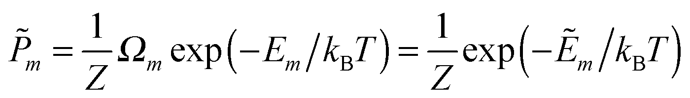
In this work we investigate the thermodynamics of alloying and select the lowest energy alloy structures at particular compositions. Investigations into configuration effects in solid solutions are complicated by the large number of possible structures that can exist for a particular supercell. To avoid this problem we have followed the procedure implemented in the Site Occupancy Disorder (SOD) program developed by De Leeuw and co-workers.70 Here, the complete configurational space for each supercell composition is generated, from which the subspace of symmetrically inequivalent configurations can be extracted. This method is able to reduce the computational complexity by several orders of magnitude, making previously prohibitive problems tractable. The process of calculating the configurational averages and entropies has been explained in more detail elsewhere in the literature,71,72 but is based on the assumption that a Boltzmann-like probability can predict the extent of occurrence of a particular configuration. This takes into account both the energy, Em, of the configuration and its degeneracy, Ωm, i.e. how many times the configuration appears in the complete configurational space:
 | (2) |
 | (3) |
G = −kT![[thin space (1/6-em)]](https://www.rsc.org/images/entities/char_2009.gif) lnZ lnZ | (4) |
Results and discussion
SnO2 and β-PbO2 (mineral names, cassiterite and plattnerite) both crystallise in the rutile crystal structure, containing 6 atoms in a unit cell.73 The cation is coordinated to six oxygen in a distorted octahedron (D4h symmetry), with each oxygen coordinated to three cations by one short and two long bonds. The PBEsol calculated a and c lattice parameters for SnO2 were 4.772 Å and 3.216 Å respectively. These are in close agreement (within 0.9%) with neutron diffraction experiments.74,75 In order to calculate the electronic properties of SnO2, the structure was relaxed using PBE0, after which the electronic structure was calculated, again using PBE0. The fundamental band gap of SnO2 was found to be 3.67 eV. This is very similar to the experimentally observed fundamental band gap of 3.59 eV.76–78 We note that this experimental measurement has not been performed in the traditional way (i.e. the ionisation potential – electron affinity, measured, for instance using inverse photoemission spectroscopy) but instead has been measured using two-photon spectroscopy and factors in the known exciton binding energy in SnO2 of 30 meV.79–81 The valence band maximum (VBM) and CBM both occur at the Γ point, resulting in a fundamental band gap that is direct. For PbO2 the calculated lattice parameters were 4.994 Å and 3.416 Å, for a and c respectively. These again closely matched experimental results (within 1.0%).82,83 The semiconductor nature of PbO2 was reproduced in the PBE0 calculated direct band gap of 0.64 eV, which again was calculated from the PBE0-relaxed structure. However, due to large carrier concentrations and the relative lack of optical measurements in the literature, the exact magnitude of the experimental band gap.84,85To investigate the effects of alloying, we have considered the substitution of Sn by Pb in a 2 × 2 × 2 (48 atom) supercell of SnO2 containing 16 cation sites. Table 1 shows the total (N) and symmetrically inequivalent (M) number of configurations as a function of Pb concentration (Sn16−nPbnO32 where n = 0, 1, 2, …, 16). The equilibrium geometries and energies of all inequivalent configurations were calculated using PBEsol as described above. An analysis of the results reveals that, for each composition, the difference in energy between the most and least stable configurations is very small, at most 16 meV per atom. As such, a disordered alloy is more likely to form rather than an ordered solid solution.
| N Pb | x | N | M |
|---|---|---|---|
| 0 | 0.000 | 1 | 1 |
| 1 | 0.062 | 16 | 1 |
| 2 | 0.125 | 120 | 6 |
| 3 | 0.188 | 560 | 13 |
| 4 | 0.250 | 1820 | 41 |
| 5 | 0.312 | 4368 | 65 |
| 6 | 0.375 | 8008 | 120 |
| 7 | 0.438 | 11440 |
145 |
| 8 | 0.500 | 12870 |
180 |
| 9 | 0.562 | 11440 |
145 |
| 10 | 0.625 | 8008 | 120 |
| 11 | 0.688 | 4368 | 65 |
| 12 | 0.750 | 1820 | 41 |
| 13 | 0.812 | 560 | 13 |
| 14 | 0.875 | 120 | 6 |
| 15 | 0.938 | 16 | 1 |
| 16 | 1.000 | 1 | 1 |
| Total | 65535 |
963 |
To study the stability of the alloys against that of the individual components, the enthalpies and free energies of mixing were calculated as a function of composition, across a range of temperatures, as:
| ΔHmix = E(Sn1−xPbxO2) − (1 − x)E(SnO2) − xE(PbO2) | (5) |
| ΔGmix = G(Sn1−xPbxO2) − (1 − x)E(SnO2) − xE(PbO2) | (6) |
Fig. 2a shows the results plotted as a function of composition. The enthalpy of mixing is small but positive, indicating that the mixing is a slightly exothermic process. The free energy of mixing turns negative at temperatures greater than 850 K (580 °C), for compositions where x = 0.062 and 0.125, indicating that the structures formed will be thermodynamically stable. The lines corresponding to 850 K and 1050 K contain two minima, one at Sn-rich and another at Pb-rich compositions, highlighting that any intermediate compositions would separate into two phases if kinetically allowed.86,87 At higher temperatures this thermodynamic miscibility gap disappears due to increasing contribution from the entropic term.
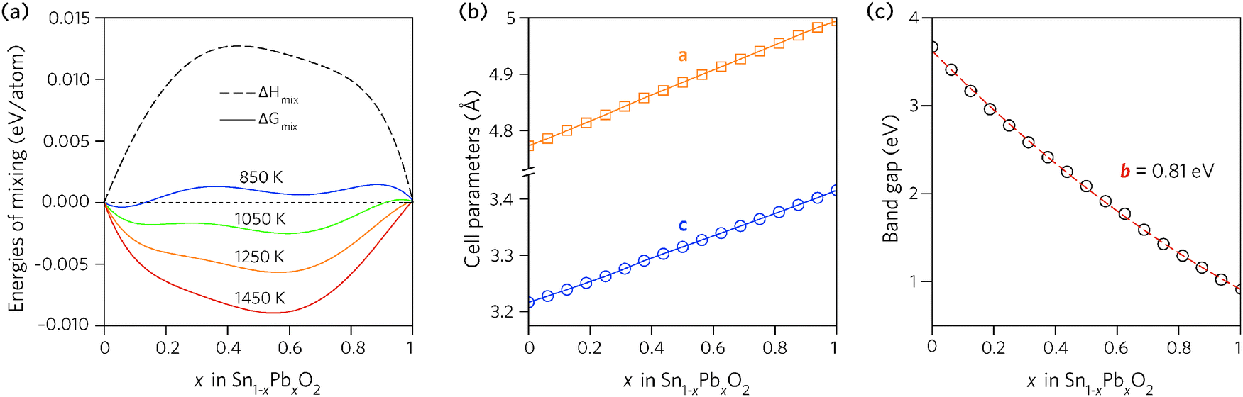 | ||
| Fig. 2 Trends across the full composition space of Sn1−xPbxO2 for: (a) the enthalpy and free energy of mixing, (b) the unit cell lattice parameters, and (c) the direct fundamental band gaps (Edirg). | ||
The dependence of the calculated lattice parameters on composition is shown in Fig. 2b. Each point represents the average lattice constant across the entire configurational space for that composition, with the assumption of full disorder. This discounts any preference for ordering of the cations, however, as the difference in energy between configurations is small, the change in the average lattice parameters will be negligible. The lattice constants of the alloy display a linear increase with increasing Pb concentration, as expected due to the increase in atomic radius from Sn to Pb, and following Vegard's law.88
In order to find the optimum doping levels, the band gap trend of the alloys was investigated. To calculate the electronic properties of almost 1000 structures accurately would have been prohibitively resource intensive. Instead, the lowest energy configurations at each composition were geometrically relaxed using the PBE0 functional, after which the electronic structures were calculated, again using PBE0. Fig. 2c shows the band gaps of the lowest energy alloy structures at each composition. The alloy band gaps decrease monotonically with increasing Pb concentration, from 3.37 eV at x = 0.062 to 0.74 eV at x = 0.938. The decrease is not linear, indeed the band gap bowing parameter, defined from:
| Eg(x) = (1 − x)Eg(SnO2) + xEg(PbO2) − bx(1 − x) | (7) |
To see how alloying affects the band structure, we have calculated the “effective” primitive cell band structure using the PBE0 functional and BandUp code, as described above. Fig. 3 shows a comparison between the band structures of undoped SnO2 and the two doping concentrations, where the direct band gap (Z to Γ to M) is shown. The alloys have maintained the ideal electronic structure needed for an efficient TCO, with the band gap reduction immediately obvious. Furthermore, the dispersion at the band edges remains excellent, indicating high carrier mobilities. The calculated electron effective mass at the CBM decreases with Pb concentration, from 0.27me to 0.26me, for Sn0.938Pb0.062O2 and Sn0.875Pb0.125O2 respectively. This is an improvement on undoped SnO2, which has a calculated effective mass of 0.28me, in excellent agreement with experiment (0.29me).91
 | ||
| Fig. 3 The calculated effective band structure for Sn1−xPbxO2 where x = 0.00, 0.06, and 0.12. The conduction bands are coloured orange whereas the valence bands are shown in blue, with the VBM is set to 0 eV in each case. | ||
A simple band alignment derived from an O 1s level is displayed in Fig. 4.92–95 Band alignments relative to the band positions of SnO2 provide useful informational about the nature of the band gap changes.96–99 It is clear that the reduction in band gap occurs overwhelming through lowering of the CBM relative to the vacuum level, in the case of Sn0.875Pb0.125O2 by 0.592, effectively increasing the EA. This is due to the relativistic contraction of the Pb 6s orbitals, which increases their stability and causes these states appear at lower energies relative to the vacuum level. This indicates that Pb doped SnO2 should display an increased n-type dopability and, as such, could possess increased carrier concentrations when donor doped. Unexpectedly, the VBM also decreases slightly with increasing Pb concentration. Based on the increased Pb d–O 2p repulsion in PbO2 relative to the Sn d–O 2p repulsion in SnO2, the VBM of the alloys would generally have been expected to rise. It is possible that this is an artefact of the simplified alignment model, however, the large modulation of the CBM is to be expected.
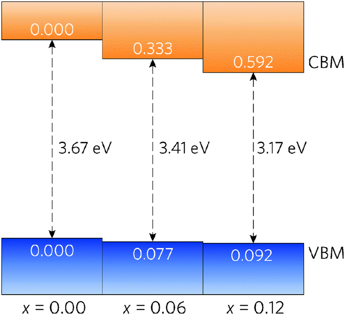 | ||
| Fig. 4 Band alignment for Sn1−xPbxO2, where x = 0.00, 0.06, and 0.12. All energies are given relative to a O 1s state. | ||
Having established that Pb incorporation decreases the fundamental band gap of SnO2, it is instructive to investigate the effects of the alloying on optical properties. As the inversion symmetry of the lattice results in disallowed transitions at the Γ point, the optical band gaps (Eoptg) of SnO2 and PbO2 are considerably widened relative to the fundamental band gaps.47,79,81,100 The optical absorption spectra for SnO2, Sn0.938Pb0.062O2 and Sn0.875Pb0.125O2, calculated using PBE0 from the frequency dependent dielectric matrix, are presented in Fig. 5. We can clearly see that incorporation of Pb does not affect the disallowed nature of the optical band gaps, as in all cases the optical band gaps are significantly larger than the fundamental band gaps, indicating that the Sn1−xPbxO2 alloys will retain high levels of optical transparency.
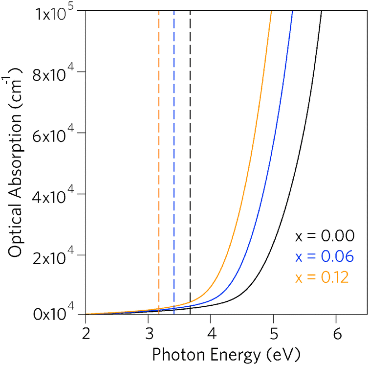 | ||
| Fig. 5 Calculated optical absorption spectra for Sn1−xPbxO2 where x = 0.00, 0.06, and 0.12. Full lines indicate optical absorption and dashed lines indicate fundamental band gap. | ||
Conclusions
In this study we set out to tailor the band gap of SnO2 in order to improve its performance as a transparent conducting oxide. Our approach was centred around reducing the band gap by decreasing the position of the conduction band minimum, thereby increasing the electron affinity and thus increasing the dopability.18,46 To be effective, the fundamental band gap of the improved SnO2 material must be greater than 3.1 eV whilst no detrimental effects on the effective mass at the conduction band minimum should be seen, in the interest of retaining high electron mobilities.Through alloying with isoelectronic and isostructural PbO2, we have demonstrated that the band gaps of Sn1−xPbxO2 alloys can be tuned from 3.67 eV to 0.64 eV with increasing Pb content, arising from stabilization of the conduction band minimum relative to the vacuum level. We have found that Sn0.875Pb0.125O2 displays a fundamental band gap that is just above 3.1 eV, possesses effective masses that are lower than for pure SnO2, and has an electron affinity 0.59 eV larger than SnO2. Furthermore, the optical transparency of this alloy remains extremely high. These properties should therefore, in principle, make SnO2:Pb a more efficient n-type transparent material and an ideal candidate for use in TCO applications.101
Additionally, as lowering of the conduction band minimum results in an increase in the work function (provided the Fermi level remains near to the band edges), these results demonstrate the possibility of a single generic system, in which the work function can be finely tuned over a wide range, based only on single parameter. This poses significant advantages for organic solar cells, which require efficient alignment between the work functions of the cathode and hole injection layer in order to produce an Ohmic contact and maximise device efficiency. As such, we stress the pressing need for experimental verification of these results.
Acknowledgements
This work made use of the ARCHER UK National Supercomputing Service (http://www.archer.ac.uk), via our membership of the UK's HEC Materials Chemistry Consortium, which is funded by EPSRC (EP/L000202) and the UCL Legion HPC Facility (Legion@UCL). The work at UCL was supported by EPSRC (EP/N01572X/1). DOS acknowledges support from the SUPERSOLAR Solar Energy Hub (EP/J017361/1) for the provision of a flexible funding call award. AMG acknowledges Diamond Light Source for the co-sponsorship of a studentship on the EPSRC Centre for Doctoral Training in Molecular Modelling and Materials Science (EP/L015862/1).References
- C. Hogarth, Hall Constant of Cadmium Oxide, Nature, 1951, 167, 521–522 CrossRef CAS PubMed.
- B. G. Lewis and D. C. Paine, Applications and processing of transparent conducting oxides, MRS Bull., 2000, 25, 22–27 CrossRef CAS.
- A. Porch, D. V. Morgan, R. M. Perks, M. O. Jones and P. P. Edwards, Electromagnetic absorption in transparent conducting films, J. Appl. Phys., 2004, 95, 4734–4737 CrossRef CAS.
- A. N. Tiwari, G. Khrypunov, F. Kurdzesau, D. Bätzner, A. Romeo and H. Zogg, CdTe solar cell in a novel configuration, Prog. Photovoltaics, 2004, 12, 33–38 CAS.
- I. Hamberg and C. G. Granqvist, Evaporated Sn-doped In2O3 films: basic optical properties and applications to energy-efficient windows, J. Appl. Phys., 1986, 60, 123–160 CrossRef.
- C. Granqvist and A. Hultåker, Transparent and conducting ITO films: new developments and applications, Thin Solid Films, 2002, 411, 1–5 CrossRef CAS.
- H. Van Oss, US Geological Survey, Mineral Commodity Summaries, 2014; http://minerals.usgs.gov/minerals/pubs/commodity/indium/mcs-2014-indiu.pdf.
- M. Burbano, D. O. Scanlon and G. W. Watson, Sources of conductivity and doping limits in CdO from hybrid density functional theory, J. Am. Chem. Soc., 2011, 133, 15065–15072 CrossRef CAS PubMed.
- T. Minami and T. Miyata, Present status and future prospects for development of non-or reduced-indium transparent conducting oxide thin films, Thin Solid Films, 2008, 517, 1474–1477 CrossRef CAS.
- S. Sallis, D. Scanlon, S. Chae, N. Quackenbush, D. Fischer, J. Woicik, J.-H. Guo, S. Cheong and L. Piper, La-doped BaSnO3 – Degenerate perovskite transparent conducting oxide: evidence from synchrotron X-ray spectroscopy, Appl. Phys. Lett., 2013, 103, 042105 CrossRef.
- T. Minami, Transparent conducting oxide semiconductors for transparent electrodes, Semicond. Sci. Technol., 2005, 20, S35 CrossRef CAS.
- E. Burstein, Anomalous optical absorption limit in InSb, Phys. Rev., 1954, 93, 632 CrossRef CAS.
- T. Moss, The interpretation of the properties of indium antimonide, Proc. Phys. Soc., London, Sect. B, 1954, 67, 775 CrossRef.
- S. Shanthi, C. Subramanian and P. Ramasamy, Investigations on the optical properties of undoped, fluorine doped and antimony doped tin oxide films, Cryst. Res. Technol., 1999, 34, 1037–1046 CrossRef CAS.
- S. Zhang, S. Wei and A. Zunger, A phenomenological model for systematization and prediction of doping limits in II–VI and I–III–VI2 compounds, J. Appl. Phys., 1998, 83, 3192–3196 CrossRef CAS.
- S. Zhang, S.-H. Wei and A. Zunger, Overcoming doping bottlenecks in semiconductors and wide-gap materials, Phys. B, 1999, 273, 976–980 CrossRef.
- S. Zhang, The microscopic origin of the doping limits in semiconductors and wide-gap materials and recent developments in overcoming these limits: a review, J. Phys.: Condens. Matter, 2002, 14, 881 CrossRef.
- A. Walsh, J. Buckeridge, C. R. A. Catlow, A. J. Jackson, T. W. Keal, M. Miskufova, P. Sherwood, S. A. Shevlin, M. B. Watkins, S. M. Woodley and A. A. Sokol, Limits to Doping of Wide Band Gap Semiconductors, Chem. Mater., 2013, 25, 2924–2926 CrossRef CAS.
- P. P. Edwards, A. Porch, M. O. Jones, D. V. Morgan and R. M. Perks, Basic materials physics of transparent conducting oxides, Dalton Trans., 2004, 2995–3002 RSC.
- E. Fortunato, D. Ginley, H. Hosono and D. C. Paine, Transparent conducting oxides for photovoltaics, MRS Bull., 2007, 32, 242–247 CrossRef CAS.
- M. Batzill and U. Diebold, The surface and materials science of tin oxide, Prog. Surf. Sci., 2005, 79, 47–154 CrossRef CAS.
- G. Sanon, R. Rup and A. Mansingh, Band-gap narrowing and band structure in degenerate tin oxide (SnO2) films, Phys. Rev. B: Solid State, 1991, 44, 5672 CrossRef CAS.
- Z. Hu and S. Gao, Upper crustal abundances of trace elements: a revision and update, Chem. Geol., 2008, 253, 205–221 CrossRef CAS.
- R. G. Gordon, Criteria for choosing transparent conductors, MRS Bull., 2000, 25, 52–57 CrossRef CAS.
- M.-M. Bagheri-Mohagheghi and M. Shokooh-Saremi, The influence of Al doping on the electrical, optical and structural properties of SnO2 transparent conducting films deposited by the spray pyrolysis technique, J. Phys. D: Appl. Phys., 2004, 37, 1248 CrossRef CAS.
- K. Omura, P. Veluchamy, M. Tsuji, T. Nishio and M. Murozono, A Pyrosol Technique to Deposit Highly Transparent, Low-Resistance SnO2: F Thin Films from Dimethyltin Dichloride, J. Electrochem. Soc., 1999, 146, 2113–2116 CrossRef CAS.
- R. Binions, C. J. Carmalt and I. P. Parkin, A comparison of the gas sensing properties of solid state metal oxide semiconductor gas sensors produced by atmospheric pressure chemical vapour deposition and screen printing, Meas. Sci. Technol., 2007, 18, 190 CrossRef CAS.
- N. Noor and I. P. Parkin, Enhanced transparent-conducting fluorine-doped tin oxide films formed by Aerosol-Assisted Chemical Vapour Deposition, J. Mater. Chem. C, 2013, 1, 984–996 RSC.
- Ç. Klç and A. Zunger, Origins of coexistence of conductivity and transparency in SnO2, Phys. Rev. Lett., 2002, 88, 095501 CrossRef PubMed.
- D. O. Scanlon, Defect engineering of BaSnO3 for high-performance transparent conducting oxide applications, Phys. Rev. B: Condens. Matter Mater. Phys., 2013, 87, 161201 CrossRef.
- A. K. Singh, A. Janotti, M. Scheffler and C. G. Van de Walle, Sources of electrical conductivity in SnO2, Phys. Rev. Lett., 2008, 101, 055502 CrossRef PubMed.
- D. O. Scanlon and G. W. Watson, On the possibility of p-type SnO2, J. Mater. Chem., 2012, 22, 25236–25245 RSC.
- K. Xiong, J. Robertson and S. Clark, Behavior of hydrogen in wide band gap oxides, J. Appl. Phys., 2007, 102, 083710 CrossRef.
- P. King, R. Lichti, Y. Celebi, J. Gil, R. Vilão, H. Alberto, J. P. Duarte, D. Payne, R. Egdell and I. McKenzie, Shallow donor state of hydrogen in In2O3 and SnO2: implications for conductivity in transparent conducting oxides, Phys. Rev. B: Condens. Matter Mater. Phys., 2009, 80, 081201 CrossRef.
- W. H. Oo, S. Tabatabaei, M. McCluskey, J. Varley, A. Janotti and C. Van de Walle, Hydrogen donors in SnO2 studied by infrared spectroscopy and first-principles calculations, Phys. Rev. B: Condens. Matter Mater. Phys., 2010, 82, 193201 CrossRef.
- P. D. C. King and T. D. Veal, Conductivity in transparent oxide semiconductors, J. Phys.: Condens. Matter, 2011, 23, 334214 CrossRef CAS PubMed.
- B. Kramm, A. Laufer, D. Reppin, A. Kronenberger, P. Hering, A. Polity and B. K. Meyer, The band alignment of Cu2O/ZnO and Cu2O/GaN heterostructures, Appl. Phys. Lett., 2012, 100, 094102 CrossRef.
- B. Höffling, A. Schleife, C. Rödl and F. Bechstedt, Band discontinuities at Si-TCO interfaces from quasiparticle calculations: Comparison of two alignment approaches, Phys. Rev. B: Condens. Matter Mater. Phys., 2012, 85, 035305 CrossRef.
- A. Walsh and D. O. Scanlon, Polymorphism of indium oxide: materials physics of orthorhombic In2O3, Phys. Rev. B: Condens. Matter Mater. Phys., 2013, 88, 161201 CrossRef.
- A. Klein, C. Körber, A. Wachau, F. Säuberlich, Y. Gassenbauer, S. P. Harvey, D. E. Proffit and T. O. Mason, Transparent conducting oxides for photovoltaics: manipulation of Fermi level, work function and energy band alignment, Materials, 2010, 3, 4892–4914 CrossRef CAS.
- J. Bellingham, W. Phillips and C. Adkins, Intrinsic performance limits in transparent conducting oxides, J. Mater. Sci. Lett., 1992, 11, 263–265 CrossRef CAS.
- M. H. Harunsani, F. E. Oropeza, R. G. Palgrave and R. G. Egdell, Electronic and Structural Properties of SnxTi1−xO2 (0.0 ≤ x ≤ 0.1) Solid Solutions, Chem. Mater., 2010, 22, 1551–1558 CrossRef CAS.
- W. Zhou, Y. Liu, Y. Yang and P. Wu, Band gap engineering of SnO2 by epitaxial strain: experimental and theoretical investigations, J. Phys. Chem. C, 2014, 118, 6448–6453 CAS.
- D. O. Scanlon and A. Walsh, Bandgap engineering of ZnSnP2 for high-efficiency solar cells, Appl. Phys. Lett., 2012, 100, 251911 CrossRef.
- N. Feldberg, J. Aldous, W. Linhart, L. Phillips, K. Durose, P. Stampe, R. Kennedy, D. Scanlon, G. Vardar and R. Field III, Growth, disorder, and physical properties of ZnSnN2, Appl. Phys. Lett., 2013, 103, 042109 CrossRef.
- D. O. Scanlon, A. Regoutz, R. G. Egdell, D. J. Morgan and G. W. Watson, Band gap engineering of In2O3 by alloying with Tl2O3, Appl. Phys. Lett., 2013, 103, 2011–2015 CrossRef.
- D. O. Scanlon, A. B. Kehoe, G. W. Watson, M. O. Jones, W. I. David, D. J. Payne, R. G. Egdell, P. P. Edwards and A. Walsh, Nature of the band gap and origin of the conductivity of PbO2 revealed by theory and experiment, Phys. Rev. Lett., 2011, 107, 246402 CrossRef PubMed.
- A. Walsh, J. L. Da Silva and S.-H. Wei, Origins of band-gap renormalization in degenerately doped semiconductors, Phys. Rev. B: Condens. Matter Mater. Phys., 2008, 78, 075211 CrossRef.
- P. Moseley, J. Hutchison and M. Bourke, The Defect Structure of Lead Dioxide, J. Electrochem. Soc., 1982, 129, 876–880 CrossRef CAS.
- W. Mindt, Electrical properties of electrodeposited PbO2 films, J. Electrochem. Soc., 1969, 116, 1076–1080 CrossRef CAS.
- P. Rüetschi, Influence of crystal structure and interparticle contact on the capacity of PbO2 electrodes, J. Electrochem. Soc., 1992, 139, 1347–1351 CrossRef.
- P. Moseley, J. Hutchison, C. Wright, M. Bourke, R. Hill and V. Rainey, Inelastic neutron scattering and transmission electron microscope studies of lead dioxide, J. Electrochem. Soc., 1983, 130, 829–834 CrossRef CAS.
- A. Walsh, A. B. Kehoe, D. J. Temple, G. W. Watson and D. O. Scanlon, PbO2: from semi-metal to transparent conducting oxide by defect chemistry control, Chem. Commun., 2013, 49, 448–450 RSC.
- S. Taylor, Abundance of chemical elements in the continental crust: a new table, Geochim. Cosmochim. Acta, 1964, 28, 1273–1285 CrossRef CAS.
- G. Kresse and J. Hafner, Ab initio molecular dynamics for liquid metals, Phys. Rev. B: Condens. Matter Mater. Phys., 1993, 47, 558–561 CrossRef CAS.
- G. Kresse and J. Hafner, Ab initio molecular-dynamics simulation of the liquid-metal amorphous-semiconductor transition in germanium, Phys. Rev. B: Condens. Matter Mater. Phys., 1994, 49, 14251–14269 CrossRef CAS.
- G. Kresse and J. Furthmüller, Efficient iterative schemes for ab initio total-energy calculations using a plane-wave basis set, Phys. Rev. B: Condens. Matter Mater. Phys., 1996, 54, 11169–11186 CrossRef CAS.
- G. Kresse and J. Furthmüller, Efficiency of ab initio total energy calculations for metals and semiconductors using a plane wave basis set, Comput. Mater. Sci., 1996, 6, 15 CrossRef CAS.
- G. Kresse and D. Joubert, From ultrasoft pseudopotentials to the projector augmented-wave method, Phys. Rev. B: Condens. Matter Mater. Phys., 1999, 59, 1758 CrossRef CAS.
- J. P. Perdew, A. Ruzsinszky, G. I. Csonka, O. A. Vydrov, G. E. Scuseria, L. A. Constantin, X. Zhou and K. Burke, Restoring the density-gradient expansion for exchange in solids and surfaces, Phys. Rev. Lett., 2008, 100, 136406 CrossRef PubMed.
- J. Perdew, K. Burke and M. Ernzerhof, Generalized Gradient Approximation Made Simple, Phys. Rev. Lett., 1996, 77, 3865–3868 CrossRef CAS PubMed.
- C. Adamo and V. Barone, Toward reliable density functional methods without adjustable parameters: The PBE0 model, J. Chem. Phys., 1999, 110, 6158 CrossRef CAS.
- P. Ágoston, K. Albe, R. M. Nieminen and M. J. Puska, Intrinsic n-type behavior in transparent conducting oxides: A comparative hybrid-functional study of In2O3, SnO2, and ZnO, Phys. Rev. Lett., 2009, 103, 245501 CrossRef PubMed.
- S. V. Farahani, T. D. Veal, J. J. Mudd, D. Scanlon, G. Watson, O. Bierwagen, M. White, J. S. Speck and C. F. McConville, Valence-band density of states and surface electron accumulation in epitaxial SnO2 films, Phys. Rev. B: Condens. Matter Mater. Phys., 2014, 90, 155413 CrossRef.
- M. Gajdoš, K. Hummer, G. Kresse, J. Furthmüller and F. Bechstedt, Linear optical properties in the projector-augmented wave methodology, Phys. Rev. B: Condens. Matter Mater. Phys., 2006, 73, 045112 CrossRef.
- B. Adolph, J. Furthmüller and F. Bechstedt, Optical properties of semiconductors using projector-augmented waves, Phys. Rev. B: Condens. Matter Mater. Phys., 2001, 63, 125108 CrossRef.
- P. V. Medeiros, S. Stafström and J. Björk, Effects of extrinsic and intrinsic perturbations on the electronic structure of graphene: Retaining an effective primitive cell band structure by band unfolding, Phys. Rev. B: Condens. Matter Mater. Phys., 2014, 89, 041407 CrossRef.
- P. V. Medeiros, S. S. Tsirkin, S. Stafström and J. Björk, Unfolding spinor wave functions and expectation values of general operators: Introducing the unfolding-density operator, Phys. Rev. B: Condens. Matter Mater. Phys., 2015, 91, 041116 CrossRef.
- V. Popescu and A. Zunger, Extracting E versus
![[k with combining right harpoon above (vector)]](https://www.rsc.org/images/entities/i_char_006b_20d1.gif) effective band structure from supercell calculations on alloys and impurities, Phys. Rev. B: Condens. Matter Mater. Phys., 2012, 85, 085201 CrossRef.
effective band structure from supercell calculations on alloys and impurities, Phys. Rev. B: Condens. Matter Mater. Phys., 2012, 85, 085201 CrossRef. - R. Grau-Crespo, S. Hamad, C. Catlow and N. De Leeuw, Symmetry-adapted configurational modelling of fractional site occupancy in solids, J. Phys.: Condens. Matter, 2007, 19, 256201 CrossRef.
- I. Todorov, N. Allan, M. Y. Lavrentiev, C. Freeman, C. Mohn and J. Purton, Simulation of mineral solid solutions at zero and high pressure using lattice statics, lattice dynamics and Monte Carlo methods, J. Phys.: Condens. Matter, 2004, 16, 2751 CrossRef.
- S. Benny, R. Grau-Crespo and N. H. de Leeuw, A theoretical investigation of α-Fe2O3–Cr2O3 solid solutions, Phys. Chem. Chem. Phys., 2009, 11, 808–815 RSC.
- W. H. Baur and A. A. Khan, Rutile-type compounds. IV. SiO2, GeO2 and a comparison with other rutile-type structures, Acta Crystallogr., Sect. B: Struct. Crystallogr. Cryst. Chem., 1971, 27, 2133–2139 CrossRef CAS.
- T. Yamanaka, R. Kurashima and J. Mimaki, X-ray diffraction study of bond character of rutile-type SiO2, GeO2 and SnO2, Z. Kristallogr., 2000, 215, 424 CAS.
- J. Haines and J. Leger, X-ray diffraction study of the phase transitions and structural evolution of tin dioxide at high pressure: Relationships between structure types and implications for other rutile-type dioxides, Phys. Rev. B: Condens. Matter Mater. Phys., 1997, 55, 11144 CrossRef CAS.
- K. Reimann and M. Steube, Experimental determination of the electronic band structure of SnO2, Solid State Commun., 1998, 105, 649–652 CrossRef CAS.
- D. Fröhlich, R. Kenklies and R. Helbig, Band-Gap Assignment in SnO2 by Two-Photon Spectroscopy, Phys. Rev. Lett., 1978, 41, 1750 CrossRef.
- M. Feneberg, C. Lidig, K. Lange, R. Goldhahn, M. D. Neumann, N. Esser, O. Bierwagen, M. E. White, M. Y. Tsai and J. S. Speck, Ordinary and extraordinary dielectric functions of rutile SnO2 up to 20 eV, Appl. Phys. Lett., 2014, 104, 231106 CrossRef.
- M. Nagasawa and S. Shionoya, Exciton structure in optical absorption of SnO2 crystals, Phys. Lett., 1966, 22, 409–410 CrossRef CAS.
- V. Agekyan, Spectroscopic Properties of Semiconductor Crystals with Direct Forbidden Energy Gap, Phys. Status Solidi A, 1977, 43, 11–42 CrossRef CAS.
- A. Schleife, J. Varley, F. Fuchs, C. Rödl, F. Bechstedt, P. Rinke, A. Janotti and C. Van de Walle, Tin dioxide from first principles: quasiparticle electronic states and optical properties, Phys. Rev. B: Condens. Matter Mater. Phys., 2011, 83, 035116 CrossRef.
- H. Harada, Y. Sasa and M. Uda, Crystal data for β-PbO2, J. Appl. Crystallogr., 1981, 14, 141–142 CrossRef CAS.
- D. Taylor, Thermal expansion data. II: binary oxides with the fluorite and rutile structures, MO2, and the antifluorite structure, M2O, Trans. J. Br. Ceram. Soc., 1984, 83, 32–37 CAS.
- J. P. Pohl and G. L. Schlechtriemen, Concentration, mobility and thermodynamic behaviour of the quasi-free electrons in lead dioxide, J. Appl. Electrochem., 1984, 14, 521–531 CrossRef CAS.
- D. J. Payne, R. G. Egdell, W. Hao, J. S. Foord, A. Walsh and G. W. Watson, Why is lead dioxide metallic?, Chem. Phys. Lett., 2005, 411, 181–185 CrossRef CAS.
- I.-h. Ho and G. Stringfellow, Solid phase immiscibility in GaInN, Appl. Phys. Lett., 1996, 69, 2701–2703 CrossRef CAS.
- S. Chen, A. Walsh, J.-H. Yang, X. Gong, L. Sun, P.-X. Yang, J.-H. Chu and S.-H. Wei, Compositional dependence of structural and electronic properties of Cu2ZnSn(S,Se)4 alloys for thin film solar cells, Phys. Rev. B: Condens. Matter Mater. Phys., 2011, 83, 125201 CrossRef.
- L. Vegard, Die konstitution der mischkristalle und die raumfüllung der atome, Z. Phys. A: Hadrons Nucl., 1921, 5, 17–26 CAS.
- J. Phillips, Bonds and bands in semiconductors, Elsevier, 2012 Search PubMed.
- A. Czapla, M. Jachimowski, E. Kusior and J. Szczyrbowski, Optical properties of PbxSn1−xO2 Films, Phys. Status Solidi A, 1978, 45, 537–542 CrossRef CAS.
- K. J. Button, C. G. Fonstad and W. Dreybrodt, Determination of the electron masses in stannic oxide by submillimeter cyclotron resonance, Phys. Rev. B: Solid State, 1971, 4, 4539 CrossRef.
- D. O. Scanlon, K. G. Godinho, B. J. Morgan and G. W. Watson, Understanding Conductivity Anomalies in CuI-Based Delafossite Transparent Conducting Oxides: Theoretical Insights, J. Chem. Phys., 2010, 132, 024707 CrossRef PubMed.
- S.-H. Wei and A. Zunger, Calculated Natural Band Offsets of All II–VI and III–V Semiconductors: Chemical Trends and the Role of Cation d Orbitals, Appl. Phys. Lett., 2011, 72, 1998 Search PubMed.
- M. C. Toroker and E. A. Carter, Transition Metal Oxide Alloys as Potential Solar Energy Conversion Materials, J. Mater. Chem. A, 2013, 1, 2474–2484 CAS.
- C.-K. Tan and N. Tansu, First-Principle Natural Band Alignment of GaN/Dilute-As GaNAs Alloy, AIP Adv., 2015, 5, 017129 CrossRef.
- D. O. Scanlon, C. W. Dunnill, J. Buckeridge, S. A. Shevlin, A. J. Logsdail, S. M. Woodley, C. R. A. Catlow, M. J. Powell, R. G. Palgrave, I. P. Parkin, G. W. Watson, T. W. Keal, P. Sherwood, A. Walsh and A. A. Sokol, et al., Band Alignment of Rutile and Anatase TiO2, Nat. Mater., 2013, 12, 798–801 CrossRef CAS PubMed.
- Y. Wu, M. Chan and G. Ceder, Prediction of Semiconductor Band Edge Positions in Aqueous Environments from First Principles, Phys. Rev. B: Condens. Matter Mater. Phys., 2011, 83, 235301 CrossRef.
- M. C. Toroker, D. K. Kanan, N. Alidoust, L. Y. Isseroff, P. Liao and E. A. Carter, First Principles Scheme to Evaluate Band Edge Positions in Potential Transition Metal Oxide Photocatalysts and Photoelectrodes, Phys. Chem. Chem. Phys., 2011, 13, 16644–16654 RSC.
- W. L. Huang, Electronic Structures and Optical Properties of BiOX (X = F, Cl, Br, I) Via DFT Calculations, J. Comput. Chem., 2009, 30, 1882–1891 CrossRef CAS PubMed.
- M. Nagasawa and S. Shionoya, Temperature dependence of the fundamental optical absorption edge in stannic oxide, J. Phys. Soc. Jpn., 1971, 30, 1118–1123 CrossRef CAS.
- K. T. Butler, J. Buckeridge, C. R. A. Catlow and A. Walsh, Crystal Electron Binding Energy and Surface Work Function Control of Tin Dioxide, Phys. Rev. B: Condens. Matter Mater. Phys., 2014, 89, 115320 CrossRef.
| This journal is © The Royal Society of Chemistry 2016 |