
 Open Access Article
 This Open Access Article is licensed under a
 Creative Commons Attribution 3.0 Unported Licence
High brightness solution-processed OLEDs employing linear, small molecule emitters†
N. J.
Findlay
a,
B.
Breig
a,
C.
Forbes
a,
A. R.
Inigo
a,
A. L.
Kanibolotsky
ab and
P. J.
Skabara
*a
aWestCHEM, Department of Pure and Applied Chemistry, University of Strathclyde, 295 Cathedral Street, Glasgow, G1 1XL, UK. E-mail: peter.skabara@strath.ac.uk
bInstitute of Physical-Organic Chemistry and Coal Chemistry, 02160 Kyiv, Ukraine
First published on 25th January 2016
Abstract
Two novel linear oligomers that can be solution-processed to form green organic light-emitting diodes (OLEDs) are reported. Each oligomer has a donor–acceptor structure, incorporating a benzothiadiazole core with bifluorene arms attached at the 4- and 7-positions. Further electron donor behaviour is inferred from a terminal triphenylamine unit in Green 2. The resulting solution-processed OLEDs exhibited excellent performance, with a maximum luminance of 20![[thin space (1/6-em)]](https://www.rsc.org/images/entities/char_2009.gif) 388 cd m−2 recorded for Green 2.
388 cd m−2 recorded for Green 2.
Introduction
Global demand for new materials suitable for application in organic light emitting diodes has led to increased interest in recent years for alternatives to existing lighting technologies which are toxic to the environment and wasteful in energy, such as incandescent and fluorescent light bulbs.1,2 Furthermore, the emergence of high quality displays for domestic and mobile technologies has also increased worldwide interest in OLED materials. In this technology, both polymers3 and molecular structures4 have been exploited. While highly-conjugated polymers offer high luminescence and solubility, they can suffer from problems associated with high polydispersity, batch-to-batch reproducibility and impurities that are difficult to remove. Molecular or oligomeric systems offer advantages such as monodispersity, 100% synthetic reproducibility and, depending on structure and device fabrication requirements, they can be processed via vacuum deposition or solution processing techniques.5To this end, solution-processing of organic electronic devices offers advantages over established vacuum deposition, such as lower manufacturing costs as fabrication can be carried out at room temperature and pressure.6,7 This is of considerable importance as these technologies move towards large-scale production. Consequently, intensive effort has been made to investigate many solution-based deposition techniques, such as ink-jet printing,8,9 with the ultimate aim of positioning solution-processing as the principle method for large-scale manufacture of devices such as OLEDs. Recently, Lee and co-workers showed that solution-processed devices using the same materials can provide enhanced performance over vacuum-deposited devices.10
Since the discovery in the early 1990s of green-yellow electroluminescence from the polymer PPV,11 there has been considerable effort made to diversify the structural complexity of the emissive layer in green OLEDs. While there are several reports on doped systems employing iridium complexes with a suitable host, such as tris(2-phenylpyridyl)iridium(III) [Ir(ppy)3] and 4,4′-N,N′-(dicarbazole)biphenyl (CBP),12 there are fewer examples of high performing green emitters that are non-doped. Molecules including 9,9-diarylfluorene-capped 2,1,3-benzothiadiazole13 and pyrene-modified tetraphenylethene14 have been successfully deployed, but have been processed via vacuum-deposition. Recently, Promarak and co-workers fabricated solution-processed green-emitting OLEDs with a novel bis(fluorenyl)benzothiadiazole-cored carbazole dendrimer as the emissive layer.15 The resulting device offered high luminance efficiencies of up to 10.01 cd A−1, a turn-on voltage of 4.0 V and maximum brightness of up to 8521 cd m−2. Additionally, Roncali and co-workers utilised an asymmetric benzothiadiazole as the emissive layer in a solution-processed device, providing an efficiency of 10.6 cd A−1 from a relatively structurally straightforward small-molecule.16 It is worth noting that the authors included an electron-blocking poly(N-vinylcarbazole) (PVK) layer to enhance device performance over the single-layer device.
Herein, we report our efforts towards solution-processed OLEDs using novel, small molecule emissive materials. The structures of our molecules are shown in Fig. 1. Each contains a benzothiadiazole core, capped with bifluorene arms attached at the 4- and 7-positions. Green 1 contains trimethylsilyl end groups, while Green 2 has added complexity with triphenylamine units end-capping the oligomer.
 | ||
| Fig. 1 The structures of Green 1 and Green 2. | ||
Results and discussion
Synthesis and physical properties
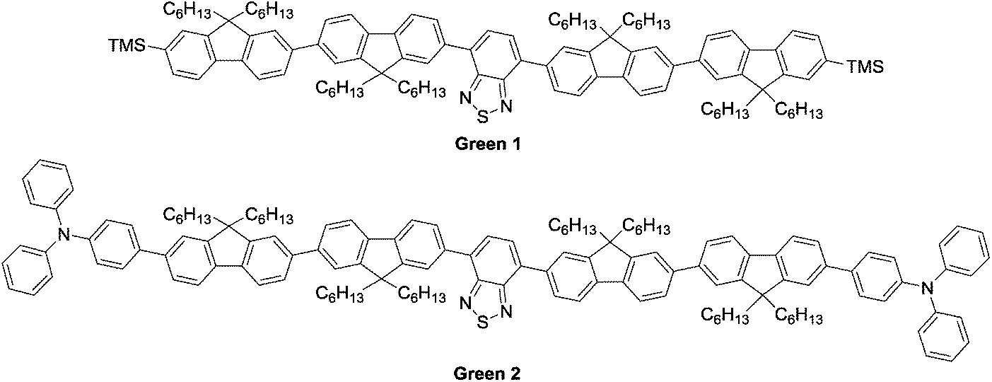
Initially, synthesis of the bifluorene arm (1) component was completed following well-established literature procedures.17 Once in hand, a standard Suzuki–Miyaura coupling between 4,7-dibromobenzothiadiazole 2 and the corresponding boronic acid, using barium hydroxide as base, resulted in isolation of Green 1 in excellent yield as a bright yellow powder. Formation of Green 2 required further manipulation of this structure, first through conversion of the terminal trimethylsilyl groups to bromide, forming intermediate 3, followed by a second Suzuki–Miyaura coupling with 4-(diphenylamino)phenyl boronic acid to form Green 2 in high yield (Scheme 1). Both Green 1 and Green 2 were thermally stable to temperatures greater than 400 °C, and exhibited glass transition temperatures of 65 °C and 91 °C, respectively (see Table 1 and Fig. S1–S4, ESI†). Additionally, Green 2 showed a clear melt transition during heating, which is likely due to the increased opportunity for intermolecular interactions in the extended aromatic system compared with Green 1. Solution state UV-vis absorption and photoluminescence (PL) spectra were recorded as dilute solutions in dichloromethane (Fig. 2 and Table 1). Green 1 showed one absorption band (346 nm) with an additional, less intense absorption at longer wavelength (425 nm), corresponding to a charge transfer band. Similarly, Green 2 revealed an intense band at 365 nm with a lower energy shoulder (420 nm). To determine the wavelength of emission, each molecule was excited at the wavelength corresponding to the most intense absorption. Both Green 1 and Green 2 exhibited a sharp emission profile at 549 and 546 nm, respectively. The cyclic voltammetry (CV) of both Green 1 and Green 2 revealed an almost identical reversible reduction wave for each compound, with very close values for their LUMO levels (Table 1, and Fig. S5–S8, ESI†). The oxidation cycle of Green 1 showed two closely positioned one-electron quasi-reversible oxidation waves at around +0.7 V and +1.0 V. The CV of Green 2 exhibited similar oxidation features, although these shifted slightly to greater potentials at ca. +0.8 V and +1.1 V, respectively. Notably, there was no visible separation of the wave at +0.8 V indicating that both bifluorene arms were oxidised simultaneously, while an additional two-electron reversible wave at ca. +0.4 V, corresponding to the oxidation of the terminal triphenylamine units, was also present. As a result, the HOMO level for Green 2 was −5.07 eV, compared to −5.37 eV for Green 1. Consequently, the electrochemical HOMO–LUMO gap for Green 2 was narrower than that of Green 1, compared with near-identical optical HOMO–LUMO gaps for each compound. Absolute photoluminescence quantum yield (PLQY) values in the solid state for Green 1 and Green 2 were recorded as 90.4% and 73.7%, respectively (Table S1, ESI†). | ||
| Scheme 1 The synthesis of Green 1 and Green 2. | ||
| Name | TGAa (°C) | T g (°C) | λ max (abs) (nm) | λ max (PL) (nm) | Optical HOMO–LUMO gapc (eV) | E pox , (V) | E pred , (V) | HOMOd (eV) | LUMOd (eV) | HOMO–LUMO gapf (eV) |
|---|---|---|---|---|---|---|---|---|---|---|
| a Temperature at which 5% mass loss occurs. b Recorded in CH2Cl2 solution (concentration of 10−5 M for absorption and 10−6 M for PL spectra). c Calculated from the onset of the longest wavelength absorbance edge. d Obtained via cyclic voltammetry using glassy carbon, platinum wire and Ag wire as the working, counter and pseudo-reference electrodes, respectively, with (nBu)4PF6 as the electrolyte in dichloromethane solution (0.1 M) at a scan rate of 100 mV s−1. The data were referenced to the Fc/Fc+ redox couple, which has a HOMO of −4.8 eV. e The peaks shown are anodic/cathodic for oxidation and cathodic/anodic for reduction waves. f Calculated by subtraction of the LUMO from the HOMO. g Melt observed at 129 °C. h The wave consists of two closely positioned one-electron waves. | ||||||||||
| Green 1 | 428 | 65 | 346, 425 | 549 | 2.55 | 0.74/0.63h | −1.93/−1.84 | −5.37 | −3.00 | 2.37 |
| 1.01/0.92 | ||||||||||
| Green 2 | 406 | 91g | 365, 420 | 546 | 2.52 | 0.38/0.32 | −1.93/−1.87 | −5.07 | −2.98 | 2.09 |
| 0.77/0.70 | ||||||||||
| 1.06/0.99 | ||||||||||
 | ||
| Fig. 2 Normalised UV-vis absorbance and photoluminescence for Green 1 and Green 2 recorded in dilute dichloromethane solutions (10−5 and 10−6 M, respectively). | ||
Device fabrication and characterisation
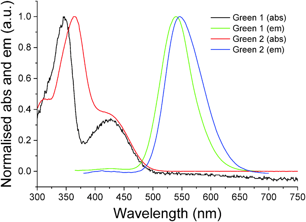
OLED devices of the configuration ITO/PEDOT-PSS/Green 1 (or 2)/Ca/Al were fabricated in order to examine the performance of Green 1 and Green 2 as emissive materials. Fig. 3 shows the electroluminescence spectra and photos of working OLEDs of Green 1 and Green 2. Both OLEDs exhibit a peak at 556 nm and a shoulder at 598 nm. The chromaticity coordinates (x,y) in the Commission Internationale d'Eclairage (CIE) 1931 colour space chromaticity diagram were calculated as (0.42, 0.56) and (0.43, 0.55), respectively. There is also no significant difference in the electroluminescence of Green 1 and Green 2. This was an expected behaviour of these materials from the design perspective since additional charge transport units were added to the structure of Green 2 to improve charge transport characteristics. The basic device architecture used to record the above electroluminescence spectra is shown in Fig. S9 (ESI†). There is a 0.37 eV barrier for hole injection from ITO/PEDOT-PSS to Green 1, but there is an insignificant barrier from ITO/PEDOT-PSS to Green 2. Hence it would be expected that the hole injection from ITO/PEDOT-PSS to Green 2 would be much better than that to Green 1.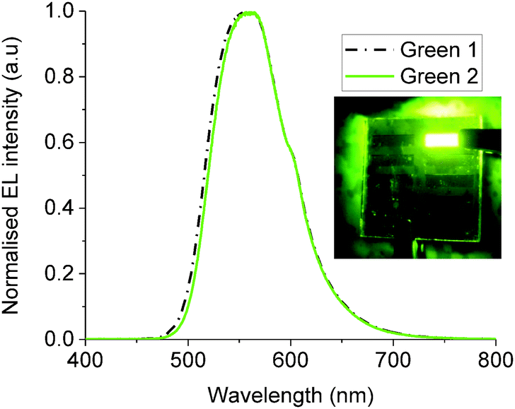 | ||
| Fig. 3 Electroluminescence (EL) spectra of Green 1 and Green 2. Inset shows a working green OLED. | ||
The JVL of unannealed and annealed Green 1 and Green 2 devices are shown in Fig. S11–S14 (ESI†). The unannealed Green 1 device exhibited a highest luminance of 3720 cd m−2 at 10.2 V with a maximum current efficiency of 1.22 cd A−1 at 9.0 V and a maximum external quantum efficiency (EQE) of 0.34%. Green 2 devices exhibited a highest luminance of 15958 cd m−2 at a bias voltage of 9.36 V, with a maximum current efficiency of 1.69 cd A−1 at 7.7 V and a maximum EQE of 0.47%. After achieving these maximum luminance values, both sets of devices experienced a decrease in luminance, which is an expected behaviour in OLEDs due to heating effects.
The JVL of Green 1 and Green 2 devices annealed at 40 °C are shown in Fig. 4. Annealed devices containing Green 1 and Green 2 exhibited maximum luminance intensities of 6724 cd m−2 and 20388 cd m−2, respectively, after treatment at 40 °C. The device characteristics of the annealed devices are shown in Table 2. While Green 2 devices did not show any light output after 80 °C, Green 1 devices exhibited a reduced performance. Both Green 1 and Green 2 devices exhibited higher performances after annealing at 40 °C. There is no significant change in the turn on voltage with Green 2 devices; however, there is a large change in turn-on voltage (4.4 V to 7.0 V) for Green 1 devices after annealing. This 2.6 V difference for Green 1 devices is likely due to morphological changes caused by annealing, resulting in much longer grains as observed in the AFM images shown in Fig. 5 (top). It is reasonable to assume that since the charge carriers have to overcome this unfavourable interface the mobility decreases significantly, which results in a lower probability of recombination in the emissive layer and hence a lower luminance is observed. The shorter, wider grains seen in Fig. 5 (bottom) may provide a favourable interface for charge carrier pathways. Overall, a much lower current is flowing through the Green 1 devices compared to Green 2 emissive layers, which is consistent with the earlier data, suggesting low charge carrier mobility in Green 1.
 | ||
| Fig. 4 Current density–voltage–electroluminescence (JVL) characteristics of Green 1 and Green 2 with device architectures of ITO/PEDOT-PSS/Green/Ca/Al. | ||
| Material | Annealing temperature (°C) | Turn on at 10 cd m−2 (V) | Maximum luminance (cd m−2) | Maximum current efficiency (cd A−1) | Maximum EQE (%) |
|---|---|---|---|---|---|
| Green 1 | Room temperature | 4.43 | 3720@10.2 V | 1.22@9.0 V | 0.34@9.0 V |
| 40 | 6.16 | 6724@9.9 V | 1.74@8.85 V | 0.48@8.85 V | |
| 60 | 6.97 | 4087@11.16 V | 1.49@10.8 V | 0.41@10.8 V | |
| 80 | 6.92 | 504@9.9 V | 1.22@9.0 V | 0.04@9.9 V | |
| Green 2 | Room temperature | 4.18 | 15958@9.36 V |
1.69@7.7 V | 0.47@7.2 V |
| 40 | 4.18 | 20388@8.52 V |
1.71@7.32 V | 0.47@7.9 V | |
| 60 | 4.21 | 17809@9.1 V |
1.7@8.4 V | 0.47@7.7 V | |
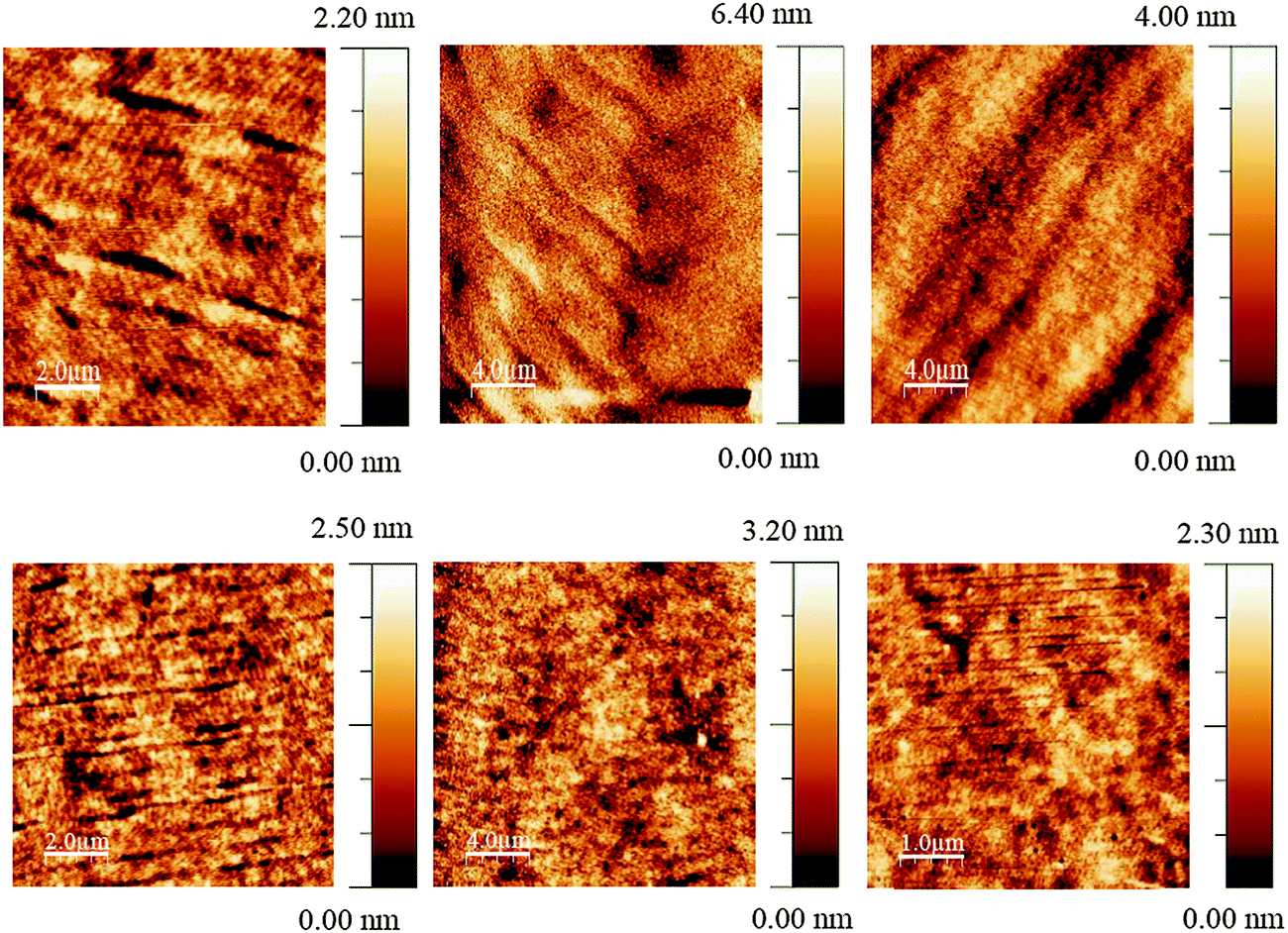 | ||
| Fig. 5 Tapping mode AFM images of optimised Green 1 (top) and Green 2 (bottom) devices at room temperature (left) and annealed at 40 °C (centre) and 80 °C (right). | ||
Due to the higher Tg of Green 2 (91 °C), it is expected that Green 2 did not go through any thermal transitions in the temperature interval used for annealing allowing JVL characteristics to be recorded. However, there are variations in the device characteristics which can be attributed to some morphological re-arrangements over this temperature range, affecting the film morphology and hence charge transport, but are not significantly large enough to be observed in the AFM images.
Since the best characteristics were obtained after annealing the film of the emissive layer at 40 °C, and compared with the device performance without annealing, this slight heat treatment may have created a more favourable morphology that sustains a higher current flow. However, although the device annealed at 80 °C initially carries a large current, it rapidly shorts and no light is emitted. Overall, Green 2 has displayed superior performance characteristics over Green 1 in terms of maximum luminance and current efficiency. Due to the higher Tg, the structure of this material is more stable under heating and less likely to undergo significant, unfavourable morphological changes, within this annealing range.
The J–V characteristics of Green 1 and Green 2 follow strong power law (J ∝ Vm+1) dependence in different operating regions. While slopes (exponent m = 0) under lower voltages can be explained by normal ohmic behaviour, a slope of 2 (exponent m = 1) is attributed to trap filled space charge limited conduction (SCLC). Higher slopes (exponent m > 1) can be explained by bulk limited conductions.18,19 The SCLC in organic semiconductors under the trap filled conditions was given by the Mott–Gurney law. At voltages less than 2.5 V, which is the onset of the turn-on voltage, these devices follow a power law dependence of m = 0. After the turn on point is achieved, all devices follow a power law dependence with m = 4–8, depending on device architecture. Fig. S10 (ESI†) shows a representative logJ vs. logV plot for Green 1 and Green 2 devices with the device architecture of ITO/PEDOT-PSS/Green 1 or 2/Ca/Al. For Green 1 devices the slope of 1.8 before turn-on and a slope of 5.6 after turn on are observed. The corresponding plot for Green 2 devices exhibits three slope values of 1.28, 2.2 and 5.2. A detailed examination of temperature dependence of the exponent m > 1 will identify a dominant charge transport mechanism present in these materials, which is beyond the scope of this work.
The electron-transport layer Alq3 was added to devices containing Green 1 and Green 2. These devices have the device architecture of ITO/PEDOT-PSS/Green 1 or 2/Alq3/Ca/Al. The energy level diagram is shown in Fig. S9 (ESI†), whilst the JVL and current efficiency characteristics of these devices are shown in Fig. S15 and S16 (ESI†). Green 1 devices turned on at 9.3 V, with a maximum luminance of 4702 cd m−2 at 14 V, a current efficiency of 1.11 cd A−1 at 12.18 V and a maximum EQE of 0.31% (Table S2, ESI†). Addition of Alq3 to the Green 1 device architecture did not provide an increase in any of the device characteristics, but resulted in a lower overall performance. Green 2 devices turned on at 5.9 V and afforded a highest luminance of 17189 cd m−2 at 11.9 V, with a maximum current efficiency of 3.47 cd A−1 at 10.6 V and maximum EQE of 0.92%. The recorded operating voltages and an increase in turn on voltages of Green 1 and Green 2 devices after the addition of Alq3 can be attributed to the increased thickness of the devices. Although there is a slight decrease in the maximum luminance of Green 2 devices containing Alq3 as an ETL layer compared to that of the reference devices, the current efficiency increases to 3.47 cd A−1 (at 10.68 V) from 1.71 cd A−1 (at 7.32 V) of the reference devices.
Experimental
General experimental
Tetrakis(triphenylphosphine)palladium(0) (Pd(PPh3)4) was prepared prior to use and stored under nitrogen. Unless otherwise stated, all other reagents were sourced commercially and used without further purification. Dry solvents were obtained from a solvent purification system (SPS 400 from Innovative Technologies) using alumina as the drying agent. 1H and 13C NMR spectra were recorded on either a Bruker DRX 500 apparatus at 500.13 and 125.76 MHz, or a Bruker Avance DPX400 apparatus at 400.13 and 100.6 MHz. Chemical shifts are given in ppm; all J values are in Hz. Elemental analyses were obtained on a Perkin-Elmer 2400 analyser. MS LDI-TOF spectra were run on a Shimadzu Axima-CFR spectrometer (mass range 1–150000 Da). Thermogravimetric analysis (TGA) was performed using a Perkin-Elmer thermogravimetric analyser TGA7 under a constant flow of helium. Melting points were taken using a TA instruments DSC QC1000 Differential Scanning Calorimeter.
Cyclic voltammetry (CV) measurements were performed on a CH Instruments 660A electrochemical workstation with iR compensation using anhydrous dichloromethane as the solvent. The electrodes were glassy carbon, platinum wire and silver wire as the working, counter and reference electrodes, respectively. All solutions were degassed (Ar) and contained monomer substrates in concentrations of ca. 10−4 M, together with n-Bu4NPF6 (0.1 M) as the supporting electrolyte. All measurements are referenced against the E1/2 of the Fc/Fc+ redox couple. Absorption spectra were recorded on a Shimadzu UV 2700 instrument. Photoluminescence measurements were recorded using a Perkin-Elmer LS 50 B fluorescence spectrometer in a quartz cuvette (path length 10 mm). Absolute PLQY measurements were recorded in a calibrated integrating sphere attached to an Ocean Optics USB2000 + spectrometer and a Gooch & Housego double monochromator with a quartz halogen lamp. The samples were excited at 346 and 365 nm, respectively.
Device fabrication
Pre-patterned ITO slides were cleaned with organic solvents in an ultrasonic bath followed by oxygen plasma cleaning. High conductivity PEDOT:PSS (Heraus AL 4083) was spin-coated onto the pre-cleaned ITO substrates and annealed at 120 °C for about 20 minutes and then cooled to room temperature. These substrates were transferred into a glove box where all the subsequent fabrications and measurements were performed. Green 1 and Green 2 solutions were prepared by using toluene with varying concentrations of 10, 20 and 30 mg ml−1. A solution concentration of 20 mg ml−1 was found to be optimum and hence used to continue other characterisation measurements such as annealing. These spin-coated films were annealed for 20 minutes at temperatures of 40, 60 and 80 °C. After annealing these films were transferred into a thermal evaporator attached to the glove box for evaporation of the electrodes. An active area of 1.5 × 4 mm2 was obtained by evaporation of 40 nm of calcium and 40 nm of aluminium electrodes through a shadow mask at the base pressure of 1 × 10⁻⁶ mbar. A Dimension 3100 Atomic Force Microscope was used to analyse surfaces of these films under tapping mode. JVL were measured inside the glove box with a light-tight box attached. A Keithley Semiconductor Characterisation (SCS) 4200 was used to bias the OLEDs. Luminance measurements were performed by using a Macom L203 photometer with a calibrated silicon photodetector and a photopic filter. These calibrations can be traced back to the National Physical Laboratory, London standards. Wavelength dependent electroluminescence spectra were measured by using an Ocean optics USB2000 + spectrometer under a lab atmosphere.Green 1
Compound 1 (852 mg, 1.09 mmol, 3.2 eq.), 4,7-dibromo-2,1,3-benzothiadiazole 2 (100 mg, 0.34 mmol, 1.0 eq.), tetrakis(triphenylphosphine)palladium(0) (81 mg, 0.07 mmol, 0.2 eq.) and barium hydroxide hydrate (515 mg, 1.63 mmol, 4.8 eq.) were charged to a reaction flask, evacuated, and purged with Ar (×3). Anhydrous THF (15 ml) was then added, followed by degassed, deionised water (1.03 ml), and the reaction mixture heated to reflux for 48 h. After this time, the reaction mixture was cooled to room temperature and quenched by addition of water (100 ml). The organic residues were extracted with dichloromethane (4 × 50 ml) and all the organic layers combined, before being dried over MgSO4, filtered and concentrated to a green residue. Purification on silica gel, eluting with 10–15% dichloromethane in hexane afforded a bright orange solid. This residue was dissolved in the minimum volume of hot dichloromethane and precipitated with cold methanol, with rapid cooling in a cold bath at −80 °C used to achieve precipitation. Filtration and drying under vacuum afforded the title compound as an orange powder (509 mg, 93%); δH (CDCl3, 500.13 MHz) 8.08 (2H, dd, J 7.5, 1.5, ArH), 8.02 (2H, s, ArH), 7.95–7.92 (4H, m, ArH), 7.87 (2H, d, J 7.5, ArH), 7.82 (2H, d, J 8.0, ArH), 7.75–7.66 (10H, m, ArH), 7.54–7.52 (4H, m, ArH), 2.16–2.05 (16H, m, CH2), 1.20–1.12 (48H, m, CH2), 0.92–0.80 (40H, m, CH2, CH3), 0.33 (18H, s, CH3Si); δC (CDCl3, 125.76 MHz) 154.4, 152.1, 151.7, 151.4, 150.2, 141.4, 141.1, 140.9, 140.6, 140.4, 139.8, 139.0, 136.2, 133.6, 131.9, 128.3, 127.9, 127.7, 126.2, 126.1, 124.0, 121.6, 120.2, 120.0, 119.8, 119.0, 55.4, 55.1, 40.3, 40.1, 31.5, 31.4, 29.7, 29.6, 24.0, 23.7, 22.6, 22.5, 14.04, 14.01, −0.8; m/z (MALDI-TOF) 1609.5; anal. calculated for C112H148N2SSi2: C, 83.52; H, 9.26; N, 1.74%. Found: C, 83.37; H, 9.39; N, 1.74%; TGA: 5% mass loss at 428 °C; Tg = 64.89 °C.Compound 3
Green 1 (400 mg, 0.248 mmol, 1.0 eq.) and sodium acetate (41 mg, 0.496 mmol, 2.0 eq.) were charged to a reaction flask, evacuated and purged with Ar (×3). Anhydrous THF (10 ml) was added, and the mixture cooled to 0 °C. Bromine (184 mg, 1.156 mmol, 4.66 eq., in dichloromethane (0.42 ml)) was added and the mixture stirred at 0 °C covered in foil. After 1 h, analysis by 1H NMR indicated complete reaction. Triethylamine (0.32 ml, 2.31 mmol, 9.32 eq.) and sodium sulphite (sat., 100 ml) were added to quench the reaction, and the mixture extracted with dichloromethane (3 × 50 ml). The combined dichloromethane extracts were washed with sodium bicarbonate (sat., 100 ml), dried (MgSO4) and concentrated. The residue was loaded onto silica gel and filtered through a short silica plug, eluting with dichloromethane/hexane (1:1). Concentration of the appropriate fractions afforded an orange solid that was used in the next step without further purification (399 mg, 99%); δH (CDCl3, 400.13 MHz) 8.07 (2H, dd, J 7.6, 1.6, ArH), 8.01 (2H, s, ArH), 7.94–7.92 (4H, m, ArH), 7.87 (2H, d, J 8.0, ArH), 7.7 (2H, d, J 8.0, ArH), 7.70–7.60 (10H, m, ArH), 7.50–7.48 (4H, m, ArH), 2.16–1.98 (16H, m, CH2), 1.18–1.10 (48H, m, CH2), 0.89–0.81 (40H, m, CH2, CH3).
Green 2
Compound 3 (399 mg, 0.246 mmol, 1.0 eq.), 4-(diphenylamino)phenyl boronic acid (227 mg, 0.786 mmol, 3.2 eq.), tetrakis(triphenylphospine)palladium(0) (57 mg, 0.049 mmol, 0.2 eq.) and barium hydroxide hydrate (373 mg, 1.18 mmol, 4.8 eq.) were charged to a reaction flask, evacuated and purged with Ar (×3). Anhydrous THF (15 ml) and degassed, distilled water (0.75 ml) were added and the mixture heated to reflux for 20 h. The mixture was then cooled, diluted with water (100 ml), then extracted with dichloromethane (3 × 60 ml). The combined organic extracts were dried (MgSO4) and concentrated under vacuum to a dark orange residue. Silica gel column chromatography, eluting with 20% dichloromethane/hexane, afforded the product as a bright orange residue that was dissolved in the minimum volume of hot dichloromethane and precipitated with ice cold methanol. Further cooling in liq. N2 afforded an orange powder that was isolated by filtration. The product was hence isolated as bright orange powder (409 mg, 85%); δH (CDCl3, 500.13 MHz) 8.08 (2H, dd, J 8.0, 1.6, ArH), 8.02 (2H, s, ArH), 7.94–7.92 (4H, m, ArH), 7.87 (2H, d, J 7.6, ArH), 7.83–7.78 (4H, m, ArH), 7.72–7.66 (8H, m, ArH), 7.60–7.58 (8H, m, ArH), 7.32–7.27 (8H, m, ArH), 7.21–7.16 (12H, m, ArH), 7.08–7.04 (4H, m, ArH), 2.15–2.08 (16H, m, CH2), 1.17–1.10 (48H, m, CH2), 0.90–0.76 (40H, m, CH2, CH3); δC (CDCl3, 125.76 MHz) 151.7, 147.7, 129.3, 127.8, 124.4, 124.1, 122.9, 120.0, 55.4, 55.3, 40.5, 40.3, 31.5, 29.8, 24.0, 23.8, 22.6, 14.0; m/z (MALDI-TOF) 1952.1; anal. calculated for C142H158N4S: C, 87.33; H, 8.16; N, 2.87%. Found: C, 87.61; H, 8.24; N, 3.20%; TGA: 5% mass loss at 406 °C; Tg = 91.14 °C, Tm = 117.69 °C, Tc = 127.64 °C.Conclusions
Two novel, linear small molecules containing an electron-deficient benzothiadiazole core and electron-rich bifluorene arms have been prepared and their performance as emissive components in solution-processed OLEDs examined. Both molecules produce green light, with a maximum electroluminescence in excess of 20000 cd m−2, realised using Green 2.
Acknowledgements
The authors thank the Korean Institute for the Advancement of Technology (KIAT) and the EPSRC for funding (EP/I029141 and EP/K00042X). Additionally, PJS thanks the Royal Society for a Wolfson Research Merit Award.Notes and references
- C. J. Humphreys, MRS Bull., 2008, 33, 459 CrossRef.
- R. Haitz and J. Y. Tsao, Phys. Status Solidi A, 2011, 208, 17 CrossRef CAS.
- A. C. Grimsdale, K. L. Chan, R. E. Martin, P. G. Jokisz and A. B. Holmes, Chem. Rev., 2009, 109, 897 CrossRef CAS PubMed.
- L. Duan, L. Hou, T.-W. Lee, J. Qiao, D. Zhang, G. Dong, L. Wang and Y. Qiu, J. Mater. Chem., 2010, 20, 6392 RSC.
- A. L. Kanibolotsky, I. F. Perepichka and P. J. Skabara, Chem. Soc. Rev., 2010, 39, 2695 RSC.
- L. Ying, C.-L. Ho, H. Wu, Y. Cao and W.-Y. Wong, Adv. Mater., 2014, 26, 2459 CrossRef CAS PubMed.
- X.-H. Zhu, J. Peng, Y. Caoa and J. Roncali, Chem. Soc. Rev., 2011, 40, 3509 RSC.
- T. M. Eggenhuisen, Y. Galagan, A. F. K. V. Biezemans, T. M. W. L. Slaats, W. P. Voorthuijzen, S. Kommeren, S. Shanmugam, J. P. Teunissen, A. Hadipour, W. J. H. Verhees, S. C. Veenstra, M. J. J. Coenen, J. Gilot, R. Andriessen and W. A. Groen, J. Mater. Chem. A, 2015, 3, 7255 CAS.
- T. M. Eggenhuisen, Y. Galagan, E. W. C. Coenen, W. P. Voorthuijzen, M. W. L. Slaats, S. A. Kommeren, S. Shanmuganam, M. J. J. Coenen, R. Andriessen and W. A. Groen, Sol. Energy Mater., 2015, 134, 364 CrossRef CAS.
- T.-W. Lee, T. Noh, H.-W. Shin, O. Kwon, J.-J. Park, B.-K. Choi, M.-S. Kim, D. W. Shin and Y.-R. Kim, Adv. Funct. Mater., 2009, 19, 1625 CrossRef CAS.
- J. H. Burroughes, D. D. C. Bradley, A. R. Brown, R. N. Marks, K. Mackay, R. H. Friend, P. L. Burn and A. B. Holmes, Nature, 1990, 347, 539 CrossRef CAS.
- L. S. Liao and K. P. Klubek, Appl. Phys. Lett., 2008, 92, 223311 CrossRef.
- S.-Y. Ku, L.-C. Chi, W.-Y. Hung, S.-W. Yang, T.-C. Tsai, K.-T. Wong, Y.-H. Chen and C.-I. Wu, J. Mater. Chem., 2009, 19, 773 RSC.
- Z. Zhao, S. Chen, J. W. Y. Lam, Z. Wang, P. Lu, F. Mahtab, H. H. Y. Sung, I. D. Williams, Y. Ma, H. S. Kwok and B. Z. Tang, J. Mater. Chem., 2011, 21, 7210 RSC.
- P. Moonsin, N. Prachumrak, S. Namuangruk, S. Jungsuttiwong, T. Keawin, T. Sudyoadsuk and V. Promarak, Chem. Commun., 2013, 49, 6388 RSC.
- Y. Li, A.-Y. Li, B.-X. Li, J. Huang, L. Zhao, B.-Z. Wang, J.-W. Li, X.-H. Zhu, J. Peng, Y. Cao, D.-G. Ma and J. Roncali, Org. Lett., 2009, 11, 5318 CrossRef CAS PubMed.
- C. R. Belton, A. L. Kanibolotsky, J. Kirkpatrick, C. Orofino, S. E. T. Elmasly, P. N. Stavrinou, P. J. Skabara and D. D. C. Bradley, Adv. Funct. Mater., 2013, 23, 2792 CrossRef CAS.
- W. Bruetting, S. Berleb and A. G. Mueckl, Org. Electron., 2001, 2, 1 CrossRef.
- A. J. Campbell, M. S. Weaver, D. G. Lidzey and D. D. C. Bradley, J. Appl. Phys., 1998, 84, 6737 CrossRef CAS.
Footnote |
| † Electronic supplementary information (ESI) available: Thermal analysis, cyclic voltammetry, energy level diagram for organic components, additional device data. See DOI: 10.1039/c5tc03579a |
| This journal is © The Royal Society of Chemistry 2016 |