
 Open Access Article
 This Open Access Article is licensed under a
 Creative Commons Attribution 3.0 Unported Licence
Ammonia sensing for enzymatic urea detection using organic field effect transistors and a semipermeable membrane†
F. X.
Werkmeister
a,
T.
Koide
ab and
B. A.
Nickel
*ac
aFakultät für Physik & CeNS, Ludwig-Maximilians – Universität München, München, D-80539, Germany. E-mail: nickel@lmu.de
bJapan Patent Office, 3-4-3 Kasumigaseki, Chiyoda-ku, Tokyo 100-8915, Japan
cNanosystems Initiative Munich (NIM), D-80799 Munich, Germany
First published on 17th November 2015
Abstract
Organic Field Effect Transistors (OFETs) are used to measure ammonia in solution via ammonia diffusion into the OFET channel. An increase in ammonia concentrations results in a decrease in transistor currents. The regeneration of the OFET current after ammonia uptake is slow, which allows us to read out the maximum ammonia dose which was applied. A 100 nm parylene-C layer serves as a semipermeable top gate dielectric. The parylene layer is functionalized with the covalently attached enzyme urease. The enzyme catalyses the hydrolysis of urea to ammonia and carbon dioxide, i.e. urea can be detected via its hydrolysis product ammonia. The sensitivity covers a range of physiological concentrations of urea, which are several mM.
Introduction
Ammonia, the end product of amino acid metabolism, is highly toxic. Therefore, ammonia is circulated only in low concentrations in body fluids, and most of it is first converted into urea in a cycle of biochemical reactions known as the urea cycle. Urea is present in body fluids in high concentrations; in healthy humans, the normal range of urea concentrations in blood is 2.5–7 mM.1 The measurement of urea concentrations is important as a marker for e.g. potential kidney malfunction.2,3 Specific detection of urea is possible by the enzyme urease. Urease catalyzes the hydrolysis of urea to ammonium (NH4+) and carbon dioxide in water: | (1) |
 | (2) |
For enzymatic urea detection via its hydrolysis product ammonium and OH− (eqn (1)), one could consider a pH based or ion specific detection scheme.4,23 Here, a shift of the electrochemical potential due to urea hydrolysis is picked up via a shift in the electrostatic gate potential, which controls the semiconducting channel.4 This approach is limited for a weak base as ammonium since ammonium forms in solution a chemical equilibrium between NH4+ and ammonia (NH3):
| NH4+ + H2O ↔ NH3 + H3O+ | (3) |
Note that another reaction product of the hydrolysis (eqn (1)) is CO2. CO2, however, is known to have only negligible interactions with organic transistors,36 and thus not expected to influence device characteristics. It can form a chemical equilibrium with carbonic acid and thus contribute to buffering in solution.
Here, we explore OFETs for the detection of urea. For this purpose, we fabricated a 100 nm parylene-C membrane onto the OFETs and functionalized the parylene-C surface with a covalently attached enzyme, urease. We suggest that urea can be detected via its hydrolysis product ammonia. Ammonia should be able to diffuse through the parylene-C membrane and give rise to a response via trapping of charge carriers in the organic semiconductor film. To determine the mechanism of sensing, i.e. pH vs. trapping, the response of the OFETs towards shifts of the pH value as well as NH3 concentration in solution is tested, with a detailed investigation of the latter. Finally, the urea concentration range, which can be detected, is determined.
Experimental
OFET fabrication
Glass slides (R. Langenbrinck) were cleaned in an ultrasonic bath with acetone, 2-propanol, and Milli-Q water for 10 min each. Next nominally 1.7 μm parylene-C (Plasma Parylene Systems GmbH) was deposited in a homebuilt CVD chamber via the Gorham route. Source and drain electrodes were defined from 20 nm of Au using a Lift-Off process: a bilayer of LOR 3B and S1813 G2 was spin coated, illuminated and developed using Microposit 351 Developer. The LOR 3B layer beneath the photoresist gives rise to an undercut in the dual layer during development and avoids fencing at the rims of the patterned metal electrodes after Lift-Off. Lift-Off was performed with 1165 Remover. The electric leads defined on the surface were encapsulated with a layer of SU 8 (Microchem), which was processed as recommended by the fabricant; mr-Dev 600 (Microchemicals GmbH) was used as a developer. 18 nm DNTT (Sigma 767638, purified by one sublimation run by CreaPhys GmbH) was deposited thermally onto the transistor areas through a shadow mask at a rate of 0.2 Å s−1 with the substrates at room temperature and a base pressure of <10−6 mbar. The devices were encapsulated by depositing ca. 100 nm parylene-C onto the transistor area. The area of parylene-C deposition was defined by a PDMS mask put onto the devices.Surface treatment and urease attachment
The OFETs were treated with oxygen plasma in a plasma cleaner (50 W power, 2 mbar, 18 s). Immediately afterwards, the OFETs were put into a 1 vol% aqueous solution of APTES (Sigma A3648) for at least 4 h. Subsequently, the OFETs were dried under gentle nitrogen flow and put into a 5% solution of glutaraldehyde (Sigma G6257) for at least 4 hours. After drying under nitrogen flow again, the urease was bound to the surface by putting the OFETs into a solution of urease (Sigma U1500, 75 mg) in PBS buffer (10 mM, 15 ml).Assembly into the flow chamber
Commercially available sticky slides IV 0.4 (Ibidi GmbH) were modified as follows: the adhesive tape was peeled off from the flow chamber and the holes necessary for the electrical contacts were drilled utilizing a CNC milling machine. After drilling the holes 467 MP adhesive tape (3 M) was applied to the bottom of the slides and patterned according to the holes and the channel. A PtIr (Pt80/Ir20, GoodFellow, PT045110) wire was introduced into each channel after being glowed out using a Bunsen burner to serve as the electrode in the electrolyte. Finally, the OFET was attached to the modified sticky slides and the glue was given one night to obtain a good seal.Electrical measurements
Measurements were performed using a linked system of a Keithley 2612 and 2602 source measurement unit. The source and drain contacts were hot switched using a Keithley 7072 switching matrix card. The equipment was controlled using custom written LabView programs. The potential in the electrolyte (top gate) was swept down to −0.6 V versus the source contact. The source drain bias was −0.3 V versus the source. All measurements were performed in ambient at 20–21 °C.pH measurements in the electrolyte
The solution for any measurement was based on 10 mM Dulbecco's phosphate buffered saline solution without Ca/Mg (Biochrom L 182-50, powder dissolved in Milli-Q water). Urea (Sigma U0631) and ammonia (Carl Roth 5460.1) were dissolved/pipetted into 10 mM DPBS solution. A HANNA 213 pH meter was used for the pH measurements and calibrated before each use.AFM measurements
AFM micrographs were recorded using a Veeco Dimension 3100 AFM in tapping mode. The software Gwyddion 2.40 was used for evaluation.Results and discussion
We designed an OFET gated via a Pt/Ir wire in solution (Fig. 1a). A parylene-C layer with source and drain electrodes patterned by photolithography for bottom contact served as a substrate.37 Dinaphtho[2,3-b:2′,3′-f]thieno[3,2-b]thiophene (DNTT) was chosen as the organic semiconductor for its stability38 and thermally deposited onto the substrate to form the organic semiconducting channel (Fig. 1b). Onto the semiconductor channel, we deposited a 100 nm thick parylene-C layer, which served as the top gate dielectric (ESI†). Furthermore, parylene-C dielectric's surface can be functionalized by a silane coupling reaction. The functionalization procedure was based on a silane coupling reaction adapted from the functionalization of silicon dioxide dielectrics of inorganic silicon biosensors.4 To activate the parylene-C surface, it was treated with an oxygen plasma for 18 s.39 Here, the stability of DNTT versus oxidation was necessary to maintain transistor operation after the oxygen treatment. Less stable organic semiconductors might be employable, if parylene derivatives are employed, which facilitate functionalization procedures avoiding plasma activation.40 Oxygen plasma treated parylene-C surfaces were silanized by 3-aminopropyltriethoxysilane (APTES). Subsequently, glutaraldehyde and urease were bound to this surface. To verify the function of bound urease, the catalysis of urea was tested. Urea was dissolved in Milli-Q water to a concentration of 10 mM. This solution was added into a beaker together with dissolved urease or a treated parylene-C surface on glass. The pH value of the solution was measured against the time using a digital pH meter (ESI,† Fig. S5). The maximum value of pH attainable was 9.3, likely the urease degraded at this pH value. For the lower amount of urease, the pH value saturated at decreasing values. This implied a limited total number of catalyses sustainable for an individual urease enzyme. We found that the pH response for the bound urease was comparable to a concentration above 10 μg ml−1 of free urease in solution, albeit slower. The slower response of bound urease is likely due to mass transport from and to the surface and a larger distance of the pH meter from the reaction. | ||
| Fig. 1 (a) Schematic of the OFET device architecture and measurement scheme in solution. (b) AFM micrograph of the DNTT film in an OFET channel of length 5 μm. The source–drain electrodes are visible to the left and the right. (c) pH effect on the transconductance curve of an OFET. | ||
First, we tested the pH response of our OFET. The pH value of 10 mM Dulbecco's phosphate buffered saline (DPBS) solution was adjusted by HCl and NaOH. Increasing the pH value from 7.5 to 8.5 results in a positive threshold voltage shift (Fig. 1c). This shift exceeds the Nernstian limit for a single type of charged surface group.41 Most likely, the enzyme layer is responsible for this behavior. A further increase of the pH values from 8.45 to 9.3 and above results in small threshold voltage shifts only. Likely, the enzyme degraded (see S5, ESI†) and the functionalization layer covering the transistor changed its properties. Similarly, the small increase in transconductance observed with increasing pH value may result from conformational changes of the urease layer. Consequently, we conclude that the bound enzyme layer is responsible for the observed pH response, which gives rise to an overall increase of transistor current with increasing pH.
Second, we tested the response and sensitivity of our OFET towards ammonia in solution. Ammonia was dissolved in DPBS solution with concentrations of 0.1 mM, 1 mM and 10 mM. For 0.1 mM solution, no change was observed, see Fig. 2a, red circles and black squares, while for a 1 mM solution, a small change was observed (Fig. 2a, blue triangles). For an ammonia concentration of 10 mM, the transistor current reduced to half of the initial value in a matter of tens of seconds (Fig. 2b). This is encouraging, because the ammonia concentrations that cause this strong response are comparable to the relevant urea concentrations in body fluids of 2.5 to 7 mM.1
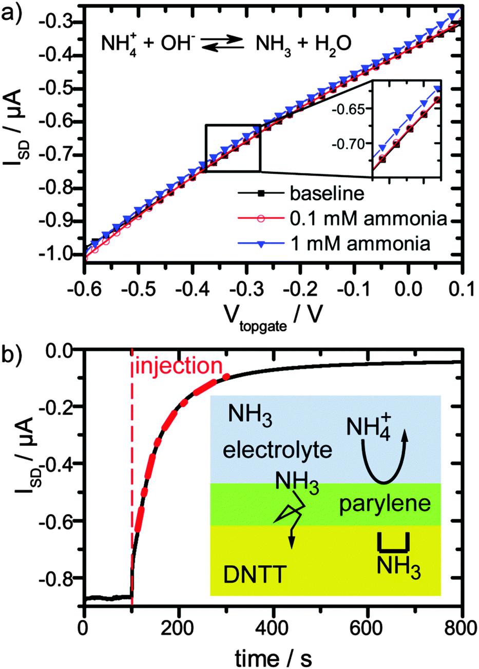 | ||
| Fig. 2 (a) Effect of small ammonia concentrations (0 mM, 0.1 mM, and 1 mM) in 10 mM DPBS buffer on the transconductance, shown as black, red, and blue curves, respectively. (b) Time resolved OFET current upon addition of 10 mM ammonia solution with Vtopgate = −0.4 V. The scheme shows the proposed interaction mechanism of ammonia with the organic semiconductor. All data were recorded at VSD = −0.3 V. | ||
Remarkably, the reduction of current with increasing ammonia and pH is opposite to the pure pH effect. This suggests that the current reduction dominated from NH3 passing the encapsulation layer and diffusing into the semiconductor. In order to quantify this argument, we estimate the amount of NH3 for a 1 mM ammonia solution at the pH of 7.75 and for a 10 mM solution at a pH of 10.17. The ratio of NH3 and NH4+ depending on the pH is given by the Henderson–Hasselbach equation:
 | (4) |
 | ||
| Fig. 3 pH value and ratio of NH3vs. NH4+ depending on ammonia concentration in 10 mM DPBS. The ratio was calculated assuming a Ka of ammonia of 9.6, since the literature value of 9.442 for ammonia in water leads to unphysical results. | ||
We find that the NH3 concentration is increased by a factor of ca. 1000 between ammonia concentrations of 1 and 10 mM, which suggest that indeed NH3 causes the transistor current drop. In fact, detection of ammonia in solution, as demonstrated here, is interesting itself, because it is an indicator of a range of diseases.43
The device response towards an increase of ammonia concentration occurs within seconds (Fig. 2b). Since our analysis suggested that the diffusion of NH3 into the semiconductor layer dominates the response, we assume that the NH3 profile is described by a 1D solution of Fick's 2nd law of diffusion:19
 | (5) |
While parylene is apparently no diffusion barrier for neutral NH3, it is very efficient in suppressing diffusion of charged ions (Na+ and Cl−) to the channel region. This is because the movement of an ion (with radius a and valency Z) from water into an nonpolar medium with dielectric constant ε is prohibited by a high energy barrier, the Born charging energy (Ze)2/8πε0εa.46 This effect gives rise to the high resistance of lipid bilayers.47 This principle also applies to the case of an nonpolar organic semiconductor (ε ≈ 80 for water46 and ε ≈ 3 for pentacene14) or nonpolar encapsulation layers such as parylene. In practice, defects, e.g. pores, in nonpolar layers can lower the energy barrier,46 thus materials and processing have to be carefully chosen.10,48 In summary, the parylene acts here as a semipermeable membrane which blocks ions, while charge neutral NH3 molecules pass through rapidly. Diffusion speed in parylene decreases with the molecule size,49 therefore larger molecules will also be blocked.
Upon rinsing with fresh DPBS buffer after application of 10 mM ammonia solution, the current of the transistor recovers slowly (ESI,† Fig. S6). Apparently, the process of loading NH3 into the semiconducting layer was much faster than the unloading process. This is reasonable, since the NH3 gradient driving the diffusion from 10 mM ammonia solution to the pristine semiconducting film is much steeper than the one from the NH3 loaded semiconducting film to the bare DPBS solution. Additionally, during exposure to the ammonia solution, ammonia may pass the semiconducting layer and diffuse into the parylene layer beneath the organic semiconductor. Subsequent release would take place via diffusion through the organic semiconductor with a very low rate, i.e. the parylene layer beneath the organic semiconductor acts as a reservoir.
Finally, the urea sensing of OFETs with bound urease was evaluated. Different concentrations of DPBS solutions with urea were prepared and pipetted into the flow channel of the sensor after completion of the first gate sweep. Gate sweeps were recorded continuously and the change of the transconductance curve after fixed time (5 min) was evaluated (Fig. 4, red data points). The first response was detected for a urea concentration of 0.75 mM. Between the different urea concentrations, we rinsed the flow channel with fresh DPBS buffer by replacing the complete liquid volume 5 times with fresh buffer. Due to the slow recovery, the transistor current stayed at the low level (Fig. 4, gray data points) suggesting that the device is best suited to monitor the maximal dose that the semiconductor film has seen. We observed a systematic decrease of the current up to a urea concentration of 7.5 mM, i.e. the device covers the full urea range in a healthy patient. In comparing the response in Fig. 4 to the ammonia concentration dependence in Fig. 3 one may note that the response starts before the pronounced increase in NH3 in Fig. 3. Already below the pronounced increase in NH3 at 2 mM in Fig. 3 the NH3 concentration is nonzero and linearly increasing. Organic transistors are sensitive to small amounts of NH3,29,50 as also observed here in the detection of 1 mM ammonia (Fig. 2a). Furthermore, the response of organic transistors with increasing NH3 tends to saturate,50 which is also seen here for higher urea/ammonia concentrations (Fig. 4). After some measurement cycles, our OFETs did not react any more to the addition of urea, even after long times of regeneration. This is not unexpected, since urease was expected to sustain only a limited number of reactions before degradation. Hence, the device is best used as a disposable (use once) sensor, very much in agreement with what is needed in typical healthcare applications.
 | ||
| Fig. 4 Influence of increasing urea concentrations on transistor current. The first source–drain current ISD at VSD = −0.3 V and Vtopgate = −0.3 V (without urea) is used as reference current I0 (grey data point). The resultant ratio ISD/I0 (red dots) is displayed as recorded after 5 min exposure to a given urea concentration. After each exposure, and prior to the next exposure the OFETs are rinsed with fresh buffer by exchanging the liquid volume 5 times. The ratio ISD/I0 prior to each urea exposure is shown after rinsing with buffer as grey squares. The data points are an average of the data of 3 different OFETs with the error bars giving the standard deviation. | ||
Now, we compare the sensitivity of our device with other detection schemes. In electrochemical detection, the reaction is coupled to a redox species and the corresponding charge transfer is recorded. This way a detection range of 0.8–16.6 mM could be realized.51 Another transduction mechanism is to record the potential shift of a pH sensitive device due to the change of the pH value by the hydrolysis of urea in solution.4 A detection range of 0.05–10 mM was reported for urease functionalized polymer membranes coupled to an external FET.52 Both schemes used Ag/AgCl reference electrodes, which are hard to miniaturize53 and integrate into fabrication schemes. Here, we propose a detection scheme, which covers the urea range of medical samples. Our detection scheme relies on NH3 concentration. Since the NH3 interaction dominates electrochemical effects, it is less affected by potential changes. This makes it possible to use a simple Pt/Ir wire as a gate electrode in the electrolyte. A Pt electrode13 can be included as a planar electrode on top of the device during fabrication of the OFET.
Conclusions
In conclusion, we demonstrated an OFET configuration, which allows the measurement of NH3 in aqueous solution. The OFET shows a rapid current decrease within seconds due to the diffusion of NH3 through a semipermeable parylene membrane into the organic semiconducting layer. Therefore, in applications where organic electronic devices are to work in a biological environment, undesired influences of NH3 should be taken into account. Furthermore, such OFETs can detect physiologically relevant urea concentrations of 0.75 mM to 7.5 mM due to urea hydrolysis into NH3 by anchoring urease to the membrane. Regeneration of transistor current is slow, thus the device is well suited for the readout of the maximal urea dose that the device has been exposed to. In turn, the readout may be performed after exposure to e.g. body fluids, which may be interesting for diagnosis purposes. We expect that OFETs with thin and micro-/nanopatterned organic semiconductor layers will show improved sensitivity as well as faster response and recovery times. This case study shows that gas sensing of partial pressure32 and sensing of molar concentration in solution are similar. In liquid, a non-polar semipermeable membrane allows us to separate neutral molecules from the charged species and stabilizes the device. This opens up interesting avenues for design of biosensors utilizing organic semiconductors.Acknowledgements
We would like to thank Prof. Kersting (LMU & CeNS) for providing access to the parylene coater. We acknowledge funding from the Deutsche Forschungsgemeinschaft (DFG) through the Sonderforschungsbereich SFB 1032 “Nanoagents” project A07. Teru Koide would like to thank the Japan patent office for the opportunity of his research stay at the LMU.References
- I. Gotsman, D. Zwas, D. Planer, D. Admon, C. Lotan and A. Keren, Medicine, 2010, 89, 197–203 CrossRef CAS PubMed.
- M. Singh, N. Verma, A. K. Garg and N. Redhu, Sens. Actuators, B, 2008, 134, 345–351 CrossRef CAS.
- G. Dhawan, G. Sumana and B. D. Malhotra, Biochem. Eng. J., 2009, 44, 42–52 CrossRef CAS.
- D. Niwa, K. Omichi, N. Motohashi, T. Homma and T. Osaka, Sens. Actuators, B, 2005, 108, 721–726 CrossRef CAS.
- A. Poghossian and M. J. Schöning, Electroanalysis, 2014, 26, 1197–1213 CrossRef CAS.
- D. Khodagholy, J. Rivnay, M. Sessolo, M. Gurfinkel, P. Leleux, L. H. Jimison, E. Stavrinidou, T. Herve, S. Sanaur, R. M. Owens and G. G. Malliaras, Nat. Commun., 2013, 4, 2133 Search PubMed.
- P. Leleux, C. Johnson, X. Strakosas, J. Rivnay, T. Hervé, R. M. Owens and G. G. Malliaras, Adv. Healthcare Mater., 2014, 3, 1377–1380 CrossRef CAS PubMed.
- G. Scarpa, A. L. Idzko, S. Götz and S. Thalhammer, Macromol. Biosci., 2010, 10, 378–383 CrossRef CAS PubMed.
- M. L. Hammock, O. Knopfmacher, T. N. Ng, J. B. H. Tok and Z. Bao, Adv. Mater., 2014, 26, 6138–6144 CrossRef CAS PubMed.
- M. Medina-Sánchez, C. Martínez-Domingo, E. Ramon and A. Merkoçi, Adv. Funct. Mater., 2014, 24, 6291–6302 CrossRef.
- E. D. Glowacki, R. R. Tangorra, H. Coskun, D. Farka, A. Operamolla, Y. Kanbur, F. Milano, L. Giotta, G. M. Farinola and N. S. Sariciftci, J. Mater. Chem. C, 2015, 3, 6554–6564 RSC.
- S. Loffler, B. Libberton and A. Richter-Dahlfors, J. Mater. Chem. B, 2015, 3, 4979–4992 RSC.
- D. A. Bernards, D. J. Macaya, M. Nikolou, J. A. DeFranco, S. Takamatsu and G. G. Malliaras, J. Mater. Chem., 2008, 18, 116–120 RSC.
- M. Göllner, G. Glasbrenner and B. Nickel, Electroanalysis, 2012, 24, 214–218 CrossRef.
- F. Buth, D. Kumar, M. Stutzmann and J. A. Garrido, Appl. Phys. Lett., 2011, 98, 153302 CrossRef.
- G. Palazzo, D. De Tullio, M. Magliulo, A. Mallardi, F. Intranuovo, M. Y. Mulla, P. Favia, I. Vikholm-Lundin and L. Torsi, Adv. Mater., 2014, 27, 911–916 CrossRef PubMed.
- M. Demelas, S. Lai, A. Spanu, S. Martinoia, P. Cosseddu, M. Barbaro and A. Bonfiglio, J. Mater. Chem. B, 2013, 1, 3811–3819 RSC.
- M. Magliulo, K. Manoli, E. Macchia, G. Palazzo and L. Torsi, Adv. Mater., 2014 DOI:10.1002/adma.201403477.
- D. Elkington, W. J. Belcher, P. C. Dastoor and X. J. Zhou, Appl. Phys. Lett., 2014, 105, 043303 CrossRef.
- N. Coppede, G. Tarabella, M. Villani, D. Calestani, S. Iannotta and A. Zappettini, J. Mater. Chem. B, 2014, 2, 5620–5626 RSC.
- L. Kergoat, B. Piro, D. T. Simon, M.-C. Pham, V. Noël and M. Berggren, Adv. Mater., 2014, 26, 5658–5664 CrossRef CAS PubMed.
- M. Sessolo, J. Rivnay, E. Bandiello, G. G. Malliaras and H. J. Bolink, Adv. Mater., 2014, 26, 4803–4807 CrossRef CAS PubMed.
- K. Melzer, A. M. Münzer, E. Jaworska, K. Maksymiuk, A. Michalska and G. Scarpa, Org. Electron., 2014, 15, 595–601 CrossRef CAS.
- T. Minami, T. Minamiki and S. Tokito, Chem. Commun., 2015, 51, 9491–9494 RSC.
- A. Assadi, G. Gustafsson, M. Willander, C. Svensson and O. Inganäs, Synth. Met., 1990, 37, 123–130 CrossRef CAS.
- L. Li, P. Gao, M. Baumgarten, K. Müllen, N. Lu, H. Fuchs and L. Chi, Adv. Mater., 2013, 25, 3419–3425 CrossRef CAS PubMed.
- J. W. Jeong, Y. D. Lee, Y. M. Kim, Y. W. Park, J. H. Choi, T. H. Park, C. D. Soo, S. M. Won, I. K. Han and B. K. Ju, Sens. Actuators, B, 2010, 146, 40–45 CrossRef CAS.
- J. S. Yu, X. G. Yu, L. Zhang and H. J. Zeng, Sens. Actuators, B, 2012, 173, 133–138 CrossRef CAS.
- X. Yu, N. Zhou, S. Han, H. Lin, D. B. Buchholz, J. Yu, R. P. H. Chang, T. J. Marks and A. Facchetti, J. Mater. Chem. C, 2013, 1, 6532–6535 RSC.
- F. Marinelli, A. Dell’Aquila, L. Torsi, J. Tey, G. P. Suranna, P. Mastrorilli, G. Romanazzi, C. F. Nobile, S. G. Mhaisalkar, N. Cioffi and F. Palmisano, Sens. Actuators, B, 2009, 140, 445–450 CrossRef CAS.
- L. Torsi, A. Dodabalapur, L. Sabbatini and P. G. Zambonin, Sens. Actuators, B, 2000, 67, 312–316 CrossRef CAS.
- B. Crone, A. Dodabalapur, A. Gelperin, L. Torsi, H. E. Katz, A. J. Lovinger and Z. Bao, Appl. Phys. Lett., 2001, 78, 2229 CrossRef CAS.
- W. Huang, J. Sinha, M.-L. Yeh, J. F. M. Hardigree, R. LeCover, K. Besar, A. M. Rule, P. N. Breysse and H. E. Katz, Adv. Funct. Mater., 2013, 23, 4094–4104 CrossRef CAS.
- M. E. Roberts, S. C. Mannsfeld, N. Queralto, C. Reese, J. Locklin, W. Knoll and Z. Bao, Proc. Natl. Acad. Sci. U. S. A., 2008, 105, 12134–12139 CrossRef CAS PubMed.
- H. Chen, S. Dong, M. Bai, N. Cheng, H. Wang, M. Li, H. Du, S. Hu, Y. Yang, T. Yang, F. Zhang, L. Gu, S. Meng, S. Hou and X. Guo, Adv. Mater., 2015, 27, 2113–2120 CrossRef CAS PubMed.
- M. Mirza, J. Wang, L. Wang, J. He and C. Jiang, Org. Electron., 2015, 24, 96–100 CrossRef CAS.
- F. Werkmeister and B. Nickel, J. Mater. Chem. B, 2013, 1, 3830–3835 RSC.
- T. Yamamoto and K. Takimiya, J. Am. Chem. Soc., 2007, 129, 2224–2225 CrossRef CAS PubMed.
- K. Länge, S. Grimm and M. Rapp, Sens. Actuators, B, 2007, 125, 441–446 CrossRef.
- C.-H. Chang, S.-Y. Yeh, B.-H. Lee, C.-W. Hsu, Y.-C. Chen, C.-J. Chen, T.-J. Lin, M. Hung-Chih Chen, C.-T. Huang and H.-Y. Chen, J. Mater. Chem. B, 2014, 2, 8496–8503 RSC.
- P. Bergveld, ISFET, Theory and Practice, Toronto, 2003 Search PubMed.
- R. G. Bates and G. D. Pinching, J. Res. Natl. Bur. Stand., 1949, 42, 419–430 CrossRef CAS.
- T. A. Kumar, E. Capua, M. Tkachev, S. N. Adler and R. Naaman, Adv. Funct. Mater., 2014, 24, 5833–5840 CrossRef CAS.
- M. L. Hammock, O. Knopfmacher, B. D. Naab, J. B. H. Tok and Z. Bao, ACS Nano, 2013, 7, 3970–3980 CrossRef CAS PubMed.
- Y. S. Yeh, W. J. James and H. Yasuda, J. Polym. Sci., Part B: Polym. Phys., 1990, 28, 545–568 CrossRef CAS.
- A. Parsegian, Nature, 1969, 221, 844–846 CrossRef CAS PubMed.
- S. Gritsch, P. Nollert, F. Jahnig and E. Sackmann, Langmuir, 1998, 14, 3118–3125 CrossRef CAS.
- M. Göllner, M. Huth and B. Nickel, Adv. Mater., 2010, 22, 4350–4354 CrossRef PubMed.
- S. C. George and S. Thomas, Prog. Polym. Sci., 2001, 26, 985–1017 CrossRef CAS.
- M. Mirza, J. Wang, D. Li, S. A. Arabi and C. Jiang, ACS Appl. Mater. Interfaces, 2014, 6, 5679–5684 CAS.
- M. Tak, V. Gupta and M. Tomar, J. Mater. Chem. B, 2013, 1, 6392–6401 RSC.
- N. C. S. Vieira, A. Figueiredo, E. G. R. Fernandes, F. E. G. Guimaraes and V. Zucolotto, Synth. Met., 2013, 175, 108–111 CrossRef CAS.
- A. W. Hassel, K. Fushimi and M. Seo, Electrochem. Commun., 1999, 1, 180–183 CrossRef CAS.
Footnote |
| † Electronic supplementary information (ESI) available: Evaluation of parylene-C as top-gate dielectric. Urease activity evaluation. OFET current regeneration after exposure to ammonia. See DOI: 10.1039/c5tb02025e |
| This journal is © The Royal Society of Chemistry 2016 |