
 Open Access Article
 This Open Access Article is licensed under a
 Creative Commons Attribution 3.0 Unported Licence
DFT investigation into the underperformance of sulfide materials in photovoltaic applications
Lee A.
Burton†
 *a,
Yu
Kumagai
b,
Aron
Walsh
c and
Fumiyasu
Oba
ab
*a,
Yu
Kumagai
b,
Aron
Walsh
c and
Fumiyasu
Oba
ab
aLaboratory for Materials and Structures, Tokyo Institute of Technology, 4259 R3-7 Nagatsuta, Midori-ku, Yokohama 226-8503, Japan
bMaterials Research Center for Element Strategy, Tokyo Institute of Technology, Yokohama 226-8503, Japan
cDepartment of Materials, Faculty of Engineering, Imperial College London, London, UK SW7 2AZ
First published on 18th April 2017
Abstract
Photoactive sulfide materials typically under-perform with respect to their theoretical maximum photovoltaic efficiency compared to other light absorbing solids. In an effort to reveal the underlying cause of this situation, we investigate several potential back contact metals for photovoltaic devices using the principles of band alignment; principles that have repeatedly shown to be of key importance in this field. Specifically, the sulfides SnS, CuInS2 and Cu2ZnSnS4 are studied in contact with the metals Mo, Sn, Ti, W and Zr and their common terminations. We also consider the stability with respect to interfacial chemical degradation and show that almost all systems used to date are likely to form interstitial two-dimensional metal disulfides at the heterojunction interface. The likely effects of these disulfide secondary phases are explored and the optimal configurations for each photoactive sulfide presented.
1 Introduction
In order for photovoltaic (PV) technology to provide energy on a terawatt scale, devices must be made of cheap and abundant materials.1 Many earth abundant materials strongly absorb light in bulk but have been unable to compete with the efficiencies of more rare and expensive materials once incorporated into a device. The sulfides, SnS, CuInS2 (CIS) and Cu2ZnSnS4 (CZTS) are examples of this case as they display comparable, or even superior, optical properties to the more expensive/toxic CdTe, CuIn1−XGaXSe2 or Cu2ZnSnSe4,2,3 and yet are unable to achieve as much of their theoretical potential.4Excluding the possibility that the presence of sulfur somehow precludes high PV performance, this scenario would seem to indicate that a fresh approach to device fabrication may be required in order to unlock the true potential of past, present and as-yet-unknown chalcogenide materials. Towards such an end, the diversification of considered components and integrated materials is desirable. However, there are simply too many different materials to empirically assess all combinations in a systematically meaningful way. Thus, calculations based on density functional theory (DFT) have an important role to play in screening potential candidates and identifying those most suitable for a given application, a priori.
The energy band alignments in thin film solar cells are known to be of primary importance for PV operation,5 especially when considered with respect to the photoactive material. Generally, the top contact (towards the window layer) of a PV cell is constructed of an atomically thin CdS layer followed by a zinc oxide compound. These wide band gap materials have been shown to exhibit tunable properties based on composition and/or dopant concentration, allowing for the band energies to be tailored to the underlying photo-absorbing chalcogenide.6–8 However, for the back contact (away from the window layer) this is not the case, and, importantly, the band energies of the alternate components will usually bend with respect to the Fermi level of this metallic component.
Previous work has already shown that an individual metal is not likely to serve equally well as a back contact for all photo-active materials,9 and, at the same time, experimental studies have found that a multitude of different metals are able to form ohmic contacts with solid sulfides.10–12 As such, this work will focus on the DFT analysis of alternate back contacts for the chosen chalcogenides, in the hope of stimulating not only greater diversity in reported device configurations but also broader considerations in theoretical screening work in the future.
Initially, the simulated properties of the photoactive sulfides (SnS, CuInS2 and Cu2ZnSnS4) are reported and discussed with respect to each other and with experiment. Subsequently we introduce the calculated work functions of a selection of abundant metals (M = Mo, Sn, Ti, W and Zr) and match these with the relevant properties of the sulfides already discussed. We continue on to assess the probability of formation of interstitial, 2-dimensional disulfides (MS2) and their likely effects on device performance. Such a scenario can be considered as a hypothetical solid state triple-junction layout, as shown in Fig. 1, although it is important to stress that the properties reported here are for bulk phases not in contact with each other. Finally, we conclude by reporting the most optimal contact for each sulfide material considered, taking into account all of the information presented.
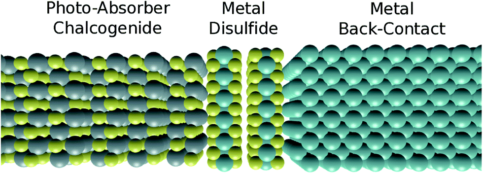 | ||
| Fig. 1 Illustrative schematic of materials configuration considered in this work. While two atomic layers of an interlayer disulfide material are shown explicitly in this case, no assumptions are made as to the number of layers in these scenarios. | ||
2 Computational procedure
The electronic properties were derived using Kohn–Sham DFT,13,14 within the plane-wave projector augmented-wave (PAW) formalism as implemented in the Vienna ab initio simulation package.15,16 Electron exchange and correlation interactions were described with the semi-local generalized gradient approximation (GGA) within the functional of Perdew, Burke and Ernzerhof (PBE).17 A plane-wave basis set (550 eV kinetic energy cut-off) was employed with well converged k-point sampling.18 Relaxations were undertaken for the metallic, CIS and CZTS materials, with a force convergence criterion of 0.005 eV Å−1 for the conjugate-gradient algorithm and an SCF convergence of 10−7 eV. However, in order to preserve the 2-dimensional structural characteristics of SnS, SnS2, MoS2, TiS2, WS2 and ZrS2 structural relaxations were not performed. Justification for this decision based on the explicit failure of standard local, semilocal, and hybrid functionals used in (hybrid) DFT calculations methods to recover experimental parameters upon relaxation for SnS2 can be found in the literature.19 The lattice constants for the 2-dimensional compounds are shown in Table 1.| Compound | a | b | c | α | β | γ |
|---|---|---|---|---|---|---|
| Mo2 | 3.160 | 3.160 | 12.320 | 90 | 90 | 120 |
| SnS | 11.180 | 3.982 | 4.329 | 90 | 90 | 90 |
| SnS2 | 3.649 | 3.649 | 5.899 | 90 | 90 | 120 |
| TiS2 | 3.412 | 3.412 | 5.695 | 90 | 90 | 120 |
| WS2 | 3.140 | 3.140 | 12.30 | 90 | 90 | 120 |
| ZrS2 | 3.650 | 3.650 | 5.810 | 90 | 90 | 120 |
In order to provide a quantitative electronic predictions of band gaps, work functions and ionisation potentials,20 hybrid-DFT was employed for semiconducting compounds by incorporating 25% Hartree–Fock exchange with the screening distance of 0.208 Å−1 to produce the HSE06 functional.21,22 The metals were treated with PBE and the Methfessel–Paxton scheme for partial occupancies,23 with a smearing width of 0.2 eV. A Gaussian smearing width of 0.05 eV was used for the semiconductors.
The crystal structures are the known geometries for each phase at room temperature. The corresponding symmetries for each are Mo: Im![[3 with combining macron]](https://www.rsc.org/images/entities/char_0033_0304.gif) m, Sn: I41/amd, Ti: P6/mmm, W: Imm and SnS: Pmcn, CuInS2: I
m, Sn: I41/amd, Ti: P6/mmm, W: Imm and SnS: Pmcn, CuInS2: I![[4 with combining macron]](https://www.rsc.org/images/entities/char_0034_0304.gif) 2d, Cu2ZnSnS4: I.
2d, Cu2ZnSnS4: I.
Values of work function and ionisation potential (ϕ) were found by shifting the highest occupied eigenvalue of the bulk structure by the energy difference between the vacuum level of the slab calculations and the macroscopic planar average of the ionic and Hartree potential for the slab (excluding the exchange correlation potential), (ΔV), according to eqn (1).24,25
| ϕ = ΔV − EF | (1) |
The cleavage planes correspond to the terminations described in the text and were not allowed to relax. None of the surfaces were found to be polar.
3 Results
3.1 Photoactive sulfides
The materials SnS, CIS and CZTS adopt the herzenbergite, chalcopyrite and kesterite structures respectively, as shown in Fig. 2. The herzenbergite structure is an arrangement of corner sharing polyhedra where, in the case of SnS, the Sn2+ lone pair repulsion gives rise to a pseudo-layered structure, similar to that of black phosphorous.29 The chalcopyrite structure can be considered as two inter-penetrating face centred cubic lattice arrangements of zincblende or diamond structure, one devoted to the anion locations (S2−) and one to the cation sites (Cu+ & In3+). The kesterite structure is a derivative of the chalcopyrite phase, maintaining the nearly cubic close-packed lattice of S anions but with the B-site cations occupied by two different cations rather than one.30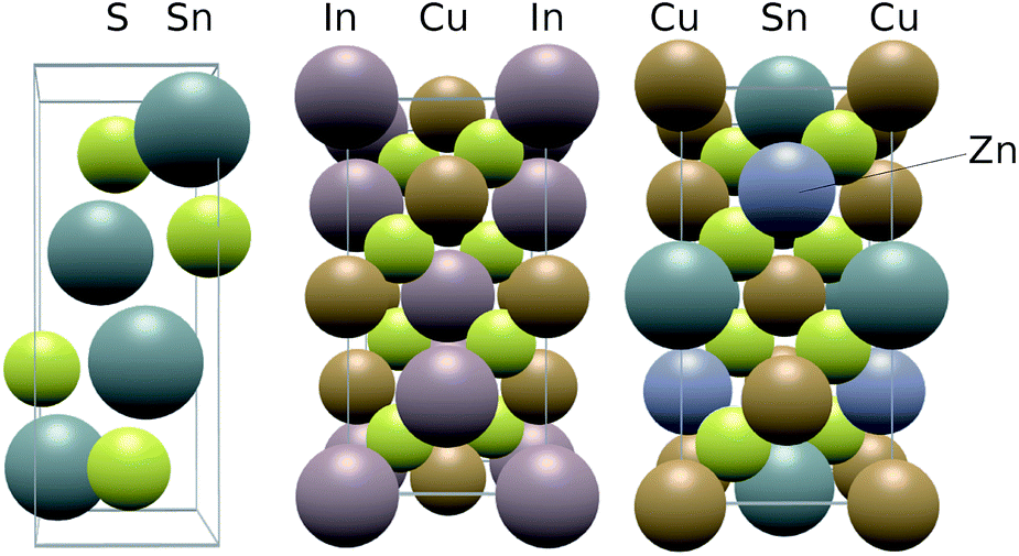 | ||
| Fig. 2 Structure of the photoactive sulfides studied in this work, from left to right: herzenbergite SnS, chalcopyrite CIS and kesterite CZTS. | ||
The materials SnS, CIS and CZTS exhibit promising electro-optical properties. For example, SnS has a higher optical absorption coefficient than CdTe, (>105 cm−1 above 1.3 eV)31 and internal quantum efficiencies higher than 90% in the visible light range,32 yet the certified efficiencies obtained by experiment are less than a quarter of those of CdTe.4 Likewise, CIS and CZTS both underperform compared to CISe and CZTSe respectively. This is especially interesting considering that the band gap of CZTS is more optimal with respect to the Schockley–Quiesser limit than the selenide analogue,33 (1.48–1.63 eV,28 compared to 0.97 eV,34 respectively). For CZTS the higher efficiency reported with the selenide material is 9.7%,34versus 8.4% for the sulfide (the current record of 12.6% was achieved with a mixed sulfur/selenium quinternary material).35 Similarly, CuInS2 has a reported band gap of around 1.5 eV,27 which is more optimal than that of CuInSe2 (around 1.0 eV),36 and yet the record for CuInS2 stands at 12.5%,37 while the CuInSe2 record efficiency is much higher (20.9%).38 Such a deviation from expected behaviour is indicative of poor band alignment of the sulfide absorber material with respect to the other components in the device. These facts are summarised in Fig. 3 alongside the record efficiencies of alternate successful PV materials.
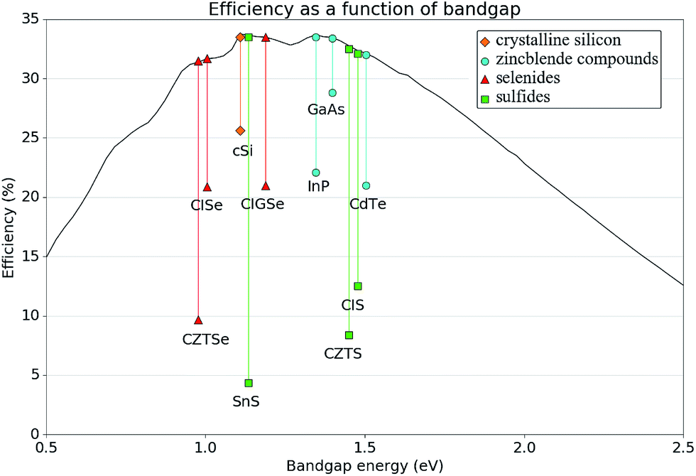 | ||
| Fig. 3 Schematic illustrating the Schockley–Quiesser photovoltaic efficiency limit as a function of band gap, and the record certified efficiencies to date of specifical successful photovoltaic materials. The key indicates groups of similar compounds, showing for example, how sulfides have consistently underperformed to date, when compared with other materials. | ||
Of course, the band gap of a material is not the sole property dictating device performance. However, it has been reported that the lower efficiencies of these sulfide, namely CuInS2, cells underperform due to low open-circuit voltage, while having a short circuit current comparable to the world record efficiency solar cells.39 This is again indicative of poor band alignment as a wider band gap material should not suffer from a lower open circuit voltage than a lower band gap material.
The band gaps of the three photo-active sulfides and the corresponding ionisation potentials from our level of theory are shown in Table 2. The band gap of the CIS is slightly lower than the value of the optimum band gap of photovoltaic efficiency according the Shockley–Quisser limit, but is direct according to our calculations. The gap of CZTS is more optimal than CIS and is also direct. SnS has the least optimal fundamental band gap and it is indirect in nature, but is almost identical to silicon, the most widely used photovoltaic material. Overall, the theoretically calculated values show good agreement with experiment, given the chemically complex nature of the systems considered (Sn stereoactive lone pairs, Cu 3d states and competing phases in characterised films).
The ionisation potentials are calculated from the SnS(100), CIS(110) and CZTS(100) crystal terminations. For CZTS the slab configuration was generated using the procedure reported previously by Hinuma et al.,40 whereby selected atoms are removed to maintain stoichiometry and non-polarity. The geometry of such a configuration is shown in Fig. 4 along with the electrostatic potential resulting from the calculation.
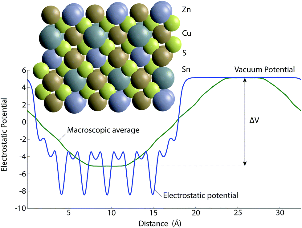 | ||
| Fig. 4 The slab model for calculating the ionisation potential of CZTS showing both the symmetrical slab and the electrostatic potential of a non-polar termination from which the difference between bulk and vacuum potential (ΔV) can be found to calculate ionisation potential or work function (eqn (1)). The yellow, bronze, blue and grey spheres correspond to sulfur, copper, tin and zinc atoms respectively. | ||
At this point we uncover the first potential problem with the sulfide photoabsorbers. SnS is a commonly observed imperfection in CZTS synthesis,41 and one can deduce from the ionisation potential and band gap values of Table 2 that any SnS present in a CZTS would form a type 3, broken gap, heterojunction. That is to say that any SnS material contacting bulk CZTS, either within the material or at an interface, would provide a location for charge recombination and adversely affect performance of a CZTS photovoltaic device. While this is certainly an important consideration for CZTS optimisation it does not provide an explanation as to how all of the three materials under-perform and further considerations must be made in our investigation.
3.2 Metals
The desirability of sulfides as earth abundant materials has long been established,43 therefore it would be self-defeating to seek device contacts that are themselves rare or expensive. For this reason the commonly used gold, silver or platinum contacts are excluded. Similarly, toxic metals are excluded as the necessary precautions and procedures surrounding the treatment of such materials can elevate costs significantly.Several papers report the use of copper as an electrode for chalcogenide contact,44,45 which, while desirable due to abundance and cost factors, is known to diffuse into contacting solids, to the detriment of device behaviour.46,47 The current method of dealing with this problem requires additional deposition of diffusion barrier materials, increasing cost and chemical complexity, and so Cu is also discounted.
The metals selected for consideration in this work are chosen not only due to cost abundance factors but also mechanical suitability and simplicity; these are molybdenum, tin, titanium, tungsten and zirconium. It is important to note that although tin is known to undergo a transition to a zero band gap semiconductor (α Sn) at low temperatures, sufficient high purity tin can resist degradation to below −30 °C,48,49 and so the metallic phase (β Sn) is still suitable for inclusion in this study. Molybdenum is already a commonly employed back contact in sulfide photovoltaics,50 largely due to its success in selenide and telluride PV deployment, which allows for direct comparison between our results and experimental observations in the literature.‡
Metals are characterised by high conductivity and mobile electrons. The work function of a metal is its Fermi level with respect to the vacuum, which determines the barrier height at a metal–semiconductor junction. The sulfides considered in this work are known to exhibit p-type conductivity,51–53 where the majority and minority carriers are collected at the back and front contact, respectively. Therefore, in order for a photovoltaic device to operate as effectively as possible the Fermi level of the contact metal ought to be slightly lower in magnitude than the valence band maximum of a p-type absorber component. This slight off-set provides the localised field effect that is the driving force for the hole migration towards the interface and ultimate extraction (often referred to as the depletion region).54
Earlier work has shown the importance of the band alignment between photo-absorber and device contacts,9 where it was explicitly concluded that molybdenum is an unsuitable contact, for SnS at least, despite the fact that the record efficiencies for the material were reported using this device architecture (below 5%).55
The calculated work functions for the selected metals at the indicated crystallographic terminations are reported in Table 3, along with collected values from the literature. The agreement between experiment and theory appears good overall and our calculations agree with previous calculations for similar level of theory.56 It ought to be remembered that there are great difficulties in measuring a work function accurately using surface sensitive techniques coupled with the potential surface oxidation/contamination of the metals. For example, the work function of gold can vary by up to 1 eV depending on surface treatment.57
| Metal | System | Theoretical work function (surface plane) | Experimental work function (surface plane) | ||||
|---|---|---|---|---|---|---|---|
| Mo | Cubic | 3.93 (100) | 4.70 (110) | 3.71 (111) | 4.53 (100) | 4.95 (110) | 4.55 (111) |
| Sn | Tetragonal | 3.96 (100) | 4.02 (010) | 3.01 (001) | |||
| Ti | Hexagonal | 4.35 (0001) | 4.3 (poly) | ||||
| W | Cubic | 4.17 (100) | 4.87 (110) | 3.94 (111) | 4.63 (100) | 5.25 (110) | 4.47 (111) |
| Zr | Hexagonal | 4.11 (0001) | 4.1 (poly) | ||||
The strong dependence of metal work function on crystal termination for the cubic systems, i.e. molybdenum and tungsten, relates directly to the packing density of the crystal surfaces in question, following the so called Smoluchowski model.58 Such information in this case could be useful in selecting device components for robust performance at lower cost, by using contacts that have relatively consistent work functions with respect to surface orientation, necessitating less care with contact deposition, as multiple grain orientations induce less work function variability.
At this stage it is possible to identify the most ideal contacts from band offsets as those metal surfaces with work functions as close to the ionisation potential of the associated sulfides, while still being higher in energy to drive the hole extraction across the material interface. For SnS the 4.35 eV work function of Ti is optimal, for CIS and CZTS the W(110) surface is most optimal although this is close in energy to the Mo(110) surface; Mo being the contact of choice already for these systems.
Unfortunately, it has been repeatedly observed that such perfectly segregated materials interfaces are rare – almost always some degree of interface reaction occurs between two contacting materials. Accounting for such occurrences is possible with modern DFT methods but rarely seen in the literature. Here we continue on to explore the possibility of 2-dimensional metal-disulfide formation between the bulk materials using the principles of thermodynamics.
3.3 Formation of disulfides
In unreactive systems the results presented in the previous section could be used to inform the selection of device components – the closest value of the metal work functions to that of the chalcogenide, while still being lower in magnitude, would represent the optimal contact. However, it is known that reactions or reconstructions naturally occur at solid contacts as dangling bonds from surface cleavage reform across the materials interface. Evidence of metal disulfide formation at chalcogenide – metal interfaces has been presented in the literature, for SnS and CZTS explicitly,59,60 even on the nanometer scale,59 which has been shown to be sufficient in affecting the formation of an ohmic contact.61Simple thermodynamic arguments have already been shown to play a fundamental role in the design, optimisation and performance of solar cell devices, due to issues associated with phase mixing and separation across interfaces.41 As such, the possibility of the formation of relevant disulfides is explored in this section by calculating the enthalpies of degradation reactions shown in Table 4. It should be noted that the following chemical reactions were also considered but had no negative enthalpies (i.e. thermodynamically not favourable), except in the case of reaction number 3 for M = Zr, which has a favourable formation energy of −0.71 eV.
| M(s) + 2CuInS2(s) → MS2(s) + Cu2S(s) + 2InS(s) | (2) |
| M(s) + 2Cu2ZnSnS4(s) → MS2(s) + 4Cu(s) + 2ZnS(s) + 2SnS2(s) | (3) |
| M(s) + 2Cu2ZnSnS4(s) → MS2(s) + 2Cu2S(s) + 2Zn(s) + 2SnS2(s) | (4) |
| Degradation reaction | Reaction energy w (eV) |
|---|---|
| Mo + 2SnS → MoS 2 + 2Sn | −0.63 |
| Sn + 2SnS → SnS2 + 2Sn | 0.57 |
| Ti + 2SnS → TiS2 + 2Sn | 1.87 |
| W + 2SnS → WS 2 + 2Sn | −0.45 |
| Zr + 2SnS → ZrS 2 + 2Sn | −2.73 |
| Mo + CuInS 2 → MoS 2 + Cu + In | −0.61 |
| Sn + CuInS2 → SnS2 + Cu + In | 0.58 |
| Ti + CuInS2 → TiS2 + Cu + In | 1.89 |
| W + CuInS 2 → WS 2 + Cu + In | −0.44 |
| Zr + CuInS 2 → ZrS 2 + Cu + In | −2.72 |
| Mo + 2Cu 2 ZnSnS 4 → MoS 2 + 2Cu 2 S + 2ZnS + 2SnS | −1.04 |
| Sn + 2Cu2ZnSnS4 → SnS2 + 2Cu2S + 2ZnS + 2SnS | 0.16 |
| Ti + 2Cu2ZnSnS4 → TiS2 + 2Cu2S + 2ZnS + 2SnS | 1.46 |
| W + 2Cu 2 ZnSnS 4 → WS 2 + 2Cu 2 S + 2ZnS + 2SnS | −0.86 |
| Zr + 2Cu 2 ZnSnS 4 → ZrS 2 + 2Cu 2 S + 2ZnS + 2SnS | −3.14 |
Besides these reactions, there are alternate phases that might be accessible for the systems considered, such as metallic TiS for the titanium contact case, or SnS for Sn.62 However, as these are are 3-dimensional materials, their formation is not as likely to block large areas of charge transfer at the device interface or be as difficult to detect as the interlayer formation of the 2-dimensional materials.
These results show that each chalcogenide has a favourable enthalpy for chemical degradation with molybdenum, tungsten and zirconium. Perhaps this is the origin of the relatively poor performance of the sulfide materials in devices. By contrast none of these sulfides are expected to degrade with contacting solid tin or titanium. The positive enthalpies associated with the tin case are also produced when considered with respect to α tin, rather than β tin, showing that this effect is not an artefact of using the metastable material structure. To the authors knowledge neither tin nor titanium have been used as a device contact to date.
Also of importance, are the multiple secondary components expected to be produced from the thermodynamically favourable CZTS degradation, in agreement with observations in the literature.63 Zinc chalcogenide formation has been observed at CZTSe–Mo interfaces in agreement with the results reported here.64 Such a complex mixture of compounds is expected to cause a wide variety in performances obtained for this material.
An important conclusion therefore is that most, if not all, sulfide devices fabricated to date could have a disulfide intermediate layer, or even form them over the course of the repeated heating and cooling associated with photovoltaic operation. Countless papers report the observation of interstitial stoichiometric variance when viewed on a small enough scale59,65 but there is confusion in the literature regarding their likely effects.60,66 These processes are not necessarily of detriment to device performance, indeed, composition inter-diffusion between contacts is deliberately induced between components for CdTe PV cells in order to achieve the highest device efficiencies.67 There have been conflicting reports on the likely effect of MoS2 formation on the performance of CZTS cells in the literature, while it is thought that MoSe2 has a beneficial effect in CIGSe cell device performance.61 We attempt to clarify the likely effects of these predicted structures in the subsequent section.
3.4 Energy levels of disulfides
Having established the likelihood of disulfide formation from a thermodynamic stand point, it is natural to consider the electronic effects of their formation. It has been repeatedly demonstrated that transition metal disulfides form high resistance contacts with metals,77 which would lead to the assumption that any presence of an MS2 species would be problematic. On the contrary, MoSe2 at least, has shown to have a beneficial effect in CIGSe cell device performance.61 As such we again employ the principles of band alignment to further elucidate the effects of such interlayer phases might have on performance.Firstly, it should be stated that our calculations indicate that the valence band maximum of disulfide layers protrudes above and below the bonded plane, as shown in Fig. 5. Given that this is the band preferentially occupied by positive charge carriers (holes), and are considered to be in contact with p-type photoabsorbers, an ohmic contact can be maintained between the bulk materials if the interstitial phase is parallel to the junction, and so the validity of our model is maintained. A study on the interface of SnS and SnS2 also concluded charge transfer between the two materials is possible.78
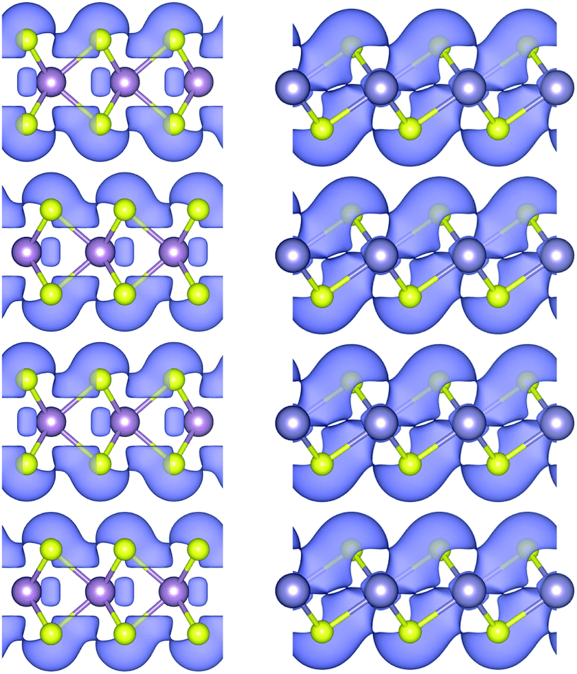 | ||
| Fig. 5 Highest occupied molecular orbitals for MoS2 (left) and SnS2 (right), which are isostructural with WS2 and TiS2/ZrS2 respectively. | ||
The fundamental band gap values and work functions for the disulfides are shown in Table 5, showing good agreement in their comparison with experiment. In these calculations, the surface is taken as the natural (001) termination as each disulfide forms a 2-dimensional structure with relatively weak van der Waals layers in the c direction. Technically, such terminations for these systems are Tasker type II interfaces surfaces and, while not polar or unstable, do contain an inbuilt local dipole arising from the Y−X+Y− atomic arrangements of the XY2 compounds.79 The reasons for deciding to use these surfaces are two-fold. Firstly, adhering to the triple-junction model displayed in Fig. 1 and maintained throughout this study, a charge transition from the metal to the calchogenide would experience this same dipole i.e. it is a real effect and not an artefact of our calculation. Secondly, as already mentioned the 2-dimensional disulfides were not allowed to relax to preserve their VDW structure recovered from experiment and not yet properly accounted for in standard local, semilocal, and hybrid functionals. To form a Tasker type I interface the atomic bonds of the crystal would need to be cleaved resulting in artificially high energy without relaxation. In order to keep the calculations consistent throughout, the decision was made to use the Tasker type II interfaces. However, it has been found that the type I, (110) surface reproduces excellent agreement with single crystal experiments,19,80 and we encourage any authors of future work to consider their choice of crystal termination carefully.
4 Discussion
All of the results from this work are summarised schematically in a hypothetical horizontal contact arrangement, with the disulfide situated between the chalcogenides and metal surfaces, in Fig. 6. This is deliberately arranged to represent the band levels of the hypothetical triple-junction contact shown in Fig. 1, where a positive charge carrier would migrate from left to right.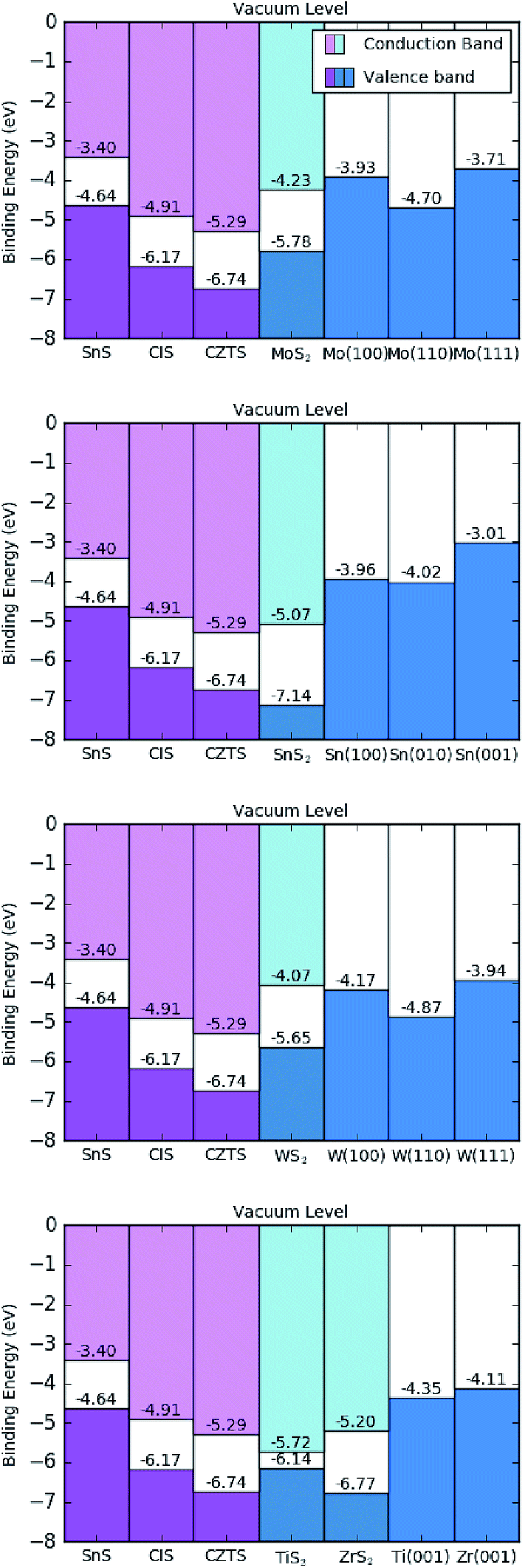 | ||
| Fig. 6 Calculated band offset diagram, using the HSE06 functional, for hypothetical sulfide contacts with indicated metal surfaces. The materials are ordered, from left to right, as the sulfide photo-absorber material, disulfide interlayer and metallic contact; as illustrated in Fig. 1. Ti and Zr scenarios are displayed in the same diagram (bottom). | ||
The values of the work function for all of the disulfides are greater in magnitude than the work functions of the metals considered, as shown in Table 3. This result agrees with chemical intuition as the MS2 species have a high elemental ratio of the relatively electronegative sulfur, leading to more strongly bound electrons; but there is a more diverse relationship between the disulfides and the photoactive sulfides being considered. All of the disulfides have deeper energy levels than SnS, meaning any disulfide interlayer formation will result in a hole blocking layer and reduce the performance of SnS. This could be why SnS has the lowest performance, to date, of the three sulfides considered. CIS would appear to make favourable contact with MoS2 and TiS2, where the VBMs are slightly higher in energy than those of CIS. Of the two, however, MoS2 appears a superior contact, as the subsequent metal junction Fermi level of Mo is closer in energy to the VBM of CIS and represents a lower level of energy loss from hole thermalisation than does Ti metal. CZTS would make favourable contact with all of the disulfides except SnS2 and ZrS2, although the energy levels are so similar between ZrS2 and CZTS that one wouldn't expect it to cause a significant performance loss. Taking into account both disulfide and metal contacts, tungsten would appear to be an optimal contact for CZTS, as the energy levels of W metal are slightly deeper than those of Mo, representing a smaller loss of open circuit voltage.
If one now considers all information presented in this work, i.e. the thermodynamic driving force for contact degradation from the previous section and the energetic effects of the products of such a reaction it is possible to conclude with an overall optimal contact for each photoactive sulfide material. For SnS, titanium metal has a Fermi-level closest to the VBM, and would not react to form a 2 dimensional interlayer but care should still be taken to avoid the formation of 3-dimensional TiS where possible. For CIS and CZTS tungsten appears to be an optimal contact, even though the interstitial disulfide is expected to form our energy-level calculations predict that it would act as a buffer layer between the photoactive material and the W contact. At least, this study is able to conclude that better performance ought to be possible with W compared to Mo, as the chemistry is virtually identical while the W metal contact has lower energy levels than Mo for the same crystallographic terminations. Based on the principles of band alignment, such a substitution of W for the commonly used Mo should recover some of the lost open circuit voltage observed in the literature. Of course, this is discounting the energetic effects of the numerous other sulfide components produced from the CZTS decomposition shown in Table 4, but is supported by the observation that tungsten was shown to be a superior contact over Mo, Cr, Ta, Nb, V, Ti, Mn in the experiment for CIGSe, a similarly quaternary material able to form interstitial WSe2.12
5 Conclusions
We have shown the theoretical basis for the long acknowledged axiom of interstitial compound formation in photovoltaics based on the principles of band alignment and calculated reaction energies.Given that low open circuit voltage has been shown to be one of the major issues plaguing these systems, we are able to show, based on the principles of band alignment, that the most ideal contacts are titanium for SnS and tungsten for CIS and CZTS as they should result in the lowest voltage loss for holes migrating across the back contact interface. Similarly, we show that molybdenum, one of the most commonly used contacts is a poor fit for all cases. It is expected that these results can facilitate the further integration of more earth-abundant materials into photovoltaic devices, driving down costs and issues associated with materials availability.
We are also able to highlight the detrimental effects on photovoltaic performance that are likely to result from layered disulfide formation and from SnS impurities present in a CZTS sample. We conclude that the formation of such impurity sulfides should be suppressed as much as possible to maximise performance but also show the extent to which such impurities can be unavoidable if greater care is not taken when selecting components for device configurations.
Finally, while considered impurities in this work, the layered disulfides could provide more sustainable alternatives to the widely used CdS buffer layer based on band alignments for electron extraction. We hope that the data in this paper can encourage more diversity in device design used in future work.
Acknowledgements
LAB is an International Research Fellow of the Japan Society of Promotion of Science (JSPS) (grant number 26.04792). This work was also supported by a Grant-in-Aid for Young Scientists (A) (grant No. 15H05541) and Scientific Research (B) (grant No. 15H04125) from JSPS and MEXT Elements Strategy Initiative to Form Core Research Center. The computing resources of ACCMS at Kyoto University were used in this work.References
- J. Jean, P. R. Brown, R. L. Jaffe, T. Buonassisi and V. Bulovic, Energy Environ. Sci., 2015, 8, 1200–1219 CAS.
- K. R. Reddy, N. K. Reddy and R. Miles, Sol. Energy Mater. Sol. Cells, 2006, 90, 3041–3046 CrossRef.
- A. Klein, J. Phys.: Condens. Matter, 2015, 27, 134201 CrossRef PubMed.
- M. A. Green, K. Emery, Y. Hishikawa, W. Warta and E. D. Dunlop, Prog. Photovoltaics, 2016, 24, 905–913 Search PubMed.
- R. Scheer and H. Schock, Chalcogenide Photovoltaics: Physics, Technologies, and Thin Film Devices, Wiley, 2011 Search PubMed.
- I. Lange, S. Reiter, M. Patzel, A. Zykov, A. Nefedov, J. Hildebrandt, S. Hecht, S. Kowarik, C. Woll, G. Heimel and D. Neher, Adv. Funct. Mater., 2014, 24, 7014–7024 CrossRef CAS.
- P. Sinsermsuksakul, K. Hartman, S. B. Kim, J. Heo, L. Sun, H. H. Park, R. Chakraborty, T. Buonassisi and R. G. Gordon, Appl. Phys. Lett., 2013, 102, 053901 CrossRef.
- F.-L. Kuo, Y. Li, M. Solomon, J. Du and N. D. Shepherd, J. Phys. D: Appl. Phys., 2012, 45, 065301 CrossRef.
- L. A. Burton and A. Walsh, Appl. Phys. Lett., 2013, 102, 132111 CrossRef.
- M. Devika, N. K. Reddy, D. S. Reddy, Q. Ahsanulhaq, K. Ramesh, E. S. R. Gopal, K. R. Gunasekhar and Y. B. Hahn, J. Electrochem. Soc., 2008, 155, H130–H135 CrossRef CAS.
- D.-C. Nguyen, K. Takehara, T. Ryo and S. Ito, Energy Procedia, 2011, 10, 49–54 CrossRef CAS.
- K. Orgassa, H. Schock and J. Werner, Thin Solid Films, 2003, 431–432, 387–391 CrossRef CAS.
- P. Hohenberg and W. Kohn, Phys. Rev., 1964, 136, B864–B871 CrossRef.
- W. Kohn and L. J. Sham, Phys. Rev., 1965, 140, A1133–A1138 CrossRef.
- G. Kresse and J. Furthmüller, Phys. Rev. B: Condens. Matter Mater. Phys., 1996, 54, 11169 CrossRef CAS.
- G. Kresse and D. Joubert, Phys. Rev. B: Condens. Matter Mater. Phys., 1999, 59, 1758 CrossRef CAS.
- J. P. Perdew, K. Burke and M. Ernzerhof, Phys. Rev. Lett., 1996, 77, 3865–3868 CrossRef CAS PubMed.
- J. Moreno and J. M. Soler, Phys. Rev. B: Condens. Matter Mater. Phys., 1992, 45, 13891–13898 CrossRef.
- L. A. Burton, T. J. Whittles, D. Hesp, W. M. Linhart, J. M. Skelton, B. Hou, R. F. Webster, G. O'Dowd, C. Reece, D. Cherns, D. J. Fermin, T. D. Veal, V. R. Dhanak and A. Walsh, J. Mater. Chem. A, 2016, 4, 1312–1318 CAS.
- T. L. Bahers, M. Rerat and P. Sautet, J. Phys. Chem. C, 2014, 118, 5997–6008 CAS.
- J. Heyd, G. E. Scuseria and M. Ernzerhof, J. Chem. Phys., 2006, 124, 219906 CrossRef.
- A. V. Krukau, O. A. Vydrov, A. F. Izmaylov and G. E. Scuseria, J. Chem. Phys., 2006, 125(22), 224106 CrossRef PubMed.
- M. Methfessel and A. T. Paxton, Phys. Rev. B: Condens. Matter Mater. Phys., 1989, 40, 3616–3621 CrossRef CAS.
- J. Jackson, Classical Electrodynamics, Wiley, 1975 Search PubMed.
- K. T. Butler, J. Buckeridge, C. R. A. Catlow and A. Walsh, Phys. Rev. B: Condens. Matter Mater. Phys., 2014, 89, 115320 CrossRef.
- T. J. Whittles, L. A. Burton, J. M. Skelton, A. Walsh, T. D. Veal and V. R. Dhanak, Chem. Mater., 2016, 28, 3718–3726 CrossRef.
- D. Mitzi, Solution Processing of Inorganic Materials, Wiley, 2008 Search PubMed.
- C. Malerba, F. Biccari, C. L. A. Ricardo, M. Valentini, R. Chierchia, M. Muller, A. Santoni, E. Esposito, P. Mangiapane, P. Scardi and A. Mittiga, J. Alloys Compd., 2014, 582, 528–534 CrossRef CAS.
- X. Ling, H. Wang, S. Huang, F. Xia and M. S. Dresselhaus, Proc. Natl. Acad. Sci. U. S. A., 2015, 112, 4523–4530 CrossRef CAS PubMed.
- J. Scragg, Copper Zinc Tin Sulfide Thin Films for Photovoltaics: Synthesis and Characterisation by Electrochemical Methods, Springer, Berlin Heidelberg, 2011 Search PubMed.
- Y.-B. Yang, J. K. Dash, Y. Xiang, Y. Wang, J. Shi, P. H. Dinolfo, T.-M. Lu and G.-C. Wang, J. Phys. Chem. C, 2016, 120, 13199–13214 CAS.
- P. Sinsermsuksakul, L. Sun, S. W. Lee, H. H. Park, S. B. Kim, C. Yang and R. G. Gordon, Adv. Energy Mater., 2014, 1400496 CrossRef.
- W. Shockley and H. J. Queisser, J. Appl. Phys., 1961, 32, 510–520 CrossRef CAS.
- G. Brammertz, M. Buffiere, S. Oueslati, H. ElAnzeery, K. Ben Messaoud, S. Sahayaraj, C. Koble, M. Meuris and J. Poortmans, Appl. Phys. Lett., 2013, 103(16), 163904 CrossRef.
- B. Shin, O. Gunawan, Y. Zhu, N. A. Bojarczuk, S. J. Chey and S. Guha, Prog. Photovoltaics, 2013, 21, 72–76 CAS.
- S. Chichibu, T. Mizutani, K. Murakami, T. Shioda, T. Kurafuji, H. Nakanishi, S. Niki, P. J. Fons and A. Yamada, J. Appl. Phys., 1998, 83, 3678–3689 CrossRef CAS.
- M. Lux-Steiner, A. Ennaoui, C.-H. Fischer, A. Jager-Waldau, J. Klaer, R. Klenk, R. Konenkamp, T. Matthes, R. Scheer, S. Siebentritt and A. Weidinger, Thin Solid Films, 2000, 361–362, 533–539 CrossRef CAS.
- S. Frontier, Solar Frontier Sets Thin-Film PV World Record with 20.9Cell, Fraunhofer institute technical report, 2014 Search PubMed.
- M. H. Jin, K. K. Banger, C. V. Kelly, J. H. Scofield, J. S. Mcnatt and J. E. Dickman, Proceedings of the 19th European Photovoltaic Solar Energy Conference, 2004 Search PubMed.
- Y. Hinuma, Y. Kumagai, F. Oba and I. Tanaka, Comput. Mater. Sci., 2016, 113, 221–230 CrossRef CAS.
- J. J. Scragg, P. J. Dale, D. Colombara and L. M. Peter, ChemPhysChem, 2012, 13, 3035–3046 CrossRef CAS PubMed.
- A. Goldmann, H. Landolt and R. Börnstein, Electronic Structure of Solids: Subvol. C1, Springer, 1989 Search PubMed.
- C. Wadia, A. P. Alivisatos and D. M. Kammen, Energy Environ. Sci., 2009, 43, 2072–2077 CAS.
- T. Ikuno, R. Suzuki, K. Kitazumi, N. Takahashi, N. Kato and K. Higuchi, Appl. Phys. Lett., 2013, 102, 193901 CrossRef.
- S. G. Kumar and K. S. R. K. Rao, Energy Environ. Sci., 2014, 7, 45–102 CAS.
- R. Saraf, IOSR-Journal of Electrical and Electronics Engineering, 2012, 2, 47 CrossRef.
- P. Majumder, U. of Illinois at Chicago, Fundamental Studies of Diffusion Barriers for Copper Metallization and Atomic Layer Deposited High-kappa Films, University of Illinois at Chicago, 2008 Search PubMed.
- F. Vnuk, A. DeMonte and R. Smith, Mater. Lett., 1983, 2, 67–70 CrossRef CAS.
- J. Levy, Tin, Rosen Publishing Group, 2009 Search PubMed.
- K. Roebuck, Photovoltaics (PV): High-impact Strategies – What You Need to Know: Definitions, Adoptions, Impact, Benefits, Maturity, Vendors, Emereo Publishing, 2012 Search PubMed.
- L. A. Burton, D. Colombara, R. D. Abellon, F. C. Grozema, L. M. Peter, T. J. Savenije, G. Dennler and A. Walsh, Chem. Mater., 2013, 25, 4908–4916 CrossRef CAS.
- J. Gonzalez, J. A. Torres and G. S. Perez, Phys. Status Solidi B, 1982, 69, K37–K41 CrossRef CAS.
- D. Dumcenco and Y.-S. Huang, Opt. Mater., 2013, 35, 419–425 CrossRef CAS.
- J. Nelson, The Physics of Solar Cells, Imperial College Press, 2003 Search PubMed.
- P. Sinsermsuksakul, R. Chakraborty, S. B. Kim, S. M. Heald, T. Buonassisi and R. G. Gordon, Chem. Mater., 2012, 24, 4556 CrossRef CAS.
- H. L. Skriver and N. M. Rosengaard, Phys. Rev. B: Condens. Matter Mater. Phys., 1992, 46, 7157–7168 CrossRef CAS.
- A. Kahn, Mater. Horiz., 2016, 3, 7–10 RSC.
- R. Smoluchowski, Phys. Rev., 1941, 60, 661–674 CrossRef CAS.
- A. Schneikart, H.-J. Schimper, A. Klein and W. Jaegermann, J. Phys. D: Appl. Phys., 2013, 46, 305109 CrossRef.
- J. J. Scragg, J. T. Watjen, M. Edoff, T. Ericson, T. Kubart and C. Platzer-Bjorkman, J. Am. Chem. Soc., 2012, 134, 19330–19333 CrossRef CAS PubMed.
- S. Nishiwaki, N. Kohara, T. Negami and T. Wada, Jpn. J. Appl. Phys., 1998, 37, L71–L73 CrossRef CAS.
- L. A. Burton and A. Walsh, J. Phys. Chem. C, 2012, 116, 24262–24267 CAS.
- J. J. Scragg, T. Kubart, J. T. Watjen, T. Ericson, M. K. Linnarsson and C. Platzer-Bjorkman, Chem. Mater., 2013, 25, 3162–3171 CrossRef CAS.
- S. Ahn, S. Jung, J. Gwak, A. Cho, K. Shin, K. Yoon, D. Park, H. Cheong and J. H. Yun, Appl. Phys. Lett., 2010, 97, 021905 CrossRef.
- D. Abou-Ras, G. Kostorz, D. Bremaud, M. Kalin, F. Kurdesau, A. Tiwari and M. Dobeli, Thin Solid Films, 2005, 480–481, 433–438 CrossRef CAS.
- P. Chelvanathan, M. I. Hossain, J. Husna, M. Alghoul, K. Sopian and N. Amin, Jpn. J. Appl. Phys., 2012, 51, 10NC32 CrossRef.
- B. E. McCandless, M. G. Engelmann and R. W. Birkmire, J. Appl. Phys., 2001, 89, 988–994 CrossRef CAS.
- G. Hodes, Chemical Solution Deposition Of Semiconductor Films, Taylor & Francis, 2002 Search PubMed.
- R. H. Williams and A. J. McEvoy, Phys. Status Solidi B, 1971, 47, 217–224 CrossRef CAS.
- J. George and K. S. Joseph, J. Phys. D: Appl. Phys., 1982, 15, 1109 CrossRef CAS.
- Electron Spectroscopies Applied to Low-dimensional Structures, ed. H. P. Hughes and H. I. Starnberg, Kluwer Academic Publishers, Dordrecht, 2001 Search PubMed.
- F. R. Shepherd and P. M. Williams, J. Phys. C: Solid State Phys., 1974, 7, 4416–4426 CrossRef CAS.
- E. E. Krasovskii and V. N. Strocov, J. Phys.: Condens. Matter, 2009, 21, 314009 CrossRef CAS PubMed.
- D. Braga, I. Gutierrez Lezama, H. Berger and A. F. Morpurgo, Nano Lett., 2012, 12, 5218–5223 CrossRef CAS PubMed.
- S. Fiechter, Sol. Energy Mater., 2004, 83, 459–477 CrossRef CAS.
- D. Greenaway and R. Nitsche, J. Phys. Chem. Solids, 1965, 26, 1445–1458 CrossRef CAS.
- R. Kappera, D. Voiry, S. E. Yalcin, B. Branch, G. Gupta, A. D. Mohite and M. Chhowalla, Nat. Mater., 2014, 13, 1128–1134 CrossRef CAS PubMed.
- T. Lorenz, J.-O. Joswig and G. Seifert, Semicond. Sci. Technol., 2014, 29, 064006 CrossRef.
- P. W. Tasker, J. Phys. C: Solid State Phys., 1979, 12, 4977 CrossRef CAS.
- Y. Kumagai, L. A. Burton, A. Walsh and F. Oba, Phys. Rev. Appl., 2016, 6, 014009 CrossRef.
Footnotes |
| † Current address: Institute of Condensed Matter and Nanosciences, Université Catholique de Louvain, Chemin des Étoiles 8 bte L7.03.01 à 1348 Louvain-la-Neuve, Belgium, E-mail: E-mail: lee.burton@uclouvain.be. |
| ‡ Tungsten is cheaper than molybdenum per unit mass according to the US Geological Survey: http://minerals.usgs.gov/minerals/pubs/mcs/2015/mcs2015.pdf. |
| This journal is © The Royal Society of Chemistry 2017 |