
 Open Access Article
 This Open Access Article is licensed under a
 Creative Commons Attribution 3.0 Unported Licence
Metal-nanostructures – a modern and powerful platform to create transparent electrodes for thin-film photovoltaics
Kirill
Zilberberg
and
Thomas
Riedl
*
Institute of Electronic Devices, University of Wuppertal, Wuppertal, Germany. E-mail: t.riedl@uni-wuppertal.de; Fax: +49 202 439 1412; Tel: +49 202 439 1411
First published on 12th August 2016
Abstract
Thin-film solar technology is the subject of considerable current research. The classical material platform of amorphous silicon (a-Si) has been complemented by organic solar cells and more recently by solar cells based on quantum dots or organo-metal-halide perovskites. The majority of effort is focused on the synthesis, characterization and optimization of the photo-active components as well as on the invention of novel device architectures. Low-cost, low-weight, flexibility and the opportunity to create semi-transparent devices are among the most frequently claimed selling points of thin-film solar cells. It is clear that the full potential of this technology and the ability to fulfill its promises are intimately linked with tailored concepts for transparent electrodes beyond established avenues. Transparent electrodes, that can be realized at a large area, at low costs, at low temperature, which are flexible (or even elastic), and which afford a conductivity and transmittance even better than those of indium-tin-oxide, are still vigorously pursued. Even though metal based semi-transparent electrodes have a notable history, there is an ever increasing effort to unlock the full potential of metal nano-structures, especially ultra-thin films (2D) or metal-nanowires (1D) as semitransparent electrodes for thin-film solar cells. This article will review the most recent advances in semitransparent electrodes based on metal-nanowires or metal thin-films. Aside from providing general considerations and a review of the state of the art of electrode properties like sheet resistance and optical transmittance, we aim to highlight the current efforts to introduce these electrodes into solar cells. We will demonstrate that by the use of metal based semitransparent electrodes not only a replacement for established transparent conductors can be achieved but also novel functionalities can be envisaged.
 Kirill Zilberberg | Kirill Zilberberg studied at the South Ural State University in Russia and at the University of Wuppertal in Germany, where he received his Bachelor Sc. degree in IT in 2008 and Master Sc. degree in Electrical Engineering in 2010. In 2014, he received his PhD in the field of solution-processed interface materials for organic solar cells in the group of Prof. Riedl at the University of Wuppertal. As a post-doc he has been working on conjugated polyelectrolytes and electrode concepts for semi-transparent solar cells. |
 Thomas Riedl | Thomas Riedl received his PhD in physics from the TU Braunschweig in 2002. Heading the Advanced Semiconductors Group at the Institute of High-Frequency Technology, TU Braunschweig (2002–2009), he has established research activities on metal-oxides for TFTs and organic electronics. His research has been awarded with the Kaiser Friedrich Research Prize in 2007. Since 2009, he has been a full professor at the University of Wuppertal. He is Head of the Institute of Electronic Devices (School of Electrical Engineering). He is co-director of the Institute of Polymer-Technology, an interdisciplinary research center at the University of Wuppertal. His current research interests include organic (opto-)electronic devices, and fundamental properties of organic/inorganic hybrid structures. |
1. Introduction
Indium-oxide doped with tin (ITO) belongs to the class of transparent conductive oxides (TCOs) and it is currently the premier choice to realize transparent electrodes in a wide range of optoelectronic devices. However, the preparation of highly conductive and transparent ITO films is limited to vacuum-processing and typically requires high-temperature post-processing (>300 °C).1–3 These elevated processing temperatures not only cause high production costs, but they also severely limit the choice of substrate materials. While ITO electrodes on glass typically provide a sheet resistance (Rsh) in the range of 8–15 Ω sq−1, for ITO prepared on plastic substrates, e.g. PET or PEN, which do not allow heat treatment higher than 150 °C, Rsh is significantly higher (on the order of 60–300 Ω sq−1).4,5 Other TCOs, e.g. fluorine doped SnO2 (FTO) or aluminum doped ZnO (AZO), in general come with similar issues and they are less conductive or less transparent even after a sophisticated processing.6–10 After decades of research ITO remains the most important TCO, as of yet. Electrodes based on TCOs and their application in thin-film optoelectronic devices have been reviewed extensively.11–13Aiming for flexible and especially large-area, high-throughput solar cell manufacturing, alternative concepts for the realization of (ideally) vacuum-free, low-temperature processed, scalable, flexible, highly transparent and conductive coatings are needed. Carbon based materials, i.e. graphene, carbon nanotubes, etc., have been considered as such a potential alternative. Several review articles on this topic have been published in recent years.14–16 However, despite some impressive progress in material preparation and processing, carbon based transparent electrodes are still significantly inferior to ITO, mostly due to their too high sheet resistance Rsh and limited transmittance.17–20
A very promising platform for transparent electrodes is based on low dimensional metals, i.e. ultra-thin films (2D) or metal nanowires (NWs) (1D) and grids or meshes of these. This review article will focus on the impressive progress in this area that has been made particularly in the past few years. In Section 2 we will highlight the recent developments in the field of transparent electrodes based on metallic NWs, such as silver NWs or copper NWs. Aside from pristine NW networks, a special focus of this review lies on hybrid structures, which combine NW meshes with conductive oxides or polymers. In Section 3 we will discuss transparent electrodes consisting of thin metal layers, with a thickness near/slightly above the percolation threshold. For optical and stability reasons, sandwich structures of these highly conductive thin metal layers with less conductive metal-oxides or polymers will be shown to unlock the region of extremely high figures of merit for transparent conductors. Even though this particular electrode concept has been around for decades, some impressive progress has been made in recent years. This is reflected in some selected applications of these semitransparent electrodes in (semi-transparent) thin-film photovoltaic devices that we will feature in this article.
2. Metal nano-wires (1D)
2.1. General considerations
The seminal work by Peumans and co-workers has provided a proof of concept that solution processed silver NW mesh electrodes can form an extremely promising alternative to ITO.21 Since then, a major focus has been on various approaches to synthesize significant quantities of metal-NWs, such as copper or silver NWs, with well-controlled dimensions, formulated into stable dispersions.22–25 As a general design rule, the wire geometry and the aspect ratio are prominent parameters that govern the electrical and optical properties of the resulting network electrodes.26 These parameters also contribute to the fundamental limits of conductivity and transmittance that can be achieved with a given wire geometry. In addition, the junction resistance between two wires in the network is of paramount importance.26,27 It has to be noted that dispersing agents like organic polymers or small molecules assembled around the wires may significantly increase the contact resistance and therefore lead to an overall elevated sheet resistance of the as-deposited NW networks. A range of post-deposition treatments to reduce the junction resistance has been discussed.27–31 We will address some of these techniques in the course of this review.There is a plethora of work aimed at the simulation of the electrical and optical properties of NW networks, as outlined in several recent review articles.22,24,32,33 In this article, we will only briefly address some fundamental trends that are of particular relevance for the application of metallic NWs in photovoltaic devices. For a NW-based electrode, aside from specular optical transmission, scattered transmission (and the resulting haze) is important (Fig. 1a and b). In general, increasing the diameter of the NWs leads to an increased transmittance at effectively the same areal mass density (Fig. 1c), and at the same time the contribution of scattered transmittance to the total transmittance increases (Fig. 1d).33
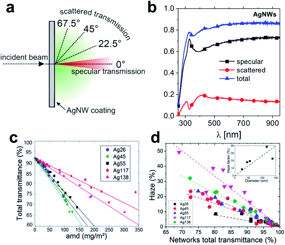 | ||
| Fig. 1 (a) Schematic of optical transmittance behaviour of NW meshes. (b) Typical spectra of specular, scattered and total transmission of light vertically incident onto AgNW mesh (NW diameter was 90 nm) (reproduced with permission. Copyright 2014, Wiley VCH Weinheim).34 (c) Experimental total transmittance values measured at λ = 550 nm of AgNW networks of different areal mass densities (amd) and composed of different types of AgNWs. (d) Experimental haze factor measured at λ = 550 nm plotted versus optical transmittance. The inset shows the increase of the haze factor with the AgNW diameter at a given optical transmittance (∼80%) (reproduced with permission. Copyright 2015, Royal Society of Chemistry).33 | ||
With increasing the length of the NWs, the percolation within a mesh at nominally identical density of NWs is statistically improved, which leads to an overall lower Rsh. As a result, potentially more conductive and simultaneously more transparent meshes are obtained in the case of higher aspect ratios of the nanowires.35 Aside from random NW mesh electrodes, there is quite a range of reports on the preparation of electrodes based on aligned NWs, which either self-assemble in dip coating processes36,37 or by using etching techniques.38 The resulting electrodes with aligned metal NWs have been shown to afford a lowered sheet resistance and a reduced roughness compared to random NW networks. Some recent approaches to prepare uniform and ordered metal nanomesh electrodes involve the use of micro- or nano-sphere lithography, which relies on an array of self-assembled polymer or silica spheres that function as a shadow mask for the deposition of a metal layer. Semi-transparent Cu nano-mesh electrodes with a sheet resistance of 17 Ω sq−1 and 80% transmittance were realized that way.39 Alternatively, ordered Cu mesh electrodes were prepared by nano-second laser ablation of a thermally evaporated Cu layer under ambient conditions.40 This way, semi-transparent (83% at 550 nm) and conductive (sheet resistance 17.5 Ω sq−1) metallic honeycomb structures were patterned into the Cu layers on top of a range of flexible substrates.
Models for the simulation of NW mesh electrodes critically rely on data about the contact/junction resistance, which strongly depends on the use of capping agents and post-treatment conditions. To reduce the contact resistance between crossing AgNWs, various approaches have been considered. Among them, “plasmonic welding” appeared to be very promising, as it showed some kind of self-limiting character.28,41 As a variant, Lu et al. proposed an approach based on a plasmon-induced chemical reaction that allowed for low-cost room-temperature selective growth of silver nano-particles around the NW junctions at light power densities as low as 5 mW cm−2.42 Thereby, Rsh was reduced from several kΩ sq−1 down to 13.4 Ω sq−1 at an almost unchanged transmittance of 88.7% at 550 nm. It has been shown that the junction resistance may be substantially altered by the use of a conductive “glue”, e.g. poly(3,4-ethylenedioxythiophene)–poly(styrene sulfonate) (PEDOT:PSS) or a conductive metal-oxide, to improve the joint between the wires (Fig. 2).43,44 This glue may at the same time improve the adhesion of the NW mesh electrode to the substrate and it will provide lateral charge transport to electrically connect the open spaces between the wires, which are typically on the order of several μm2, to the mesh. In devices using a pristine mesh electrode, the extraction/injection of charges from/into the device would otherwise be limited by the lack of lateral conductivity of the functional device layers. This states a particular issue in organic semiconductors, which typically do not provide sufficient lateral conductivity.34 The conductive filler medium does not need to provide a very high lateral conductivity itself, but it should be highly transparent, in order not to spoil the overall transmittance of the NW electrode.
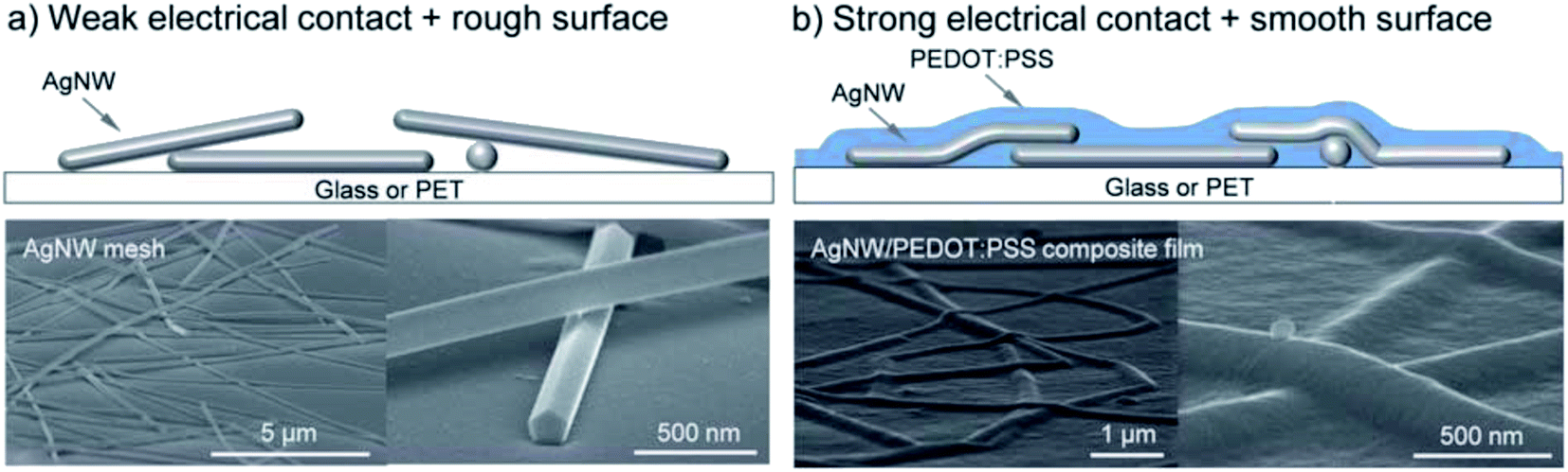 | ||
| Fig. 2 (a) Bare AgNW mesh. (b) AgNW–PEDOT:PSS composite film (reproduced with permission. Copyright 2012, Royal Society of Chemistry).31 | ||
2.2. Nano-wire based composite electrodes
A majority of reports on metallic-NW meshes as electrodes for OSCs is focussed on silver-NWs (AgNWs). AgNWs are easily processed into transparent conductive films from a range of dispersions in water or alcohol, some of which are even commercially available. Due to their high surface-to-volume ratio, pure AgNWs degrade more rapidly in an ambient atmosphere than bulk silver electrodes.45,46 Specifically, the concomitant influence of humidity and illumination on the degradation has been unravelled by Jiu et al.46 Therefore, embedding the AgNWs into a conductive matrix appears to be an avenue to mitigate these stability issues. As already mentioned above, the most straight forward approach to realize highly conductive and transparent films based on metallic NWs is to overcoat these NW meshes with conductive PEDOT:PSS. However, due to its acidic nature and its intrinsic structural inhomogeneity, PEDOT:PSS has been associated with several degradation mechanisms and a limited device lifetime.47–50 Furthermore, it has been shown that upon prolonged contact with PEDOT:PSS the electrical properties of the AgNWs deteriorated.51 As discussed later, the application of water-dispersed PEDOT:PSS is even more critical in emerging highly efficient organo-metal halide perovskite solar cells (PSCs), as the photo-active layers are subject to decomposition upon contact with moisture.52There are a number of reports on composite electrodes in which metal-NWs are combined with conductive metal-oxides. For example, Kim et al. presented a composite of a solution processed AgNW mesh sandwiched between ZnO layers prepared by magnetron sputtering.53 The resulting tri-layer electrodes provided a high optical transmittance of 92% at 550 nm and a Rsh of 8 Ω sq−1. In addition, AgNWs confined between ZnO films were found to withstand annealing temperatures up to 375 °C without melting into single disconnected Ag droplets. The tri-layers of ZnO/AgNWs/ZnO were used in CIGSSe solar cells. However, the application of this tri-layer electrode on top of organic solar cells or perovskite based devices would require additional protection measures to avoid damage of the sensitive photo-active layers during sputter deposition. Very recently, Huang et al. used Al:ZnO/AgNWs/Al:ZnO, in which they used magnetron sputtering for the deposition of the Al:ZnO. The resulting electrodes had a sheet resistance of 8.6 ohm sq−1 and a transmittance of 74.4%. Embedding the wires into the Al:ZnO afforded electrodes with a superior thermal stability compared to those based on pristine AgNWs.54
Zilberberg et al. suggested composite electrodes, where they used low temperature atomic layer deposition (ALD) to coat a AgNW mesh with Al:ZnO.34 Due to the conformal shadow-free coating principle of ALD, every NW in the mesh was individually coated and became embedded into the AZO matrix. The combination of the AgNW and the AZO matrix led to a dramatically reduced Rsh from 90 Ω sq−1 down to 31 Ω sq−1 and an average optical transmittance in the visible spectral region of 86%. A relatively high contribution of scattered transmittance (∼23%) was found, which may be favourable for light trapping in thin film PV applications. The same group also demonstrated composites of AgNWs and room-temperature sol–gel processed SnOx that resulted in a low Rsh of 5.2 Ω sq−1 along with 87% average optical transmittance. Solution processed, semi-transparent OSCs were fabricated using these hybrid AgNW/SnOx electrodes as top contacts.
In a similar sense, Song et al. used a stabilized sol–gel titanium isopropoxide solution to form a conformal amorphous TiOx capping on top of the AgNW mesh.55 Without any thermal treatment, the Rsh of the resulting hybrid electrode was significantly reduced to 13.2 Ω sq−1, while the transmittance at 550 nm was 86%. Hybrid films were thermally stressed at 200 °C for 1 h and up to 10 min at 300 °C without a significant change in electrical properties. In addition, a corrosion test was applied to TiOx coated and neat AgNWs by dipping both into aggressive sulfur solution in dimethylformamide. After 30 min, the resistance of the AgNW/TiOx hybrid doubled, whereas unprotected NWs exhibited a 6 orders of magnitude increase of Rsh.
Chen et al. demonstrated a transparent electrode of AgNWs with hot-press transferred graphene monolayers (500 psi @ 130 °C) simultaneously lowering the contact resistance between the wires and filling the gaps between the wires with conductive graphene (Rsh = 1.3 kΩ sq−1).56 This approach delivers hybrid electrodes with a Rsh of 14 Ω sq−1 combined with an optical transmittance at 550 nm of 90%. Deng et al. pushed this idea further and developed a mass production R2R line.57 There, the graphene monolayer was hot laminated at 100 °C onto a PET foil with pre-casted AgNWs at a coating speed of up to 2 cm s−1. Two touching rollers defined the lamination step temperature and provided pressure during a transfer (Fig. 3). A continuous and crack-free graphene monolayer covering the NWs was obtained, efficiently encapsulating them and thereby dramatically enhancing their corrosion stability as well as their adhesion to the substrate. An excellent combination of Rsh = 10 Ω sq−1 and transmittance of 84% at 550 nm was achieved. These characteristics did not change even after 1000 bending cycles to 20 mm curvature radius.
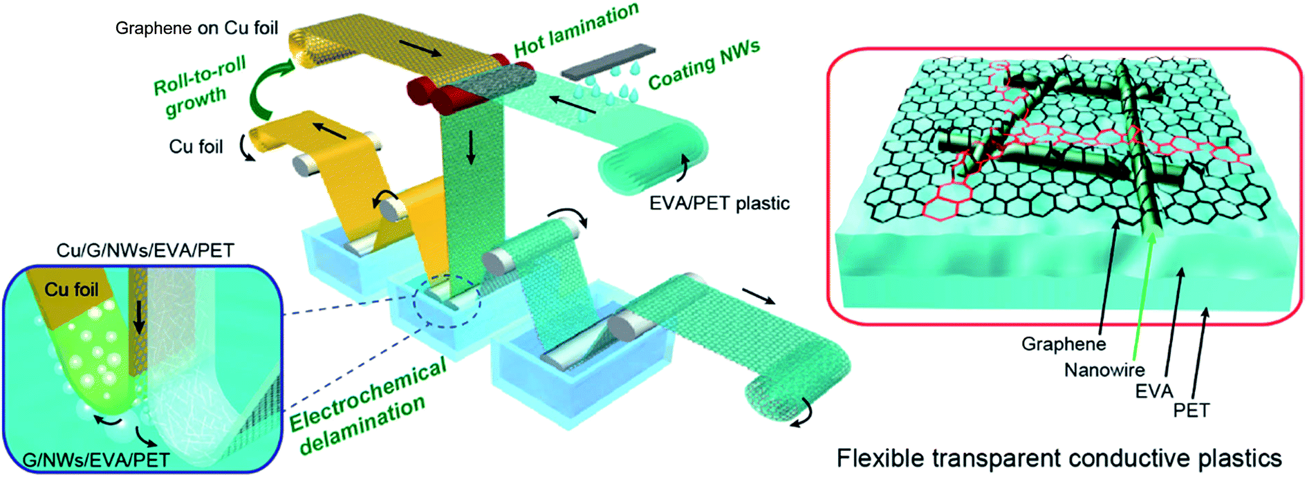 | ||
| Fig. 3 Schematic of a R2R fabrication process for large-scale transparent electrodes of AgNWs and a hot-laminated graphene monolayer (reproduced with permission. Copyright 2015, American Chemical Society).57 | ||
Due to its relatively low material cost58 and the only marginally lower specific conductivity of copper compared to silver, Cu is an excellent candidate for the mass production of (transparent) opto-electronic devices. Recently, interest in copper-NWs (CuNWs) emerged. Aspects of NW synthesis and processing of flexible and stretchable conductive films from CuNWs have been discussed in the literature.59–64 A particular issue associated with CuNWs is their susceptibility to corrosion. In an analogy to the approaches discussed for AgNWs, work to mitigate the corrosion problem suggested to cover the NWs with a shell of a more robust metal or with a metal-oxide, which significantly improved the stability of the CuNW based mesh electrodes.65–67
In a similar line of thought, Won et al. demonstrated a hybrid approach by sandwiching a CuNW mesh between two RF-sputtered AZO layers.68 Prior to deposition via transfer printing from a cellulose ester membrane, the CuNWs were treated with lactic acid to remove organic capping agents and Cu-oxide species from the surface. Thereby, additional post-annealing could be avoided. After the deposition of the AZO layer on the CuNW mesh, its Rsh reduced from 150 to 36 Ω sq−1 and the optical transmittance was 84% at 550 nm. The electrical properties of the composite remained stable for at least 5 months at RT and under ambient conditions, which implies not only a mechanical stabilization of NWs, but also some significant encapsulation of the CuNW by the AZO coating. However, an accelerated aging test at 80 °C in an ambient atmosphere resulted in doubling of Rsh after only 166 h. At elevated temperatures, the metal oxide coating becomes more permeable for moisture and oxygen from the ambient atmosphere leading to accelerated degradation of the CuNWs. In addition, for the AZO/CuNW/AZO tri-layer deposited on PET, no cracks and only a slight increase of Rsh were observed after repeated bending (1280 cycles) to 2.5 mm curvature radius.
A solution processed hybrid electrode based on Meyer-rod coated CuNWs (D 67 ± 15 nm and L 20 ± 5 μm) was demonstrated by Stewart et al.69 To remove the surface oxide and to render the mesh more conductive, the authors applied dipping into acetic acid. Protection from further corrosion was provided by introducing a Ni-capping to the CuNWs via electroless plating. The NW diameter increased to 90 ± 31 nm, which resulted in a transmittance of 80% and a Rsh of 36 Ω sq−1. The Ni capping on the CuNW mesh provided oxidation resistance comparable to AgNWs and enhanced the thermal stability. A similar concept was followed by Chen et al., who prepared oxidation-resistant Cu–Ni core–shell nanowires, which afforded solution processed transparent conductive layers with a transmittance of 76% and a sheet resistance of 300 Ω sq−1.70
A fast route to remove the surface oxide and organic residues from the CuNW mesh by sintering via pulsed xenon light (2393 J cm−2) was proposed by Ding et al.71 Thus, CuNW (D 40 nm and L 50 μm) networks with 22.9 Ω sq−1 and 81.8% transmittance resulted after only 6 ms exposure to light without any additional chemical treatment. Similarly, Zhong et al. used intense light irradiation to remove the polyvinylpyrrolidone capping agents from the CuNW to form semi-transparent electrodes with Rsh = 24.5 Ω sq−1 and an average transmittance of 83%.72
Kim et al. demonstrated a transparent conductive hybrid comprising mesoscale hexagonal copper mesh structures (Fig. 4).73 For this, a high quality non-oxidized and well-adhering copper layer (∼60 nm) was first RF-sputtered from a Cu target onto a polyimide substrate and then wet-etched using a photoresist mask. Covering these structures (1 μm line width and 30 μm hexagonal diameter) with RF-sputtered ZnO or AZO delivered high performance composites with a transmittance greater than 90% at 550 nm and Rsh of 7.7 and 6.2 Ω sq−1, respectively. These numbers remained rather stable up to 150 °C in ambient air. Bending to a curvature radius of 2 mm for 1000 times increased Rsh by only 8%.
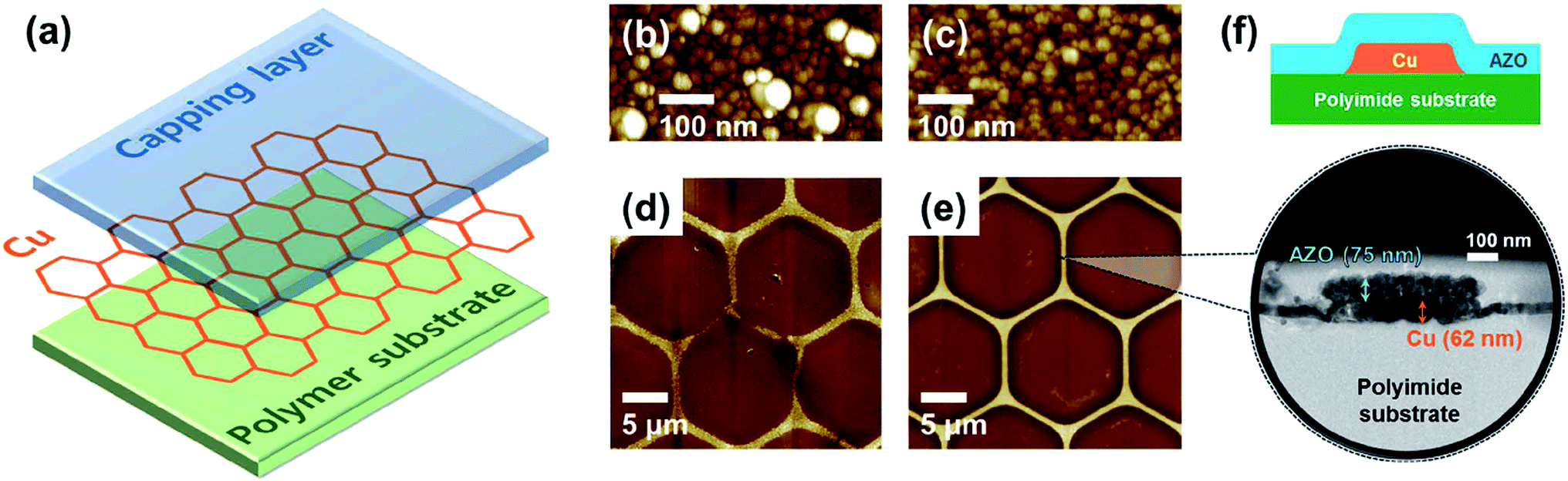 | ||
| Fig. 4 (a) Structure of the Cu mesh hybrid electrode. (b and c) AFM topography images of Cu thin films on polyimide substrates fabricated using a polycrystalline Cu target and a single-crystal Cu target, respectively. (d and e) AFM topography images of Cu mesh electrodes fabricated by wet etching using the two types of Cu thin films in (b) and (c), respectively. (f) Illustration and HRTEM image of the cross-sectional structure of a Cu mesh hybrid electrode with Al:ZnO as the capping layer and polyimide as the polymer substrate (reproduced with permission. Copyright 2015, American Chemical Society).73 | ||
Self-organized cracking patterns in a range of sacrificial-layer materials have been used as a shadow mask for the subsequent deposition of several metal thin-films.74 After lift-off, a semi-transparent mesh-electrode based on a nm-sized metallic backbone resulted with a sheet resistance as low as 0.5 Ω sq−1 and a concomitant transmittance of about 83%.75 The open spaces in the electrode have been bridged using moderately conductive ZnO or PEDOT:PSS.76,77 The technique has been demonstrated to be up-scaled and it can also be applied to create top electrodes in solar cells.
Semi-transparent Cu-mesh electrodes based on ordered pore arrays were demonstrated by Zhou et al.78 They prepared these well-ordered structures by using self-organized porous honeycomb patterns that evolve as breadth figures in PS-b-PAA on top of a Cu layer as a wet etching mask. Optimized Cu mesh electrodes had a sheet resistance of 28.7 Ω sq−1 at a transparency of 83.5%. The resulting electrodes were coated with PEDOT:PSS and they were applied in organic solar cells.
Kholmanov et al. added graphene oxide (with a sheet resistance of 36.6 ± 4.7 kΩ sq−1) via a dry transfer method onto a not-yet conductive mesh of spray-coated CuNWs.79 After annealing at 180 °C for 30 min in an Ar/H2 environment, composite films exhibited 80% optical transmittance at 550 nm and a Rsh of 34 ± 2.6 Ω sq−1. Graphene oxide did not only enhance the electrical properties of the composite film, but also provided protection for the CuNW against corrosion. Composite films did not show changes in Rsh after 72 h at 60 °C in an ambient environment, whereas the Rsh of non-protected CuNW meshes increased from initially ∼59 Ω sq−1 to ∼100 Ω sq−1. Raman spectroscopy revealed the formation of copper oxides and hydroxides upon annealing in humid air as a reason for the degradation.
Zhu et al. also used spray-coated and thermally reduced graphene oxide to improve the characteristics of CuNW meshes to 84% transmittance at 550 nm and Rsh of 21.7 Ω sq−1.80 The composite films withstood 80 °C at 80% rH for 2 days; however, they exhibited 30% increased Rsh after 30 days in an ambient environment. The same group transfer-printed the spray-coated CuNW mesh into PEDOT:PSS on PET ending up with a transmittance of 84.2% at 550 nm and a Rsh of 25 Ω sq−1.80 Bending this hybrid electrode to 5 cm radius for 400 cycles led to only 22% increase of Rsh. Chen and co-workers embedded CuNWs into a pre-deposited PEDOT:PSS layer and achieved electrodes on PET with a sheet resistance of 15 Ω sq−1 and a transmittance of 76% (at λ = 550 nm).81 Moreover, embedding the CuNW in PEDOT:PSS lowered the roughness of the resulting electrodes and substantially improved their stability against oxidation.
A CuNW–graphene core–shell electrode has been synthesized using a plasma-enhanced chemical vapor deposition process at temperatures of 400 °C.82 The resulting electrode was stable against thermal oxidation because of the impermeable graphene shells. These electrodes have been successfully applied in OSCs. It has to be noted that the elevated processing temperatures will not allow the deposition on plastic foils. Dou and co-workers reported a low temperature solution-based approach to wrap graphene oxide (GO) nano-sheets on the surface of ultrathin copper nanowires.83 The resulting electrodes based on these core–shell NWs were stable over 200 days in ambient air. Their sheet resistance (28 Ω sq−1) and transmittance of 90% were on a par with those of ITO and AgNW based electrodes.
Considering the high cost of gold, gold NWs (AuNWs) at a first glance appear less attractive than their Ag or Cu based analogues. However, the unique mechanical and optical properties of Au along with its elevated chemical stability render AuNWs a field of emerging interest. Typically, the as-synthesized AuNWs carry an insulating cap of oleylamine, which required thermal annealing or even an additional plasma (Ar/H2) treatment to provide enhanced conductivity in an AuNW mesh.84 Meanwhile, AuNWs can be synthesized with a diameter of less than 2 nm at an aspect ratio of 10![[thin space (1/6-em)]](https://www.rsc.org/images/entities/char_2009.gif) 000. This is attractive not only to allow for hybrid transparent conductive coatings with very low optical haze, but also for the creation of well-defined self-assembled NW-meshes. As an example, Maurer et al. demonstrated the self-assembly of AuNWs during the drying within voids of a nano-patterned PDMS stamp.85 With this technique, an average transmittance of neat AuNW meshes of 90% with a sheet resistance of 227 Ω sq−1 has been achieved. In a similar manner, a slower and less controlled but more simple self-assembly of AuNWs into essentially similar meshes was demonstrated by Gong et al.86 The AuNW dispersion, drop-casted onto a water surface, underwent aging in the ambient atmosphere, during which the insulating oleylamine capping of AuNWs was gradually removed by natural oxidation allowing for gradual NW alignment and mesh formation. Subsequently, the mesh was transferred onto a substrate and exhibited 92% transmittance and a Rsh of 130 Ω sq−1.
000. This is attractive not only to allow for hybrid transparent conductive coatings with very low optical haze, but also for the creation of well-defined self-assembled NW-meshes. As an example, Maurer et al. demonstrated the self-assembly of AuNWs during the drying within voids of a nano-patterned PDMS stamp.85 With this technique, an average transmittance of neat AuNW meshes of 90% with a sheet resistance of 227 Ω sq−1 has been achieved. In a similar manner, a slower and less controlled but more simple self-assembly of AuNWs into essentially similar meshes was demonstrated by Gong et al.86 The AuNW dispersion, drop-casted onto a water surface, underwent aging in the ambient atmosphere, during which the insulating oleylamine capping of AuNWs was gradually removed by natural oxidation allowing for gradual NW alignment and mesh formation. Subsequently, the mesh was transferred onto a substrate and exhibited 92% transmittance and a Rsh of 130 Ω sq−1.
As of yet, no work on composite electrodes based on AuNWs has been reported. The combination of such meshes with e.g. metal oxides or graphene coatings may have great potential for robust and optically well-defined highly transparent electrodes.
A selection of recent reports of hybrid transparent electrodes comprising metallic NW meshes is summarized in Table 1. This table also contains figure-of-merit (FOM) data calculated for composite films according to Haacke as  .87 As many authors specify the transmittance at a certain wavelength (e.g. 550 nm), we decided to use the transmittance at 550 nm for the calculation of the FOM for all NW electrodes presented in Table 1. However, caution is advised when using the FOM to compare electrodes, as the transmittance at 550 nm is not representative for the entire spectral range relevant for solar applications. In the worst case, the electrode could show a very narrow transmittance window optimized around a certain wavelength, which would then result in a high FOM, while the average transmittance might be low. Furthermore, the value of transmittance provided by different authors may vary depending on whether it is referenced to air or to some substrates (glass, PET, etc.). In particular, transmittance numbers as high as or even higher than that of a plain substrate have to be taken with care.
| Electrode structure | Average wire geometry | Deposition and (post-)treatment | Electrical and optical properties | Environmental and thermal stability | Adhesion and flexibility | Ref. and year |
|---|---|---|---|---|---|---|
| AgNWs/graphene monolayer | D 100 nm | NWs as spin-coated from IPA dispersion; graphene hot-pressed at 500 psi and 130 °C | T 550 nm = 90% | No data | No data | 56 and 2013 |
| L 20–40 μm | R sh = 14 Ω sq−1 | |||||
| Haze = 3.8% | ||||||
| FOM = 0.025 Ω−1 | ||||||
| ZnO/AgNWs/ZnO | No data | NWs spin-coated from dispersion (solvent unspecified), ZnO sputtered | T 550 nm = 92% | Up to 375 °C | 3 mm curvature | 53 and 2013 |
| R sh = 8 Ω sq−1 | ||||||
| FOM = 0.054 Ω−1 | ||||||
| AgNWs/AZO | D 90 nm | NWs as spin-coated from IPA dispersion; ZnO via ALD @ 100 °C | T av = 86% | Withstands climate cabinet 80 °C @ 80% rH for 7 days | Withstands a peeling test | 34 and 2014 |
| L > 20 μm | R sh = 31 Ω sq−1 | |||||
| Haze = 23% | ||||||
| FOM = 0.007 Ω−1 | ||||||
| AgNWs/SnOx | D 90 nm | NWs as spin-coated from IPA dispersion; SnOx sol–gel88 spin-coated @ room-temperature | T av = 87% | Withstands climate cabinet 80 °C @ 80% rH for 7 days | Withstands a peeling test | 34 and 2014 |
| L > 20 μm | R sh = 5.2 Ω sq−1 | |||||
| Haze = 19% | ||||||
| FOM = 0.048 Ω−1 | ||||||
| PET/AgNWs/ZnO | D 35 nm | NWs ink and ZnO-NPs dispersed in acetone large-area coated via rotary screen printing with drying time <30 s at 140 °C | T av > 80% | Composite exhibits 10% less transmittance and increased Rsh of 30 Ω sq−1 after 4 months in N2 | No data | 89 and 2015 |
| L 25 μm | R sh = 10–20 Ω sq−1 | |||||
| FOM = 0.010–0.005 Ω−1 | ||||||
| AgNWs/Al2O3/ZnO | No data | NWs Mayer rod coated and post-annealed 150 °C @ 3 min, then dipped into DI water for 10 min and again annealed at 165 °C @ 8 min; Al2O3 thin film via ALD @ 100 °C followed by ZnO via ALD @ 100 °C | T 550 nm > 87% | 300 °C | Over-coated with polyimide and peeled off the substrate, withstands 5000 bending cycles to 3 mm radius | 90 and 2015 |
| R sh = 10 Ω sq−1 | ||||||
| FOM = 0.025 Ω−1 | ||||||
| Polyimide/AZO/AgNW/AZO | D 75 nm | Both, top and bottom AZO RF-sputtered at 200 °C; NWs rod-coated from ethanol dispersion and dried for 3 min @ 60 °C | T 550 nm = 74.4% | 1 h @ 250 °C | Continuous increase of Rsh and crack building in AZO upon bending; an 8-fold and 14-fold increase of Rsh after 500 cycles outer and inner bending correspondingly. Withstands tape peeling test | 54 and 2015 |
| L 12 μm | R sh = 8.6 Ω sq−1 | |||||
| FOM = 0.006 Ω−1 | ||||||
| AgNWs/MoOx | D 35 nm | NWs bar-coated from ethanol dispersion at 50 °C substrate; MoOx spin-coated from ammonium heptamolybdate solution in deionized water and annealed at 100 °C | T av > 90% | No data | Tensile bending to 3 mm radius for 3000 cycles; Rsh doubled after the 1st tape peeling test, low adhesion | 91 and 2015 |
| L 15 μm | R sh = 29.8 Ω sq−1 | |||||
| Haze = 0.9% | ||||||
| FOM = 0.012 Ω−1 | ||||||
| AgNWs/TiOx | D 90 nm | NWs spin-coated from ethanol dispersion; sol–gel TiOx spin-coated from titanium isopropoxide solution in ethanol and ethanolamine; 80 °C @ 5 min baked for solvent evaporation | T 550 nm = 86% | 300 °C @ <10 min or 200 °C @ >1 h; extended protection against AgNW sulfurization while dipped into sulfur-DMF | Withstands tape peeling test, withstands 500 cycles bending to 5 mm radius | 55 and 2015 |
| L 30 μm | R sh = 13.2 Ω sq−1 | |||||
| FOM = 0.017 Ω−1 | ||||||
| PET/AgNWs/graphene monolayer | D 35 nm | AgNWs coated onto PET via Mayer rod; graphene R2R hot-laminated @ 100 °C onto NWs from a copper foil | T 550 nm = 84% | 60 days in ambient atmosphere @ RT | 10000 bending cycles to 20 mm radius; withstands >100 tape peeling cycles |
57 and 2015 |
| R sh = 10 Ω sq−1 | ||||||
| FOM = 0.017 Ω−1 | ||||||
| AgNWs/SnOx | D 125–250 nm | PVP coating of NWs is washed off and replaced by SnO2 NPs; a hybrid film is blade-coated at RT in a single step from a mixed dispersion of AgNWs and SnO2 with addition of ammonia | T 550 nm = 84% | No data | No data | 92 and 2016 |
| L 15–65 μm | R sh = 11 Ω sq−1 | |||||
| FOM = 0.016 Ω−1 | ||||||
| CuNWs/reduced graphene oxide | D < 60 nm | NWs spray-coated from a dispersion in IPA and hydrazine monohydrate and annealed 180 °C @ 30 min in Ar/H2 environment; graphene oxide dry transferred onto mesh from PMMA substrate | T 550 nm = 80% | No change of Rsh at 60 °C in ambient air for 72 h | Survives dipping into HCl; no delamination of composite in KCl | 79 and 2013 |
| L > 20 μm | R sh = 34 ± 2.6 Ω sq−1 | |||||
| FOM = 0.003 Ω−1 | ||||||
| AZO/CuNWs/AZO | D 66 nm | NWs dispersed in IPA, treated with lactic acid and transfer printed onto substrate, vacuum-dried; AZO layers are magnetron sputtered w/o post-annealing | T 550 nm = 84% | Stable >5 month at RT; Rsh doubles after 166 h @ 80 °C | Deposited on PET, remains stable after 1280 bending cycles to 2.5 mm curvature radius, no cracks in AZO visible | 68 and 2014 |
| R sh = 36 Ω sq−1 | ||||||
| L > 50 μm | FOM = 0.005 Ω−1 | |||||
| Cu-mesh/ZnO | Hexagonal structures with 1 μm line width and 30 μm diameter | 62 nm thick Cu-films RF-sputtered from a single-crystalline target at 150 °C, lithographically patterned and covered with RF-sputtered metal oxide at 150 °C | T 550 nm = 90% | R sh rather stable up to 150 °C | 1000 bending cycles to 2 mm radius leads to 8% Rsh increase | 93 and 2015 |
| R sh = 7.7 Ω sq−1 | ||||||
| FOM = 0.045/Ω−1 | ||||||
| Cu-mesh/AZO | T 550 nm = 90% | |||||
| R sh = 6.2 Ω sq−1 | ||||||
| FOM = 0.056 Ω−1 | ||||||
| PET/PEDOT:PSS/CuNWs | D 50 nm | 100 nm PEDOT:PSS pre-coated on substrate, CuNW spray coated on top, subsequently annealing at 140 °C for 3 min and pressing at 20 MPa for 10 s | T 550 nm = 76% | Stable upon exposure to air | No data | 81 and 2015 |
| L 20–30 μm | R sh = 15 Ω sq−1 | |||||
| FOM = 0.0042 Ω−1 | ||||||
| PET/CuNWs/PEDOT:PSS | D 45 nm | Spray-coated from IPA dispersion onto 60 °C glass, plasma-treated with <5 torr air-plasma and transfer-printed onto PEDOT:PSS on PET | T 550 nm = 84.2% | No data | Bending 400 cycles to 5 cm radius leads to 22% increase of Rsh | 80 and 2015 |
| L 75 μm | R sh = 25 Ω sq−1 | |||||
| Haze = 6% | ||||||
| FOM = 0.007 Ω−1 | ||||||
| CuNWs/reduced graphene oxide | D 45 nm | Spray-coated from IPA dispersion onto 60 °C glass, plasma-treated with <5 torr air-plasma and covered with graphene oxide IPA dispersion; annealed 1 h @ 200 °C | T 550 nm = 84% | 2 days @ 80 °C and 80% rH doesn't change Rsh; 30 days @ ambient air increases Rsh by 30% | No data | 80 and 2015 |
| L 75 μm | R sh = 21.7 Ω sq−1 | |||||
| Haze = 6% | ||||||
| FOM = 0.008 Ω−1 | ||||||
| CuNWs/graphene oxide | D 17 nm | CuNWs wrapped by graphene oxide of 1 to 5 nm thickness in methanol and diluted with IPA; deposition via filtration method with subsequent transfer onto glass, annealed at 260 °C under Ar/H2 | T 550 nm = 90% | Damage to NW at >260 °C; stable for at least 50 h @ 80 °C @ 40% rH in air or 200 days at room temperature | No data | 83 and 2016 |
| R sh = 28 Ω sq−1 | ||||||
| Haze = 2% | ||||||
| FOM = 0.012 Ω−1 |
2.3. Application of nano-wire based electrodes in thin-film solar cells
Lu and co-workers demonstrated a “plasmonically treated” AgNW mesh as an electrode in organic solar cells. To this end, the mesh was lifted off from a glass substrate in water and transferred to a PET/PDMS substrate, and subsequently it was over-coated with PEDOT:PSS.42 Afterwards, the entire electrode stack was hot-laminated onto a bulk heterojunction solar cell stack. The resulting devices delivered the same fill factor (FF) and open circuit voltage (Voc) as reference devices with an opaque metal electrode.Kang et al. made use of R2R compatible capillary printing (Fig. 5) to prepare highly aligned AgNW (D 32 nm and L 25 μm) films with low surface roughness for opto-electronic applications.94 By dragging the NWs by a nano-patterned PDMS stamp introducing meniscus surface tensions, the authors claim to achieve a lower percolation threshold compared to stochastic NW meshes and therefore obtain a higher optical transmittance 96.7% compared to stochastic meshes (92.9%) at the nearly same Rsh of 19.5 Ω sq−1. In addition, 2.4 times lower haze was achieved for films with uni-directionally aligned NWs compared to random meshes. As a bottom electrode in OSCs, capillary printed aligned NWs (covered with PEDOT:PSS) allowed for a higher short circuit current (Jsc) compared to devices based on random AgNW meshes. The cells retained 80% of their initial power conversion efficiency (PCE) after 1000 bending cycles to 5 mm curvature.
 | ||
| Fig. 5 Solution-printed highly aligned AgNW arrays. (a) Schematic of the capillary printing process using a nano-patterned PDMS stamp to produce highly aligned AgNW arrays. (b) Schematic showing the alignment process during capillary printing of unidirectional AgNW arrays. The solvent-evaporation-induced capillary force produces highly aligned networks by dragging confined AgNWs at the solid–liquid–vapour contact line. (c) Dark-field optical images of differently oriented AgNW structures fabricated with a solution concentration of 0.05 wt% via one-step (unidirectional) and multistep (45°, 60°, and 90° crossed) capillary alignments. The scale bar is 40 μm. The fast Fourier transform (FFT) analyses of the images, presented in the insets, show the corresponding geometric structures (reproduced with permission. Copyright 2015, American Chemical Society).94 | ||
Flexible OSCs comprising AgNW (D 45 nm and L 40 μm)/PEDOT:PSS transparent bottom electrodes (84.5% average transmittance at 16.2 Ω sq−1) that were bar-coated on PET modified with an acrylic resin were shown by Wang et al.95 During the post-annealing step of the NW electrodes at 80 °C, the NWs were sinking into the resin layer, which reduced the roughness of the electrode. A low roughness of the bottom electrode is essential in order to avoid short circuits in the cells. Devices exhibited a 32% higher PCE compared to devices on glass/ITO. The improvement was shown to originate from plasmonic scattering effects due to the AgNWs (Fig. 6). After 60 bending cycles, only negligible variations in device performance were observed. Moreover, the adhesion of the electrode was tested by applying a tape peeling test up to 20 times with a negligible change in Rsh.
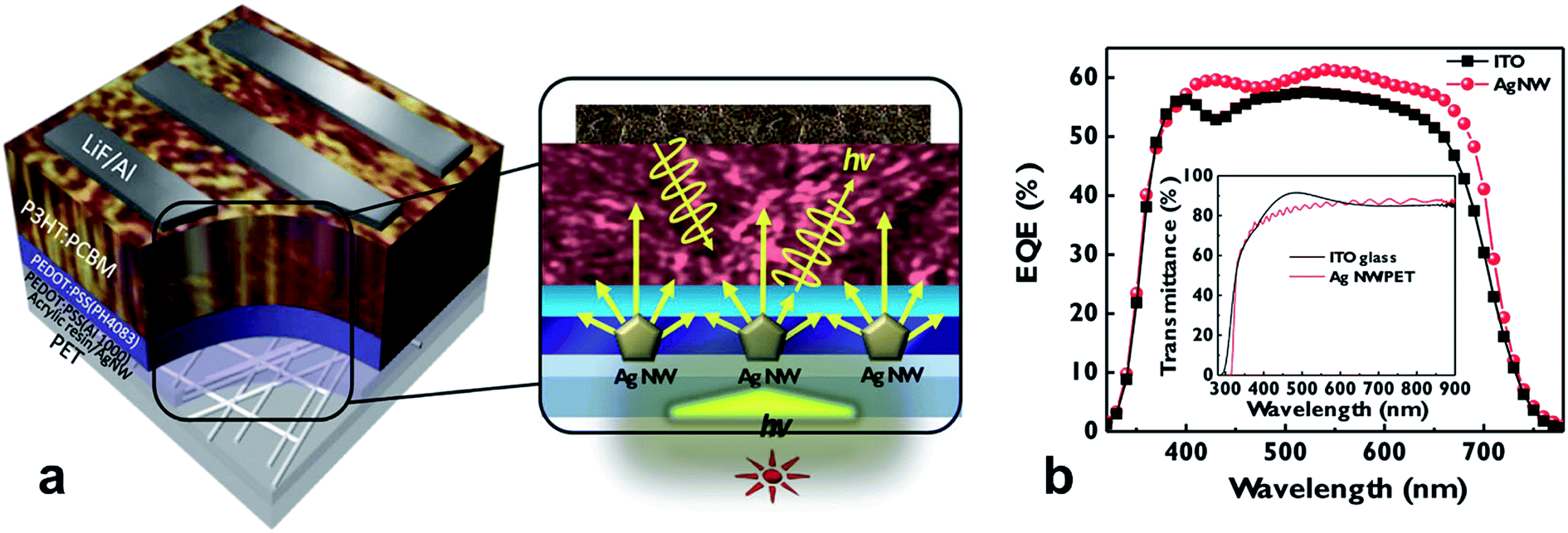 | ||
| Fig. 6 (a) Schematic illustration of light scattering and trapping phenomena induced by the AgNW mesh in the device; (b) external quantum efficiency (EQE) spectra of a P3HT:PCBM OSC with the AgNW mesh electrode and the reference device with ITO; the inset depicts transmittance spectra of corresponding electrodes (reproduced with permission. Copyright 2015, Wiley VCH Weinheim).95 | ||
Angmo et al. used a rotary screen printing setup to fabricate homogeneous large-area AgNW meshes covered with ZnO.89 An efficient in situ planarization of NW meshes resulted from the process specific shear forces during the coating of the NW mesh. Only a very short drying step (140 °C for less than 30 s) was applied, which allowed for coating speeds of 10–20 m min−1. The resulting films on PET foil exhibited a uniform transmittance of 84% in the range of 550–800 nm and a Rsh of only 10–20 Ω sq−1. Large-area OSCs on PET foil using this composite as a bottom electrode demonstrated very high Jsc and fill factor (FF) that hint to simultaneous high transparency and efficient lateral transport of photo-generated charges.
Bob et al. demonstrated a nanocomposite film comprising AgNWs and SnO2 NPs deposited in a single step by blade coating.92 Without post-treatment, a low Rsh of 11 Ω sq−1 with corresponding T550 nm of 84% resulted. Although the obtained films were macroscopically well-conductive, their application on top of thin-film a-Si solar cells led to poor device fill factors (31%). Only after introduction of a layer of moderately conductive AZO between a-Si and the AgNW/SnO2 electrode the fill factor increased to 65%. The AZO was claimed to be necessary for the formation of an ohmic contact to the silicon photo-active layer.
So-called “multi-length scale AgNW grid electrodes” were demonstrated by Wu et al.96 The grids were prepared by patterning a mesh of AgNWs by etching in I2 vapor. ZnO nanoparticles were used as conductive fillers, which provided the necessary lateral charge collection over distances of 20 μm. Devices with a PCE of >9% were achieved, comparable to that based on traditional ITO electrodes.
Compared to AgNW based electrodes, the field of CuNWs as a platform for electrodes in thin film solar cells is far more limited. Among the few reports, CuNiNW meshes covered with PEDOT:PSS were utilized as a bottom transparent electrode in opaque OSCs and led to very similar device characteristics to AgNW/PEDOT:PSS-based counterparts. However, somewhat lower Voc, Jsc and FF were achieved in comparison with those of ITO-based devices.69 Won et al. embedded CuNWs into Al-doped ZnO (AZO), which dramatically improved the thermal stability and oxidation resistance of the CuNWs.97 The AZO/CuNW/AZO composite electrodes had a high transmittance of 83.9% at 550 nm and sheet resistance 35.9 Ω sq−1. These electrodes were used in Cu(In1−x,Gax)(S,Se)2 thin-film solar cells with a performance comparable to that of ITO-based analogues.
Solar cells based on organo-lead halide perovskites have seen tremendous progress over the past five years.98 Their power conversion efficiency (PCE) has skyrocketed to reach a level of >20%.99 For a general introduction to this field the reader is referred to some very recent review articles.100,101 The application of perovskites in semi-transparent cells for building integrated photovoltaics102 or in tandem architectures with a single crystalline silicon or Cu(In,Ga)(Se,S)2 (CIGS) cell to unlock efficiency levels of 30% is currently pursued.103–106 All of these designs rely on highly efficient, versatile, yet cost effective transparent electrodes as essential building blocks. Concerns about intrinsic and extrinsic stability are still intimately linked to perovskite photovoltaic technology.52,107,108 As an example, perovskites like CH3NH3PbI3 decompose to their constituents, i.e. HI, CH3NH2 and PbI2, in the presence of water.109 On top of this, the intrinsic decomposition of CH3NH3PbI3 to CH3NH3I and PbI2, which is thermally activated, occurs even under inert conditions.110,111 Secondary effects of perovskite decomposition have to be considered, such as the degradation of functional building blocks in the solar cell due to the corrosive effect of the perovskite decomposition products, like HI or CH3NH3I. Specifically, the corrosion of metal electrodes like Ag or Al has been identified to be a critical issue.112–114
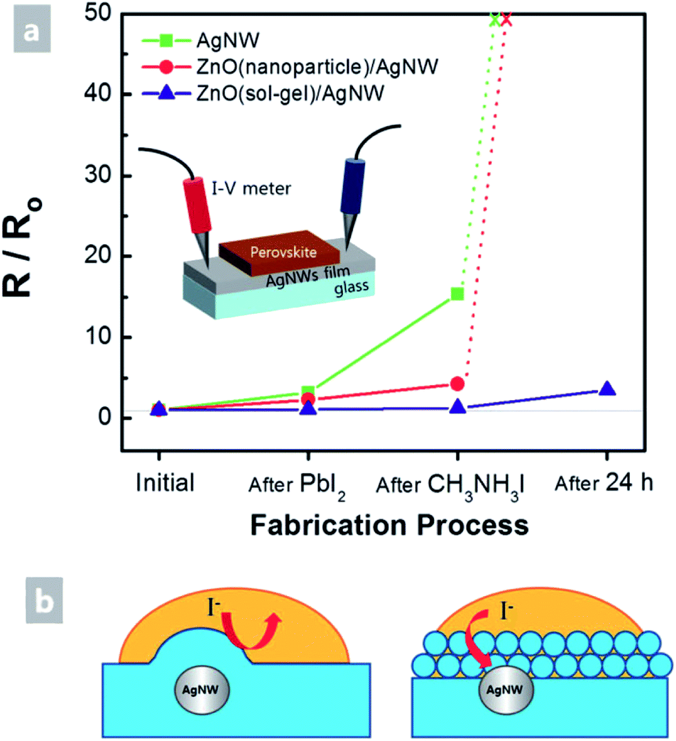
Corrosion of metal-electrodes in perovskite cells is of particular importance if the metal is part of the bottom electrode, onto which the perovskite layer is formed from a precursor solution, i.e. CH3NH3I and PbI2 in dimethylformamide. Bush et al. reported on corrosion issues when AgNWs were used as the bottom electrode in perovskite solar cells, due to the formation of AgI, which spoiled the conductivity of the electrode.115 In the work of Kim et al., the conductivity of an AgNW electrode has been shown to rapidly degrade upon exposure to CH3NH3I (Fig. 7).116 They were using a coating of either ZnO nanoparticles or sol–gel derived ZnO. The sol–gel ZnO has been found to form a rather dense protection for the AgNW, which prevented the chemical attack due to the CH3NH3I. In Fig. 7b the different permeability of the sol–gel or nanoparticle based ZnO coating for iodine compounds (denoted as I−) is visualized.
 | ||
| Fig. 7 (a) Resistance changes in AgNW films and ZnO/AgNW films during sequential perovskite deposition. After 24 h of aging, resistances were re-measured. (b) Schematics showing cross-sections of composite electrodes when the perovskite precursor solution containing iodine ions was coated on either the AgNW-sol–gel-derived (left) dense composite electrode or the AgNW-nano-particulate porous (right) composite electrode (reproduced with permission. Copyright 2016, Royal Society of Chemistry).116 | ||
Han et al. combined AgNW (D 100–150 nm and L 60 μm) meshes on PET foil with pulsed-laser-deposited F:ZnO while keeping the substrate at room temperature.117 The resulting hybrid electrode with a T550 nm of 83% and haze of 36.5% (Rsh = 17 Ω sq−1) was applied as a bottom transparent electrode in perovskite solar cells. Remarkably, due to the high transmittance and increased haze, devices based on hybrid AgNW/F:ZnO electrodes outperformed that based on commercial F:SnO2. The composite electrode on a PET foil remained stable even after 1000 bending cycles to 5 mm curvature radius.
Kim et al. introduced their concept of AgNW-based composite bottom electrodes for perovskite solar cells comprising an all-solution-processed sandwich structure ITO/AgNWs/ITO/ZnO.116 The ITO/ZnO double layer was claimed to prevent diffusion of halogen species that might corrode the silver wires. The resulting electrodes exhibited 79.5% optical transmittance at 550 nm and Rsh of 18 Ω sq−1. Perovskite solar cells based on this composite bottom electrode exhibited lower Jsc and FF compared to reference devices based on more transparent and conductive commercial F:SnO2.
A number of papers reported the use of a NW mesh as a semi-transparent electrode on top of a perovskite solar cell. For example, Guo et al. showed the so-called inverted perovskite cells (in contrast to OSCs, in this case, the top electrode is the cathode). They introduced a uniform ZnO nanoparticle layer between the electron conduction layer (PCBM) and spray-coated AgNW (L 30 μm and D 30 nm) mesh.118 Due to its low WF, ZnO ensured a good ohmic contact with PCBM and simultaneously allowed for an improved device shunt-resistance. However, compared to reference devices comprising ZnO/opaque metal electrodes, devices with AgNW-based transparent electrodes exhibited lower fill factors (66.8% vs. 71.9%) and 5 times higher series resistance. For these devices, the authors report a very poor stability, even if stored in nitrogen. They suggested that the degradation was due to diffusion of iodine based products which were not sufficiently blocked by the ZnO-NP layer, and which led to the formation of insulating AgI on the surface of the AgNWs. A similar approach with AgNWs spray-coated from an IPA dispersion onto a solution processed ZnO-NP film on top of a perovskite solar cell was demonstrated by Quiroz et al.119 Perovskite solar cells with 37% average visible transmittance (AVT) and an efficiency of 7.8% were achieved. The authors did not comment on the stability issues encountered in other reports. Chang et al. demonstrated semi-transparent perovskite solar cells using semi-transparent top electrodes of AgNWs (L 25 μm and D 70 nm).120 Specifically, they employed a ZnO electron extraction layer deposited by ALD directly on top of the perovskite, which they found to allow for better electron extraction compared to a ZnO layer formed from a nanoparticle dispersion. The AgNW mesh on top of the ZnO was sealed by a 50 nm ALD Al2O3-based encapsulation layer, which formed an excellent gas permeation barrier (Fig. 8a). Thereby, semi-transparent perovskite solar cells with an average transmittance of 25.5% and a PCE of 10.8% were achieved, which showed outstanding stability in ambient air (Fig. 8b).
 | ||
| Fig. 8 (a) Layer sequence of semi-transparent perovskite cells based on AgNW sandwiches between ZnO and Al2O3 deposited by ALD. (b) Stability of the PCE upon storage in an ambient atmosphere (30 °C @ 65% rH). Device C is an opaque reference device with ALD-ZnO/thermally evaporated Ag top contact; device D – ALD-ZnO/AgNW semitransparent device w/o Al2O3 encapsulation; device F – ALD-ZnO/AgNW semitransparent device with ALD-Al2O3 encapsulation (reproduced with permission. Copyright 2015, American Chemical Society).120 | ||
3. Transparent electrodes based on ultra-thin metal layers (2D)
It is well known that thin metal layers with a nominal thickness of about 10 nm can be simultaneously conductive and semi-transparent. The most frequently used metals for semi-transparent electrodes are Ag, Cu, Au and Al. They are known for their intrinsically high electrical conductivity in the bulk, which ranges between 1.6 and 2.8 μΩ cm.121 At the same time, they are fairly easily processed as thin films, e.g. by thermal evaporation or sputter deposition techniques. It has to be noted though that the required thickness-control on the nanometer scale infers particular challenges for large area applications of ultra-thin metal layers.3.1. Growth of thin metal films
While the conductivity of ideal ultra-thin metal layers can be modelled within the Fuchs–Sondheimer theory,122,123 it has to be kept in mind that, unfortunately, the deposition of thin metal films on a wide range of surfaces results in nanometer sized island-like patterns rather than continuous layers. Below the percolation threshold, the metal islands are separated and the layer has a low conductivity. With increasing the amount of deposited metal, the conductivity increases by orders of magnitude once the percolation threshold is reached.124 For the application as a transparent electrode, the metal layer must therefore be sufficiently thick to reach percolation but at the same time it must be as thin as possible to achieve a high optical transmittance.To improve the wettability of the metal layer, and thereby to lower the equivalent mass per area of metal required to reach the threshold of percolation, several approaches have been considered. For example, a thin nucleation layer (typical thickness: 0.1–1 nm) of aluminum,125–127 chromium,128 copper,129 germanium,130,131 nickel,132 niobium,133 tin,134 titanium,135 or tungsten136 has been used for surface functionalization before deposition of the actual Ag or Au ultra-thin-film. Poly(3,4-ethylene dioxythiophene):poly(styrene sulfonate) (PEDOT:PSS)137 as a solution processed nucleation layer has also been considered. Very recently, a 100 nm thick layer of the polymer resin SU-8 spin coated on top of a glass substrate has been shown to promote the percolation of a thermally evaporated Au layer by the formation of chemical bonds between Au and the SU-8 film.138
In general, when adhesion layers are used, care must be taken, to avoid or at least to minimize parasitic optical absorption due to the nucleation layer itself. Moreover, the nucleation layer may significantly alter the plasmonic properties of the resulting metal thin-film,139 which has to be taken into account in the modelling of electrode and device architectures. Self-assembled monolayers (SAMs), e.g. (3-mercaptopropyl)trimethoxysilane or (3-aminopropyl)trimethoxysilane, were applied for surface functionalization to improve the growth, adhesion and percolation of ultra-thin metal layers, without detrimental impact on the optical/plasmonic properties of the resulting metal layers.139–142
A further concept to facilitate percolation in ultra-thin metal films is to use alloys instead of pristine metals. Alloying Ag with about 4–10% of Al suppressed the formation of 3D islands and afforded smooth, highly conductive layers with a thickness as low as 6 nm.144,145 Alternatively, some slight oxidation of the Ag and the formation of about 4% of AgOx during sputter deposition of the metal layer by adding oxygen to the sputter gas have been evidenced to reduce island formation and enabled the preparation of highly conductive layers with a thickness of 6 nm.146 By a similar token, smooth, percolated, Cu layers with a thickness of only 2.5 nm were achieved by incorporating some oxygen (typ. 5–6%) into the sputter atmosphere, whereas pure Cu layers required a nominal thickness of about 5 nm to reach percolation (Fig. 9). The (weak) oxidation of the Cu at the nucleation stage was argued to prevent surface migration of the Cu and thereby suppressed island growth.143 Surprisingly, the oxygen incorporation seemingly did not deteriorate the electrical conductivity. Later, the same group showed that nitrogen could be as well incorporated into the Cu layer with a similar beneficial effect on the morphology.147
 | ||
| Fig. 9 Highly magnified field-emission scanning electron microscopy images showing the coalescence behavior of (a–d) Cu and (e–h) Cu(O = 5.0%) clusters with low thicknesses (1.5–5.0 nm) deposited on ZnO films during the very early stages of growth. Scale bar, 10 nm. Conceptual diagram showing the cluster coalescence mechanism of (i) Cu and (j) Cu(O = 5.0%) (reproduced with permission. Copyright 2015, Nature Publishing Group).143 | ||
Interestingly, the percolation threshold of ultra-thin metal layers can be reduced by post-deposition particle bombardment. Leng et al. have shown that irradiance with Ar+-ions suppressed island formation and reduced the threshold for percolation in thin Ag layers down to 4 nm.148 The effect of particle impact on the formation of percolating metal layers may also be of great relevance in sputter deposition processes.
3.2. Metal-oxide/metal/metal-oxide sandwich electrodes
Early work on transparent heat mirrors, e.g. for integration into thermally insulating windows, has shown that the transmission characteristics of thin metal layers can be carefully tuned by sandwiching them between two dielectric thin films.149 For example, multilayers of 180 Å TiO2/180 Å Ag/180 Å TiO2 were designed to reflect 98% of light in the near infrared (NIR) spectral region, and at the same time they had a transmittance of more than 80% in the visible part of the spectrum.150 To optimize such a substrate/dielectric/metal/dielectric multilayer assembly for minimum reflection/maximum transmittance at a certain wavelength, the admittance (Y) of the layer sequence can be considered, and the admittance diagram technique can be conveniently applied (see Fig. 10).151,152 Briefly, a typical admittance plot starts on the real axis at (ns, 0), with ns being the refractive index of the substrate at a given wavelength. Upon deposition of a dielectric layer (thickness d, refractive index: nd, without absorption losses) onto the substrate, the admittance trace moves clockwise on a circular locus, until at ndd = λ/4 the circle intersects the real axis again at (nd2/ns, 0). At a half-wave thickness of the dielectric layer, i.e. ndd = λ/2, the circle is back at (ns, 0) (see Fig. 10a). If a metal with optical constants ñm = (nm, km) and nm ≪ km is deposited on the substrate, the admittance moves clockwise on a circular trace starting at (ns, 0) and intersects the Im(Y) axis at −km for a thick layer (Fig. 10b).151 Note that deviations from the ideal case will cause distortions of the circular trajectory. Finally, in the combination of dielectric/metal/dielectric (Fig. 10c), the thickness of the layers can be tailored in a way that brings Y (close) to (nAIR, 0) for the entire stack, thereby minimizing transmittance losses of the sandwich structure. nAIR is the refractive index of the outside environment (air).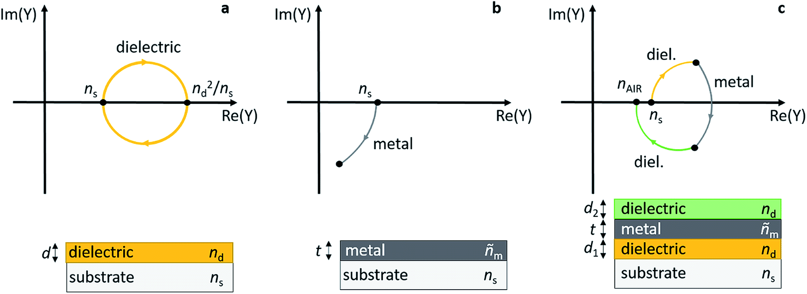 | ||
| Fig. 10 Admittance plots for a dielectric layer (a), a metal layer (b), and a dielectric/metal/dielectric sandwich (c) on top of a substrate. | ||
Obviously, the above concept can be applied for the design of transparent conductive electrodes. As a requirement, the dielectric must be replaced with a transparent (semi)conductor in order to interface the metal as an electrode to a thin film device. Thus, all kinds of transparent conductive oxides (TCOs) have been used to sandwich a thin metal electrode, i.e. TCO/metal/TCO. In contrast to the use of the TCOs as the electrode alone, the TCOs in the sandwich do not require to be highly conductive, as the metal provides a high lateral conductivity. Rather the optical properties of the TCO claddings should be tailored to fulfill the optical design criteria detailed above in the best possible way. Note that the admittance matching of course is subject to the dispersive optical properties of the layers involved. Typically, a high transmittance is achieved in some limited spectral region around the wavelength the optimization has been done for. In an attempt to broaden this window of high transmittance, Mouchaal et al. have proposed the use of a metal multilayer, e.g. Cu/Ag, in between the dielectric layers and achieved a high transmittance in a broad spectral range between 400 and 1000 nm.153
Our review will focus on fundamental concepts of TCO/metal/TCO electrodes and on the more recent results in the field. There are a few earlier review articles on TCO/metal/TCO electrodes for photovoltaic applications, which provide comprehensive tables of TCO/metal/TCO electrodes and their properties.154–156 Classically, among the most widely studied TCO/metal/TCO electrodes, ITO/metal/ITO is often abbreviated as IMI. As a metal layer, silver is typically used. The high conductivity of the metal relaxed the requirements for a high conductivity of the ITO, and thus allowed the ITO to be prepared at relatively low temperatures (<150 °C). Originally, IMI was studied as transparent conductive coating for thermally insulating windows, and requirements such as durability and thermal stability were of paramount interest.157–159 Bender and co-workers were the first to introduce IMI as a transparent electrode for flat-panel display applications.160 All layers in their electrode stack were deposited by DC-magnetron sputtering. For improved wetting, as discussed above, an alloy of 90% Ag and 10% Cu was used. In an optimized stack, a low sheet resistance of 5.7 Ω sq−1 and a maximum transmittance of 83% have been achieved, with a Haacke figure of merit twice as high as that of ITO alone. Aside from Ag, Au has also been used as an ultra-thin metal in the sandwich with ITO. An ITO 50 nm/Au 10 nm/ITO 40 nm electrode with a sheet resistance of 5.6 Ω sq−1 and an average optical transmittance of 72% in the visible region (400–700 nm) has been reported.161,162 Today, IMI can be prepared by roll-to-roll sputtering and it is commercialized as a transparent electrode on top of polymer foil substrates.163,164
For the reasons outlined in the introduction, an alternative transparent electrode should aim to avoid the use of ITO. In this sense, in 2003 Ito et al. used a TiO2/Ag/TiO2 sandwich as a front electrode in a dye sensitized solar cell.165 They achieved a sheet resistance of 8 Ω sq−1 and an average transmittance (400–700 nm) of 82%. In this particular application, however, the chemical reaction of the Ag and the iodine based electrolyte used in the solar cell promoted the formation of AgI which created notable reliability issues. In a one-by-one comparison of Nb2O5/Ag/Nb2O5 with the ITO based analogue almost identical transmittance and sheet resistance have been achieved.166 As Nb is about two orders of magnitude more abundant than In, this is a promising result. A very successful TCO for TCO/metal/TCO electrodes is ZnO. Highly conductive ZnO/Ag/ZnO electrodes with a sheet resistance as low as 3 Ω sq−1 and a concomitant high transmittance of 90% at 580 nm have been reported.167 ZnO can be easily doped by incorporating group-III elements, e.g. Al or Ga, and thereby the carrier density of the TCO increases by orders of magnitude without a substantial loss of transmittance in the visible spectral region.6 Instead, the doping pushes the Fermi-level into the conduction band of the TCO and the associated Burstein–Moss shift increased the onset of absorption to higher photon energies, thereby rendering the doped ZnO even more transparent in the short-wavelength range of the visible spectrum.168,169 This effect promised improved transparent electrodes. Al:ZnO/metal/Al:ZnO and Ga:ZnO/metal/Ga:ZnO have been demonstrated, but their figures of merit were not significantly better than those of ZnO/Ag/ZnO electrodes.170 Recently, Al:ZnO/Au/Al:ZnO electrodes have been reported on top of PET substrates, with the remarkable finding that the Au showed percolation already at 3 nm mass-equivalent in spite of the roughness of the Al:ZnO.171 The resulting electrodes were extremely flexible without loss of conductivity. Later the same group used an asymmetric TiO2/Au/Al:ZnO setup, and the figure of merit has been improved by a factor of three due to the lower roughness of the TiO2 layer.172
Further optimization has been achieved by increasing the bandgap of ZnO upon addition of Mg. Compared to ZnO/Ag/ZnO, the optical absorption edge of MgxZn1−xO/Ag/MgxZn1−xO is blue-shifted with increasing Mg content.173 Very recently, Lee et al. reported Mg0.28Zn0.72O/Ag (14 nm)/Mg0.28Zn0.72O with a sheet resistance of 6.36 Ω sq−1 and an average transmittance of 89.2% between 350 and 780 nm.174 The resulting Haacke figure of merit was 69% higher than that of a similar ZnO/Ag/ZnO multilayer electrode. This idea has been pushed even further by using ZnMgBeO/Ag/ZnMgBeO, where the ZnMgBeO had a bandgap of 4.5 eV. The resulting electrode has a transmittance of 74–90% in the UV-range of 300–400 nm.175
Unfortunately, many ZnO-based TCOs (neat and doped) have been associated with some limited chemical stability under damp heat conditions.176–180 It has been evidenced that in a moist ambient atmosphere the electrical conductivity of ZnO degrades due to the formation of –OH groups and chemisorbed oxygen.181 Tin-oxide (SnOx) and zinc-tin-oxide (ZTO) are known for their elevated chemical stability compared to ZnO.182–184 SnOx (25 nm)/Ag (5 nm)/SnOx (25 nm) prepared by magnetron sputtering provided a sheet resistance of 9.61 Ω sq−1 and a transmittance of 83% in the region of 400–800 nm.185 Bou et al. prepared SnOx/Ag/SnOx electrodes with a low Rsh = 6.7 Ω sq−1 at a somewhat lower average transmittance (between 400 and 700 nm) of 67%.186 Very recently, also SnOx/Au/SnOx multi-layers have been reported with Rsh = 52 Ω sq−1 and a transmittance of 83% for λ > 475 nm.187
Behrendt et al. used SnOx prepared by atomic layer deposition (ALD) to sandwich ultra-thin Ag or Cu layers (thickness 7 nm). A sheet resistance of 9 Ω sq−1 and 20 Ω sq−1 has been achieved for the Ag and Cu based sandwich electrodes, respectively (Fig. 11).180 In the case of the SnOx/Ag/SnOx electrode, an average transmittance of 82% (between 400 and 750 nm) has been found (Fig. 11c). As a special feature, the ALD prepared SnOx layers were shown to form extremely conformal and pin-hole-free gas permeation barriers with a water vapor transmission rate on the order of 10−6 g per m2 per day. This barrier property allowed for efficient encapsulation and protection of the sensitive thin metal layers. Unprotected Cu and Ag electrodes degraded within a few minutes when exposed to damp heat conditions (85 °C/85% rH), e.g. Cu films lose 7 orders of magnitude in electrical conductivity. In contrast, sandwich structures of SnOx/(Cu or Ag)/SnOx remained virtually unchanged even after more than 100 h (Fig. 11d). Chen et al. have reported corrosion of Ag layers in an IMI electrode at a slightly elevated temperature of 50 °C and high level of humidity of 90%.188 They demonstrated that an alloy of Ag–Ti instead of pure Ag was significantly more stable under the same conditions. A similar stabilizing effect has been found for Ag–Cr alloys in IMI electrodes.189
 | ||
| Fig. 11 Layer sequences of transparent conductive electrodes based on thin metal films sandwiched between SnOx transparent conductive gas diffusion barriers (a). Photographs of the resulting electrodes on glass substrates along with their electrical sheet resistance (b). Optical transmission/reflection/absorption data for the Ag based electrode in comparison to commercial ITO (c). The SnOx/Ag/SnOx electrode shown here has been designed for a minimum reflectivity between 550 and 650 nm. Normalized conductivity of transparent conductive electrodes based on thin Cu or Ag layers with and without protection under damp heat conditions (85 °C/85% rH) (d) (reproduced with permission. Wiley VCH (Weinheim) 2015).180 | ||
Fluorine doped SnO2 (FTO) has been used very recently to prepare a FTO (20 nm)/Ag (7 nm)/FTO (30 nm) electrode with a remarkable transmittance of 95.5% in the visible region and a sheet resistance of 8 Ω sq−1.190 Owing to the high transmittance of 95.5%, the resulting Haacke figure of merit sets these electrodes among the best TCO/metal/TCO electrodes, ever made. The claimed transmittance of 95.5% is even more remarkable, since the transmittance of a quartz glass substrate without an electrode is limited to roughly 95% due to reflection.
Choi et al. and Winkler et al. introduced ZTO/metal/ZTO electrodes.191–193 The ZTO was deposited by magnetron sputtering from a ZTO target at room temperature, and the resulting ZTO layers were found to be amorphous. Very recently, a higher critical strain for the onset of cracking was reported for ZTO films compared to AZO layers. This was attributed to the polycrystalline nature of AZO, where a high density of grain boundaries was claimed to function as crack initiators, in contrast to the amorphous ZTO without grain boundaries.194
A low sheet resistance of 8.8 Ω sq−1 and a transmittance of 82% in the visible region have been achieved with a stack of ZTO (20 nm)/Ag (8 nm)/ZTO (39 nm), resulting in a Haacke figure of merit about an order of magnitude better than that of ITO. In this comparison, the ITO layer (thickness: 60 nm) had been prepared under identical temperature conditions to those of the ZTO/Ag/ZTO, i.e. it had not been thermally annealed after deposition (Rsh = 83 Ω sq−1, T = 85%).192 Interestingly, the deposition of thin Ag layers on ZTO showed a lower percolation threshold compared to those deposited on molybdenum oxide (MoO3). Similar substrate effects on morphology and evolution of ultra-thin Au films have been observed by Lansåker et al.195 As shown in Fig. 12a, even a 6 nm thin Ag layer forms a continuous layer when sandwiched between ZTO claddings. Some Ag crystallites are clearly visible in HRTEM. Importantly, an initially percolated Ag layer on top of ZTO (ZA) has been found to de-wet and to form Ag-aggregates with a concomitant loss of conductivity when the sample was kept either in ambient air (Fig. 12b) or in an inert atmosphere. On the contrary, it has been verified that the de-wetting of the Ag was suppressed by the ZTO capping layer and the Ag layer was stabilized. Towards upscaling and commercialization, ZTO/Ag/ZTO electrodes with a sheet resistance of 8.38–10.18 Ω sq−1 and an average transmittance of 84.4–85.5% in the visible region have been prepared by inline sputtering using linear targets with a size of 10 × 40 cm2.196 Roll-to-roll sputter deposition of ZTO/Ag/ZTO electrodes onto poly(ethersulfone) (PES) and poly(ethylene terephthalate) (PET) has also been established.197,198 ZTO/Ag/ZTO electrodes have been used to prepare In-free large area OLEDs.199
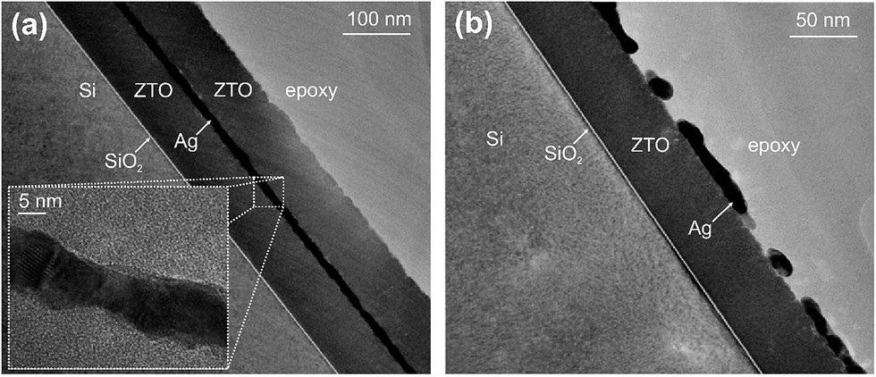 | ||
| Fig. 12 (a) Cross-sectional TEM image of the zinc-tin-oxide/Ag/zinc-tin-oxide (ZAZ) multilayer electrode. Inset: magnified view of the Ag layer in the sandwich. (b) Zinc-tin-oxide/Ag (ZA) structure deposited on a silicon substrate at room temperature, showing the agglomeration of an Ag layer after storage in ambient air for 500 h. Nominal thicknesses of the layers are 6 nm (Ag) and 60 nm (zinc-tin-oxide) (reproduced with permission. Copyright 2011, Elsevier).192 | ||
In most of the TCO/metal/TCO systems discussed so far, the TCOs have commonly been deposited by sputter deposition or electron/ion-beam assisted techniques. A major concern is the possible damage that the highly energetic particles may cause to sensitive substrates. This is problematic, if the transparent electrode must be applied on top of (organic) devices. High-energy sputter particles have been shown to damage the functional layers of organic electronic devices.200–202 A transparent electrode on top of a thin-film device is needed if an opaque substrate is used (e.g. for top-illuminated solar cells) or in case semi-transparent devices are envisaged, where transparent bottom and top-electrodes are needed. As a result, it is advantageous for the preparation of TCO/metal/TCO electrodes to use TCOs that can be deposited by thermal evaporation techniques. In this regard, transition metal oxides, like molybdenum oxide (MoO3), tungsten oxide (WO3), and vanadium oxide (V2O5), can be thermally evaporated from a Knudsen cell. As reported by Berkowitz and co-workers, MoO3 and WO3 sublime predominantly in the form of Mo3O9 or W3O9 trimers, which leads to the observation that thermally evaporated MoO3 and WO3 thin films are stoichiometric.203,204 Their optical and electrical properties have been reviewed by Meyer et al.205
The first report by Ryu et al. of a WO3 (40 nm)/Ag (12 nm)/WO3 (40 nm) semi-transparent electrode prepared by thermal evaporation at room temperature already afforded excellent characteristics with Rsh = 6 Ω sq−1 and a transmittance of 90% at 550 nm.206 The high conductivity of the WO3/Ag/WO3 (WAW) was on a par with that of the best ZnO/Ag/ZnO or ITO/Ag/ITO electrodes, in spite of the fact that the intrinsic conductivity of thermally deposited WO3 is typically orders of magnitude lower than that of TCOs like ZnO or ITO.205 As a further improvement, Hong et al. reported a transmittance of 93.5% and a Rsh = 6 Ω sq−1 for WO3 (30 nm)/Ag (12 nm)/WO3 (30 nm).207 WAW has been used to prepare high-performance, flexible ITO-free electrochromic devices.208 MoO3/Ag/MoO3 (MAM) electrodes with a similar performance to WAW have also been reported.209 Whereas MoO3 and WO3 have rather similar electronic and optical properties, the clear advantage of MAM over WAW is that MoO3 can be evaporated at substantially lower effusion cell temperatures compared to WO3.210,211 As will be seen below, MAM is one of the most widely used TCO/metal/TCO electrodes for thin-film solar cells. The electrical and optical properties of MAM electrodes have been modelled, and a good agreement of theory and experiment has been achieved.212 ZnS/Ag/ZnS multilayer electrodes can also be prepared entirely by thermal evaporation and they provided outstanding characteristics (Rsh = 3 Ω sq−1, T = 90%).213 It was argued that the aggregation of Ag layers on top of ZnS was suppressed and the percolated Ag layers showed improved thermal stability on ZnS compared to Ag on top of WO3 or MoO3. As a result, ZnS/Ag/MoO3 and ZnS/(Ag or Cu)/WO3 hybrid electrodes have been prepared.214,215 By a similar token, TeO2/Ag/MoO3 electrodes were found to be more transparent due to an earlier percolation of the Ag on top of the tellurium oxide compared to MoO3.216 It has to be noted, though, that Te belongs to the rarest elements in the earth crust and it is about an order of magnitude less abundant than indium.
WAW multilayer electrodes have also been realized with the WO3 prepared in a solution process. Tungstic acid has been used as a precursor, which after heat treatment (200 °C) transformed to a layer consisting of WO3 nanoparticles.217 The thin silver layer has been thermally evaporated. The resulting WAW electrodes had a remarkably high transmittance of 85% with a sheet resistance of 4 Ω sq−1.
An important added benefit of WAW and MAM electrodes is the high work-function of MoO3 and WO3, which labels these materials as hole-extraction layers which interface to a wide range of organic and perovskite photo-active materials.205
In an attempt to avoid Ag, MoO3/Cu/MoO3 and MoO3/Al/Cu/Al/MoO3 have been studied.218 In the latter case, 1 nm thin Al layers were inserted to prevent the otherwise significant diffusion of Cu into the oxide layers.
Very recently, organic/metal (Ag)/organic (OMO) semi-transparent electrodes have been reported, where the organic layers were polyvinylcarbazole (PVK) or PEDOT:PSS prepared from the liquid phase.219 The electrodes had a sheet resistance of less than 10 Ω sq−1 and a transmittance of 85%.219 Later gold-based PEDOT:PSS (35 nm)/Au (15 nm)/PEDOT:PSS (35 nm) electrodes have been reported.220 Aside from cost considerations, a commonly claimed advantage of these OMO electrodes is that their stability upon bending should be dramatically improved compared to their oxide based counterparts. An overview of the recent progress on semi-transparent electrodes based on thin metal layers is given in Table 2.
3.3. Applications of ultra-thin metal electrodes in thin-film solar cells
Similar to the case of AgNW electrodes, semi-transparent electrodes based on thin metal films are of great importance in organic opto-electronic devices, as a replacement for ITO and to overcome mechanical limits of ITO in flexible applications. Moreover, the relatively gentle thermal evaporation of metals like Ag, Au or Al affords their use as semi-transparent electrodes on top of the device stack. For organic solar cells (OSCs), top-illuminated devices on opaque substrates or semi-transparent cells can thus be realized. A wide range of earlier studies on organic solar cells incorporating dielectric/metal/dielectric electrodes has been reviewed by Guillén et al.154 and Cattin et al.155 Here, we intend to highlight the most recent work in the field of thin-film PV.In a comparative study, top-illuminated small-molecule OSCs with a top electrode based on AgNWs or a thin metal layer (Au/Ag) were investigated. A 1 nm thin Au layer served as a seed layer to improve the wetting of the Ag electrode.223 After encapsulation, the devices based on the thin metal electrodes were significantly more stable with T80 = 1000 h vs. T80 = 20 h for the AgNW based analogues. In the case of the NW electrode decomposition of the wires and a concomitant loss of conductivity were found.224
Very recently, Zhao and co-workers used a ZnO/Cu(N)/ZnO electrode on PET to prepare flexible OSCs with an efficiency of 7.1%, which was higher than that of the ITO based reference.147 In addition, the ZnO/Cu(N)/ZnO based devices allowed bending radii of less than 2 mm without loss of efficiency, while the ITO based devices were severely degraded due to an increased sheet resistance of the ITO upon bending. Zuo et al. suggested MoO3/Ag/MoO3 top electrodes for large area top-illuminated OSCs, where they deliberately introduced a lateral variation of the Ag thickness, thereby forming a conductance gradient over the active area. Specifically, as the top electrode served as the anode in their devices, they increased the Ag thickness towards the edge of the module where the (+)-lead was hooked up. Thereby they could control the light in-coupling over the active area and minimize resistive losses on large area (4 cm2) devices. This way, they managed to prepare large area devices which maintained 80% of the efficiency of their small-area analogues.225
An impressive 10.4% efficient top-illuminated flexible OSC has been realized by the use of a MoO3/Ag (12 nm)/TeO2 (40 nm) semi-transparent top-electrode.226 The design of the top-electrode allowed for efficient light in-coupling and its high lateral conductivity afforded 1 cm2 cells with a high efficiency of 7.21%. TeO2 was chosen because of its relatively high refractive index of n ≈ 2.2, which according to a transfer-matrix simulation allowed for the use of thicker Ag layers for optimum transmittance of the electrode.227 The same electrode concept has been applied in tandem OSCs, which gave a similar efficiency of about 7.5% for bottom-illuminated ITO-based reference devices (Fig. 13).228
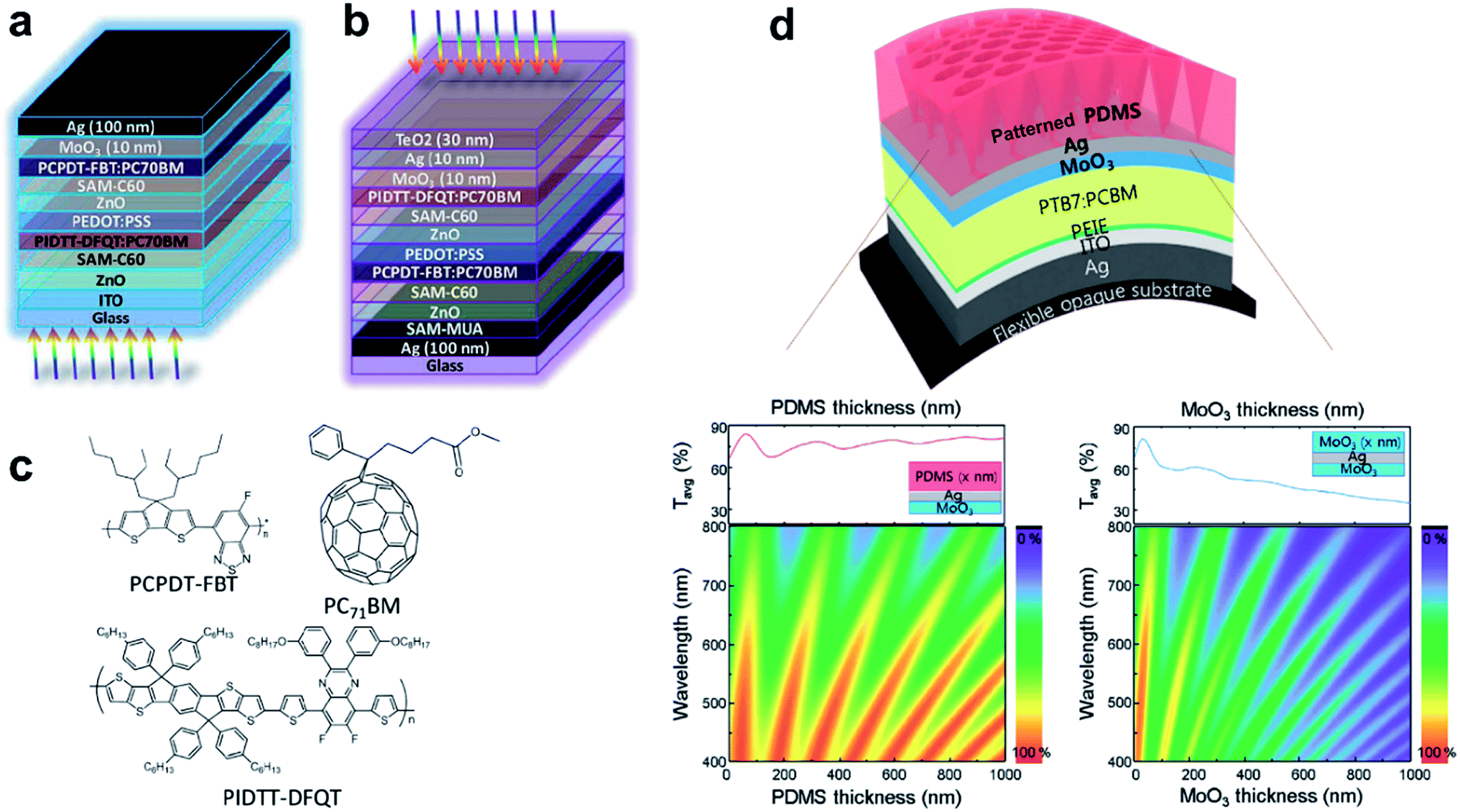 | ||
| Fig. 13 Schematic device configurations of the (a) ITO-based tandem solar cell and (b) top-illuminated tandem solar cell based on a MoO3/Ag/TeO2 top electrode. (c) Molecular structures of PCPDT–FBT, PIDTT–DFQT, and PC71BM (reproduced with permission, copyright 2016, The Royal Society of Chemistry).228 (d) Schematic illustration of the top illuminated organic solar cell using patterned MoO3/Ag/PDMS. Simulated 2D contour plots of the transmittance of MoO3/Ag/PDMS as a function of PDMS thickness and the transmittance of MoO3/Ag/MoO3 as a function of MoO3 thickness are plotted along with the average transmittance spectra (reproduced with permission, copyright 2016, Wiley VCH Weinheim).229 | ||
Ham et al. designed top-illuminated flexible organic solar cells with a MoO3/Ag/poly(dimethylsiloxan) (PDMS) semi-transparent top-electrode (Fig. 13d). As a specialty, the PDMS elastomer contained a nano-pattern which significantly increased the haze and improved light trapping. This afforded a 28% enhancement in efficiency compared to bottom illuminated cells.229 In general, there is a wide range of laterally patterned electrodes that have been used for enhanced light trapping in OSCs. The reader is kindly referred to a very recent review article on this particular topic by Chueh et al.230
In an attempt to control the color of semitransparent OSCs, top electrodes of WO3/Ag/1DPC were suggested, where 1DPC is a one-dimensional photonic crystal that consisted of [MoO3/LiF]#pairs or [WO3/LiF]#pairs.231,232 The 1DPC relied on the large refractive index contrast between MoO3 and LiF (2.11 and 1.44, respectively). The number of pairs (#pairs) in the 1DPC was varied between 1 and 5. In optimized devices, a color rendering index of 97 was achieved for cells with an efficiency of 5.31% and an average transmittance in the visible region of >25%.
 | ||
| Fig. 14 (a) Schematic illustration (not to scale) of the cell architecture. (b) SEM image of the cross-section of a complete device. (c) Enlarged view of the MoO3/Au/MoO3 multilayer top electrode and schematic of its structure. (d) Simulations (shaded dashed lines) and experimental data (solid lines) showing the transmittance of Au (black), bottom-MoO3/Au (red) and bottom-MoO3/Au/top-MoO3 (blue). (e) SEM image of the Au film. (f) SEM image of the bottom-MoO3/Au film. The insets show photos of the two samples (reproduced with permission, copyright 2015, Elsevier).233 | ||
Semi-transparent perovskite cells incorporating a micro-cavity that works as a color filter have been proposed by Lee et al. The micro-cavity was constructed by sandwiching a WO3 layer of variable thickness between two thin Ag layers (20 nm). This assembly served both as the cathode of the perovskite cells and as the color-filter. The resulting devices showed a variation of distinctive transmitted colors ranging from red to blue.235 An identical approach using ITO instead of WO3 between two thin Ag layers was reported by Lu et al.236
Very recently, Kim et al. introduced semitransparent perovskite cells with a MoO3/Ag/ZnS sandwich that served as a transparent top electrode and reflector for near-infrared (NIR) radiation, at the same time (Fig. 15).237 Their cells showed an average power conversion efficiency as large as 13.3%, an average transmittance of 7.42% in the visible region, and a NIR reflectance of 85.5%, which is of interest for window-integrated PV. The balance between transmittance in the visible and reflectance in the NIR is visualized by an admittance plot (Fig. 15c).
 | ||
| Fig. 15 (a) Layer sequence of the semi-transparent perovskite solar cell. (b) Schematic configuration of the MoOx (7 nm)/Ag (dAg)/ZnS (dcap) (=MAZ) layers on top of spiro-MeOTAD. (c) Admittance diagram for an MAZ stack (dAg = 12 nm; dcap = 30 nm) drawn by starting at the admittance of air followed by stacking each layer up to the indicated thickness at two different wavelengths of 550 nm (black, solid) and 1500 nm (green, dashed). The red dot indicates the admittance of the spiro-MeOTAD medium. (d) A graph showing the maximum achievable transmittance (Tmax at λ = 550 nm) of MoOx (7 nm)/Ag (dAg = 12, 18, or 24 nm)/capping layer (dcap) as a function of the refractive index (n) of its capping layer. dcap is optimized for maximal transmittance at λ = 550 nm. In (c) and (d), spiro-MeOTAD, from which light is incident, is assumed to fill the half-infinite space for this calculation (reproduced with permission, copyright 2016, Wiley VCH Weinheim).237 | ||
Zhou et al. demonstrated a semitransparent perovskite solar cell with MoO3/Au/MoO3 as a transparent electrode that has been vertically integrated with an electrochromic supercapacitor.238 The color states of the devices indicated the amount of energy stored and the amount of energy consumed in real time. Moreover, the photo-stability of the device was improved by shutting off the long-time photo-exposure if the capacitor was fully charged.
Lee et al. showed colored a-Si thin film PV based on a metal–semiconductor–metal resonator like assembly.241 The semi-transparent bottom-electrode was WO3/PTCBI/Ag/V2O5 (Fig. 16). Here, perylene-tetracarboxylic bis-benzimidazole (PTCBI) was used as a seed layer which caused less absorption than other seed materials, e.g. Ge. V2O5 with its high work-function242 served as a hole-extraction layer. The color variation is achieved by a variation of the a-Si thickness between 10 and 27 nm. The resulting colored devices had an efficiency of about 3% and were claimed to be promising for decorative PV applications in architecture.
 | ||
| Fig. 16 (a) The device structure for colored a-Si based cells. A WO3/PTCBI/Ag/V2O5 stack is used as the anode. Between the two electrodes is an ultrathin a-Si layer. (b) The band diagram of an a-Si photoactive layer interfaced with ICBA and V2O5. (c) The University of Michigan logo, consisting of green and blue colors, is successfully realized. (d) Current density vs. voltage (J–V) characteristics of the maize-and-blue-colored, 1 mm-diameter devices under AM1.5 illumination. AM, air mass; a-Si, amorphous silicon; ICBA, indene-C60 bis-adduct (reproduced with permission, copyright 2014, Nature Publishing Group).241 | ||
| Electrode structure thickness of the layers | Deposition technique | Electrical and optical properties (optimum) | Chemical and thermal stability | Mechanical properties | Ref. and year |
|---|---|---|---|---|---|
| ITO/AgCu/ITO, 50 nm/10 nm/50 nm | DC magnetron sputtering of all layers, an Ag(90%)Cu(10%) alloy target was used | T max = 83% | No data | No data | 160 and 1998 |
| R sh = 5.7 Ω sq−1 | |||||
| FOM = 0.027 Ω−1 | |||||
| ITO/Au/ITO, 50 nm/10 nm/40 nm | Reactive RF magnetron sputtering for the ITO layers, DC sputtering for the Au; substrate temperature 70 °C | T av = 72% | No data | No data | 161 and 162, 2010 |
| R sh = 5.6 Ω sq−1 | |||||
| FOM = 0.007 Ω−1 | |||||
| TiO2/Ag/TiO2, 20 nm/10 nm/30 nm | Reactive DC sputtering | T av = 82% | Ag reacted with the iodine used in dye sensitized solar cells | No data | 165 and 2003 |
| R sh = 8 Ω sq−1 | |||||
| FOM = 0.017 Ω−1 | |||||
| Nb2O5/Ag/Nb2O5 | Multi-chamber roll-to-roll sputtering; DC sputtering for Ag and 45 kHz AC sputtering for Nb2O5 | T 550 nm = 83% | No data | No data | 166 and 2006 |
| R sh = 7.1 Ω sq−1 | |||||
| FOM = 0.022 Ω−1 | |||||
| ZnO/Ag/ZnO, 20 nm/6 nm/20 nm | In-line RF/DC sputtering | T 580 nm = 90% | No data | No data | 167 and 2006 |
| R sh = 3 Ω sq−1 | |||||
| FOM = 0.12 Ω−1 | |||||
| ZnO/Cu(N)/ZnO, 60 nm/6.5 nm/60 nm | RF magnetron sputtering; for the Cu gas mixture Ar + N2 | T 380–1000 nm = 84% | Stable at 85 °C/85% rH for 800 h | No degradation upon bending (radius < 2 mm) | 147 and 2016 |
| R sh = 20 Ω sq−1 | |||||
| FOM = 0.009 Ω−1 | |||||
| AZO/Ag/AZO, 40 nm/12 nm/40 nm | Tilted dual target DC magnetron sputtering; GZO target (3 wt% Ga2O3-doped ZnO); AZO target (5 wt% Al2O3-doped ZnO) | T 550 nm (AZO) = 82% | No data | No data | 170 and 2009 |
| R sh (AZO) = 6 Ω sq−1 | |||||
| FOM (AZO) = 0.023 Ω−1 | |||||
| GZO/Ag/GZO 40 nm/12 nm/40 nm | T 550 nm (GZO) = 87% | ||||
| R sh (GZO) = 6 Ω sq−1 | |||||
| FOM (GZO) = 0.04 Ω−1 | |||||
| AZO/Au/AZO, 50 nm/11 nm/50 nm | DC magnetron sputtering; AZO target (2 wt% Al2O3-doped ZnO) | T 550 nm = 75% | No data | R sh increased by 20% after 400 bending cycles (radius: 4.5 mm) | 171 and 2015 |
| R sh = 7 Ω sq−1 | |||||
| FOM = 0.008 Ω−1 | |||||
| TiOx/Au/AZO, 36 nm/9 nm/63 nm | DC magnetron sputtering, metal Ti target for deposition of TiOx in Ar/O2 atmosphere, AZO target (2 wt% Al2O3-doped ZnO) | T 550 nm = 88% | No data | No data | 172 and 2016 |
| R sh = 14 Ω sq−1 | |||||
| FOM = 0.02 Ω−1 | |||||
| MgZnO/Ag/MgZnO, 50 nm/14 nm/50 nm | Mg:ZnO by RF magnetron sputtering using dual targets, ZnO and ZnO:20%MgO, Ag layer by electron beam deposition | T av = 89.2% | No data | No data | 174 and 2016 |
| R sh = 6.4 Ω sq−1 | |||||
| FoM = 0.05 Ω−1 | |||||
| SnOx/Ag/SnOx, 25 nm/5 nm/25 nm | SnO2 by RF magnetron sputtering in Ar/O2 atmosphere; Ag by DC magnetron sputtering in Ar atmosphere | T 550 nm = 83% | No data | No data | 185 and 2012 |
| R sh = 9.6 Ω sq−1 | |||||
| FOM = 0.016 Ω−1 | |||||
| SnOx/Ag/SnOx, 47 nm/10 nm/45 nm | Electron beam evaporation in vacuum | T av = 67% | No data | No data | 186 and 2014 |
| R sh = 6.7 Ω sq−1 | |||||
| FOM = 0.003 Ω−1 | |||||
| SnOx/Au/SnOx, 35 nm/5.2 nm/35 nm | Electron beam evaporation of SnOx and thermal evaporation of Au | T >475 nm = 83% | No data | No data | 187 and 2016 |
| R sh = 52 Ω sq−1 | |||||
| FOM = 0.003 Ω−1 | |||||
| SnOx/Ag/SnOx, SnOx/Cu/SnOx, 75 nm/7 nm/50 nm | SnOx prepared by atomic layer deposition (ALD), Ag and Cu were RF magnetron sputtered | T av (Ag) = 82% | ALD-SnOx layers are gas diffusion barriers against water and oxygen; electrodes stable at 85 °C/85% rH >100 h | No change in Rsh upon bending (radius: 20 mm) | 180 and 2015 |
| R sh (Ag) = 9 Ω sq−1 | |||||
| FOM (Ag) = 0.015 Ω−1 | |||||
| F:SnO2/Ag/F:SnO2, 20 nm/7 nm/30 nm | RF magnetron sputtering of F:SnO2 using a mixed SnO2/SnF2 (20 at% of F) target, Ag by DC sputtering | T vis = 95.5% | No data | No data | 190 and 2016 |
| R sh = 8 Ω sq−1 | |||||
| FOM = 0.078 Ω−1 | |||||
| ZTO/Ag/ZTO, 35 nm/12 nm/35 nm | RF magnetron sputtering for ZTO (target: 35 wt%, ZnO-65 wt% SnO2); DC magnetron sputtering for Ag | T max = 86.3% | No data | No data | 191 and 2011 |
| R sh = 4 Ω sq−1 | |||||
| FOM = 0.057 Ω−1 | |||||
| ZTO/Ag/ZTO, 20 nm/8 nm/40 nm | RF magnetron sputtering for ZTO (target: SnO2/ZnO (50:50 at%)); Ag by thermal evaporation in vacuum |
T vis = 82% | No data | No data | 192 and 193, 2011 |
| R sh = 8.8 Ω sq−1 | |||||
| FOM = 0.02 Ω−1 | |||||
| ZTO/Ag/ZTO, 40 nm/10 nm/40 nm | RF magnetron and DC pulsed inline sputtering for ZTO and Ag, respectively; target size 10 × 40 cm2; ZnO/SnO2 target (30:70 wt%) |
T vis = 84.4–85.5% | No data | No data | 196 and 2014 |
| R sh = 8.38–10.18 Ω sq−1 | |||||
| FOM = 0.025 Ω−1 | |||||
| ZTO/Ag/ZTO, 40 nm/12 nm/40 nm | Roll-2-roll RF sputtering; ZTO target 35 wt% ZnO–65 wt%, SnO2 | T = 86.3% | No data | Stable upon 50000 bending cycles (radius: 10 mm), cracks start at 3% uniaxial strain |
197 and 2011 |
| R sh = 5.1 Ω sq−1 | 198 and 2012 | ||||
| FOM = 0.042 Ω−1 | |||||
| WO3/Ag/WO3, 40 nm/12 nm/40 nm | All layers were prepared by thermal evaporation | T 550 nm = 90% | No data | No data | 206 and 2008 |
| R sh = 6 Ω sq−1 | |||||
| FOM = 0.058 Ω−1 | |||||
| WO3/Ag/WO3, 30 nm/12 nm/30 nm | All layers were prepared by thermal evaporation | T 500 nm = 93.5% | No data | No data | 207 and 2011 |
| R sh = 6 Ω sq−1 | |||||
| FOM = 0.085 Ω−1 | |||||
| WO3/Ag/WO3, 30 nm/10 nm/40 nm | All layers were prepared by electron beam evaporation | T vis > 80% | No data | No data | 208 and 2015 |
| R sh = 12.2 Ω sq−1 | |||||
| FOM = 0.009 Ω−1 | |||||
| WO3/Ag/WO3, 45 nm/15 nm/45 nm | WO3 processed from a tungstic-acid/isopropyl-alcohol precursor solution, baked at 200 °C, Ag thermally evaporated | T vis = 85% | No data | No data | 217 and 2012 |
| R sh = 4 Ω sq−1 | |||||
| FOM = 0.049 Ω−1 | |||||
| MoO3/Ag/MoO3, 20 nm/10 nm/35 nm | All layers were prepared by thermal evaporation | T av = 70% | No data | No data | 212 and 2012 |
| R sh = 1.4 Ω sq−1 | |||||
| FOM = 0.02 Ω−1 | |||||
| MoO3/Ag/MoO3, 5 nm/13 nm/40 nm | All layers were prepared by thermal evaporation | T 550 nm = 80% | No data | No data | 221 and 2012 |
| R sh = 5 Ω sq−1 | |||||
| FOM = 0.02 Ω−1 | |||||
| MoO3/Au/MoO3, 5 nm/10 nm/35 nm | All layers were prepared by thermal evaporation | T 650 nm = 90% | No data | No data | 233 and 2015 |
| R sh = 13–15 Ω sq−1 | |||||
| FOM = 0.027 Ω−1 | |||||
| MoO3/Au/Ag/MoO3, 10 nm/1 nm/10 nm/40 nm | All layers were prepared by thermal evaporation | T 550 nm = 80% | No data | No data | 234 and 2015 |
| R sh = 16 Ω sq−1 | |||||
| FOM = 0.007 Ω−1 | |||||
| MoO3/Al/Cu/Al/MoO3, 20 nm/1.4 nm/18 nm/1.4/35 nm | All layers were prepared by thermal evaporation | T 580 nm = 70% | No data | No data | 218 and 2012 |
| R sh = 66 Ω sq−1 | |||||
| FOM = 0.00043 Ω−1 | |||||
| TeO2/Ag/MoO3, 10 nm/8 nm/10 nm | All layers were prepared by thermal evaporation | T av = 77.1% | No data | No data | 216 and 2016 |
| R sh = 5 Ω sq−1 | |||||
| FOM = 0.02 Ω−1 | |||||
| MoO3/Ag/ZnS, 7 nm/12 nm/30 nm | All layers were prepared by thermal evaporation | T 550 nm = 85% | No data | No data | 237 and 2016 |
| R sh = 8.5 Ω sq−1 | |||||
| FOM = 0.023 Ω−1 | |||||
| MoOx/Ag/ZnS, 7 nm/17 nm/24 nm | All layers were prepared by thermal evaporation | T 550 nm = 80% | No data | No data | 222 and 2014 |
| R sh = 3.6 Ω sq−1 | |||||
| FOM = 0.02 Ω−1 | |||||
| ZnS/Ag/ZnS, 40 nm/18 nm/40 nm | All layers were prepared by thermal evaporation | T 550 nm = 86% | FOM stable at T < 200 °C, at higher temperatures degradation of Rsh due to chemical reaction and of T due to Ag diffusion | No data | 213 and 2001 |
| R sh = 3 Ω sq−1 | |||||
| FOM = 0.073 Ω−1 | |||||
| ZnS/Ag/MoO3, 27 nm/7 nm/5 nm | All layers were prepared by thermal evaporation | T 550 nm = 83% | No data | No change fo Rsh after 1000 bending cycles (radius: 2 mm) | 214 and 215, 2013 |
| R sh = 9.6 Ω sq−1 | |||||
| FOM = 0.073 Ω−1 | |||||
| PVK/Ag/PVK, 35–55 nm/12 nm/>10 nm | Ag by thermal evaporation, PVK poly(N-vinylcarbazole) and PEDOT from solution | T max = 85% | No data | In organic solar cells 75% of the initial PCE was maintained after 2000 bending cycles | 219 and 2015 |
| PVK/Ag/PEDOT:PSS, 40β-60 nm/12 nm/>15 nm | T av = 69% | ||||
| R sh = 10 Ω sq−1 | |||||
| FOMmax = 0.019 Ω−1 | |||||
| FOMav = 0.0024 Ω−1 | |||||
| PEDOT:PSS/Au/PEDOT:PSS, 35 nm/15 nm/35 nm | PEDOT:PSS solution processed, DC sputtering of Au | T vis = 82.9% | No data | Increase of Rsh by 3.8% after 2000 bending cycles (radius: 6 mm) | 220 and 2016 |
| R sh = 20.6 Ω sq−1 | |||||
| FOM = 0.0074 Ω−1 |
4. Concluding remarks
To conclude, our review of semi-transparent electrodes based on metal nanowires (1D) or ultra-thin metal layers (2D) is intended to provide the reader with a comparative overview over the basic concepts underlying these electrodes along with some general considerations for their design and preparation. We outlined the impressive recent progress in the field. Today, metal-based transparent electrodes can be realized at a large area, at low costs and low temperature. They are mechanically flexible and afford a conductivity and transmittance even better than those of established transparent conductors. A further focus of our article was to highlight the most recent applications of these semi-transparent electrodes in thin-film photovoltaic devices. In the field of nano-wire based electrodes, AgNWs owing to their availability are by far the dominating platform. Their demonstrated low sheet resistance sets these electrodes at par with ITO. The optical properties of NW-based electrodes are affected by the plasmonic properties of the metal and the resulting scattering/haze of the electrode may be beneficial for improved light trapping in solar cells. For enhanced mechanical, thermal and chemical stability, the NWs are frequently embedded into a conductive matrix of a metal oxide or an organic conductive medium to form hybrid electrodes, which have been used to replace ITO in a wide range of thin-film solar cells. In organo-metal halide perovskite solar cells, particular care has to be taken in order to avoid the detrimental chemical attack of the Ag due to corrosive halide based perovskite precursors or their decomposition compounds. Alternative materials like CuNW or AuNW have entered the scene but their availability is still limited and their application in devices is in its infancy. Metal NW based semi-transparent electrodes are naturally complemented by concepts based on ultra-thin metal layers with a thickness near/slightly above the percolation threshold. Despite the notable history of thin metal layers as semi-transparent electrodes, the field is full of vibrant activity, and we believe to have shown a number of impressive improvements that have been achieved in the past couple of years. We have shown that hybrid concepts such as sandwich structures of thin metal layers with less conductive metal-oxides or polymers unlock the region of extremely high figures of merit for transparent conductors. We have highlighted some selected applications of these semi-transparent electrodes in (semi-transparent) thin-film photovoltaic devices. Notably, these semi-transparent electrodes enable novel functionalities that encompass colored, semi-transparent and potentially heat reflecting solar modules, which may strengthen the unique selling points of thin-film photovoltaics.Acknowledgements
We acknowledge the German Federal Ministry for Education and Research (Grant No. 03EK3529E) and the Deutsche Forschungsgemeinschaft (DFG) (Grant: RI1551/4-2) for financial support.References
- W. F. Wu and B. S. Chiou, Appl. Surf. Sci., 1993, 68, 497–504 Search PubMed
.
- T. S. Sathiaraj, Microelectron. J., 2008, 39, 1444–1451 Search PubMed
- K. Sreenivas, T. S. Rao, A. Mansingh and S. Chandra, J. Appl. Phys., 1985, 57, 384–392 Search PubMed
- H. Kim, J. S. Horwitz, G. P. Kushto, Z. H. Kafafi and D. B. Chrisey, Appl. Phys. Lett., 2001, 79, 284–286 Search PubMed
- K. N. Rao, Indian J. Pure Appl. Phys., 2004, 42, 201–204 CAS
- T. Minami, Semicond. Sci. Technol., 2005, 20, S35–S44 CrossRef CAS
- V. Bilgin, I. Akyuz, E. Ketenci, S. Kose and F. Atay, Appl. Surf. Sci., 2010, 256, 6586–6591 CrossRef CAS
- N. Noor and I. P. Parkin, J. Mater. Chem. C, 2013, 1, 984–996 RSC
- P. S. Shewale, S. I. Patil and M. D. Uplane, Semicond. Sci. Technol., 2010, 25, 115008 CrossRef
- S. Rahmane, M. A. Djouadi, M. S. Aida, N. Barreau, B. Abdallah and N. H. Zoubir, Thin Solid Films, 2010, 519, 5–10 CrossRef CAS
-
D. Ginley, H. Hosono and D. C. Paine, Handbook of Transparent Conductors, Springer, US, 2010 Search PubMed
- A. Stadler, Materials, 2012, 5, 661–683 CrossRef
- R. M. Pasquarelli, D. S. Ginley and R. O'Hayre, Chem. Soc. Rev., 2011, 40, 5406–5441 RSC
- D. M. Sun, C. Liu, W. C. Ren and H. M. Cheng, Small, 2013, 9, 1188–1205 CrossRef CAS PubMed
- S. Park, M. Vosguerichian and Z. A. Bao, Nanoscale, 2013, 5, 1727–1752 RSC
- J. H. Du, S. F. Pei, L. P. Ma and H. M. Cheng, Adv. Mater., 2014, 26, 1958–1991 CrossRef CAS PubMed
- I. Jeon, K. Cui, T. Chiba, A. Anisimov, A. G. Nasibulin, E. I. Kauppinen, S. Maruyama and Y. Matsuo, J. Am. Chem. Soc., 2015, 137, 7982–7985 CrossRef CAS PubMed
- Y.-H. Hwang, M. Han, J. Lim, G. S. Lee and D. Jung, Fullerenes, Nanotubes, Carbon Nanostruct., 2016, 24, 305–312 CrossRef CAS
- E. Kymakis, K. Savva, M. M. Stylianakis, C. Fotakis and E. Stratakis, Adv. Funct. Mater., 2013, 23, 2742–2749 CrossRef CAS
- X. Xu, D. Huang, K. Cao, M. Wang, S. M. Zakeeruddin and M. Grätzel, Sci. Rep., 2013, 3, 1489 Search PubMed
- J.-Y. Lee, S. T. Connor, Y. Cui and P. Peumans, Nano Lett., 2008, 8, 689–692 CrossRef CAS PubMed
- S. R. Ye, A. R. Rathmell, Z. F. Chen, I. E. Stewart and B. J. Wiley, Adv. Mater., 2014, 26, 6670–6687 CrossRef CAS PubMed
- D. Langley, G. Giusti, C. Mayousse, C. Celle, D. Bellet and J.-P. Simonato, Nanotechnology, 2013, 24, 452001 CrossRef PubMed
- V. B. Nam and D. Lee, Nanomaterials, 2016, 6, 47 CrossRef
- C. Gu, N. Huang, J. Gao, F. Xu, Y. Xu and D. Jiang, Angew. Chem., Int. Ed., 2014, 53, 4850–4855 CrossRef CAS PubMed
- F. Selzer, C. Floresca, D. Kneppe, L. Bormann, C. Sachse, N. Weiss, A. Eychmuller, A. Amassian, L. Muller-Meskamp and K. Leo, Appl. Phys. Lett., 2016, 108, 163302 CrossRef
- A. T. Bellew, H. G. Manning, C. G. da Rocha, M. S. Ferreira and J. J. Boland, ACS Nano, 2015, 9, 11422–11429 CrossRef CAS PubMed
- E. C. Garnett, W. S. Cai, J. J. Cha, F. Mahmood, S. T. Connor, M. G. Christoforo, Y. Cui, M. D. McGehee and M. L. Brongersma, Nat. Mater., 2012, 11, 241–249 CrossRef CAS PubMed
- C. H. Liu and X. Yu, Nanoscale Res. Lett., 2011, 6, 75 CrossRef PubMed
- L. B. Hu, H. S. Kim, J. Y. Lee, P. Peumans and Y. Cui, ACS Nano, 2010, 4, 2955–2963 CrossRef CAS PubMed
- D. Y. Choi, H. W. Kang, H. J. Sung and S. S. Kim, Nanoscale, 2013, 5, 977–983 RSC
- D. Langley, G. Giusti, C. Mayousse, C. Celle, D. Bellet and J. P. Simonato, Nanotechnology, 2013, 24, 452001 CrossRef PubMed
- M. Lagrange, D. P. Langley, G. Giusti, C. Jimenez, Y. Brechet and D. Bellet, Nanoscale, 2015, 7, 17410–17423 RSC
- K. Zilberberg, F. Gasse, R. Pagui, A. Polywka, A. Behrendt, S. Trost, R. Heiderhoff, P. Gorrn and T. Riedl, Adv. Funct. Mater., 2014, 24, 1671–1678 CrossRef CAS
- R. M. Mutiso, M. C. Sherrott, A. R. Rathmell, B. J. Wiley and K. I. Winey, ACS Nano, 2013, 7, 7654–7663 CrossRef CAS PubMed
- D. Pu, W. Zhou, Y. Li, J. Chen, J. Chen, H. Zhang, B. Mi, L. Wang and Y. Ma, RSC Adv., 2015, 5, 100725–100729 RSC
- S.-k. Duan, Q.-l. Niu, J.-f. Wei, J.-b. He, Y.-a. Yin and Y. Zhang, Phys. Chem. Chem. Phys., 2015, 17, 8106–8112 RSC
- J.-W. Liu, J.-L. Wang, Z.-H. Wang, W.-R. Huang and S.-H. Yu, Angew. Chem., Int. Ed., 2014, 53, 13477–13482 CrossRef CAS PubMed
- T. Gao, B. Wang, B. Ding, J.-k. Lee and P. W. Leu, Nano Lett., 2014, 14, 2105–2110 CrossRef CAS PubMed
- D. Paeng, J.-H. Yoo, J. Yeo, D. Lee, E. Kim, S. H. Ko and C. P. Grigoropoulos, Adv. Mater., 2015, 27, 2762–2767 CrossRef CAS PubMed
- Q. Nian, M. Saei, Y. Xu, G. Sabyasachi, B. Deng, Y. P. Chen and G. J. Cheng, ACS Nano, 2015, 9, 10018–10031 CrossRef CAS PubMed
- H. F. Lu, D. Zhang, X. G. Ren, J. Liu and W. C. H. Choy, ACS Nano, 2014, 8, 10980–10987 CrossRef CAS PubMed
- Q. Xie, C. Yang, Z. Zhang and R. Zhang, High performance silver nanowire based transparent electrodes reinforced by conductive polymer adhesive, 16th International Conference on Electronic Packaging Technology (ICEPT), 2015, 1129–1133.
- C. H. Chung, T. B. Song, B. Bob, R. Zhu and Y. Yang, Nano Res., 2012, 5, 805–814 CrossRef CAS
- J. L. Elechiguerra, L. Larios-Lopez, C. Liu, D. Garcia-Gutierrez, A. Camacho-Bragado and M. J. Yacaman, Chem. Mater., 2005, 17, 6042–6052 CrossRef CAS
- J. T. Jiu, J. Wang, T. Sugahara, S. Nagao, M. Nogi, H. Koga, K. Suganuma, M. Hara, E. Nakazawa and H. Uchida, RSC Adv., 2015, 5, 27657–27664 RSC
- S. K. Hau, H. L. Yip, J. Y. Zou and A. K. Y. Jen, Org. Electron., 2009, 10, 1401–1407 CrossRef CAS
- M. Jorgensen, K. Norrman and F. C. Krebs, Sol. Energy Mater. Sol. Cells, 2008, 92, 686–714 CrossRef
- L. S. C. Pingree, B. A. MacLeod and D. S. Ginger, J. Phys. Chem. C, 2008, 112, 7922–7927 CAS
- F. So and D. Kondakov, Adv. Mater., 2010, 22, 3762–3777 CrossRef CAS PubMed
- C. Mayousse, C. Celle, A. Fraczkiewicz and J. P. Simonato, Nanoscale, 2015, 7, 2107–2115 RSC
- T. Leijtens, G. E. Eperon, N. K. Noel, S. N. Habisreutinger, A. Petrozza and H. J. Snaith, Adv. Energy Mater., 2015, 5, 1500963 CrossRef
- A. Kim, Y. Won, K. Woo, C. H. Kim and J. Moon, ACS Nano, 2013, 7, 1081–1091 CrossRef CAS PubMed
- Q. Huang, W. Shen, X. Fang, G. Chen, Y. Yang, J. Huang, R. Tan and W. Song, ACS Appl. Mater. Interfaces, 2015, 7, 4299–4305 CAS
- T. B. Song, Y. S. Rim, F. M. Liu, B. Bob, S. L. Ye, Y. T. Hsieh and Y. Yang, ACS Appl. Mater. Interfaces, 2015, 7, 24601–24607 CAS
- T. L. Chen, D. S. Ghosh, V. Mkhitaryan and V. Pruneri, ACS Appl. Mater. Interfaces, 2013, 5, 11756–11761 CAS
- B. Deng, P. C. Hsu, G. C. Chen, B. N. Chandrashekar, L. Liao, Z. Ayitimuda, J. X. Wu, Y. F. Guo, L. Lin, Y. Zhou, M. Aisijiang, Q. Xie, Y. Cui, Z. F. Liu and H. L. Peng, Nano Lett., 2015, 15, 4206–4213 CrossRef CAS PubMed
-
S. K. S. Jewell, Mineral Commodity Summaries, U.S. Geological Survey, 2011 Search PubMed
- A. R. Rathmell, S. M. Bergin, Y.-L. Hua, Z.-Y. Li and B. J. Wiley, Adv. Mater., 2010, 22, 3558–3563 CrossRef CAS PubMed
- A. R. Rathmell and B. J. Wiley, Adv. Mater., 2011, 23, 4798–4803 CrossRef CAS PubMed
- D. Zhang, R. Wang, M. Wen, D. Weng, X. Cui, J. Sun, H. Li and Y. Lu, J. Am. Chem. Soc., 2012, 134, 14283–14286 CrossRef CAS PubMed
- Y. Cheng, S. L. Wang, R. R. Wang, J. Sun and L. Gao, J. Mater. Chem. C, 2014, 2, 5309–5316 RSC
- W. L. Hu, R. R. Wang, Y. F. Lu and Q. B. Pei, J. Mater. Chem. C, 2014, 2, 1298–1305 RSC
- S. Ye, I. E. Stewart, Z. Chen, B. Li, A. R. Rathmell and B. J. Wiley, Acc. Chem. Res., 2016, 49, 442–451 CrossRef CAS PubMed
- Z. Chen, S. Ye, I. E. Stewart and B. J. Wiley, ACS Nano, 2014, 8, 9673–9679 CrossRef CAS PubMed
- P.-C. Hsu, H. Wu, T. J. Carney, M. T. McDowell, Y. Yang, E. C. Garnett, M. Li, L. Hu and Y. Cui, ACS Nano, 2012, 6, 5150–5156 CrossRef CAS PubMed
- A. R. Rathmell, M. Nguyen, M. Chi and B. J. Wiley, Nano Lett., 2012, 12, 3193–3199 CrossRef CAS PubMed
- Y. Won, A. Kim, D. Lee, W. Yang, K. Woo, S. Jeong and J. Moon, NPG Asia Mater., 2014, 6, e132 CrossRef CAS
- I. E. Stewart, A. R. Rathmell, L. Yan, S. R. Ye, P. F. Flowers, W. You and B. J. Wiley, Nanoscale, 2014, 6, 5980–5988 RSC
- J. Chen, J. Chen, Y. Li, W. Zhou, X. Feng, Q. Huang, J.-G. Zheng, R. Liu, Y. Ma and W. Huang, Nanoscale, 2015, 7, 16874–16879 RSC
- S. Ding, J. T. Jiu, Y. H. Tian, T. Sugahara, S. Nagao and K. Suganuma, Phys. Chem. Chem. Phys., 2015, 17, 31110–31116 RSC
- Z. Zhong, K. Woo, I. Kim, H. Hwang, S. Kwon, Y.-M. Choi, Y. Lee, T.-M. Lee, K. Kim and J. Moon, Nanoscale, 2016, 8, 8995–9003 RSC
- W.-K. Kim, S. Lee, D. Hee Lee, I. Hee Park, J. Seong Bae, T. Woo Lee, J.-Y. Kim, J. Hun Park, Y. Chan Cho, C. Ryong Cho and S.-Y. Jeong, Sci. Rep., 2015, 5, 10715 CrossRef CAS PubMed
- R. Adelung, O. C. Aktas, J. Franc, A. Biswas, R. Kunz, M. Elbahri, J. Kanzow, U. Schurmann and F. Faupel, Nat. Mater., 2004, 3, 375–379 CrossRef CAS PubMed
- K. D. M. Rao, R. Gupta and G. U. Kulkarni, Adv. Mater. Interfaces, 2014, 1, 1400090 CrossRef
- C. Hunger, K. D. M. Rao, R. Gupta, C. R. Singh, G. U. Kulkarni and M. Thelakkat, Energy Technol., 2015, 3, 638–645 CrossRef CAS
- K. D. M. Rao, C. Hunger, R. Gupta, G. U. Kulkarni and M. Thelakkat, Phys. Chem. Chem. Phys., 2014, 16, 15107–15110 RSC
- W. Zhou, J. Chen, Y. Li, D. Wang, J. Chen, X. Feng, Z. Huang, R. Liu, X. Lin, H. Zhang, B. Mi and Y. Ma, ACS Appl. Mater. Interfaces, 2016, 8, 11122–11127 CAS
- I. N. Kholmanov, S. H. Domingues, H. Chou, X. H. Wang, C. Tan, J. Y. Kim, H. F. Li, R. Piner, A. J. G. Zarbin and R. S. Ruoff, ACS Nano, 2013, 7, 1811–1816 CrossRef CAS PubMed
- Z. Z. Zhu, T. Mankowski, K. Balakrishnan, A. S. Shikoh, F. Touati, M. A. Benammar, M. Mansuripur and C. M. Falco, ACS Appl. Mater. Interfaces, 2015, 7, 16223–16230 CAS
- J. Chen, W. Zhou, J. Chen, Y. Fan, Z. Zhang, Z. Huang, X. Feng, B. Mi, Y. Ma and W. Huang, Nano Res., 2015, 8, 1017–1025 CrossRef CAS
- Y. Ahn, Y. Jeong, D. Lee and Y. Lee, ACS Nano, 2015, 9, 3125–3133 CrossRef CAS PubMed
- L. Dou, F. Cui, Y. Yu, G. Khanarian, S. W. Eaton, Q. Yang, J. Resasco, C. Schildknecht, K. Schierle-Arndt and P. Yang, ACS Nano, 2016, 10, 2600–2606 CrossRef CAS PubMed
- L. Gonzalez-Garcia, J. H. M. Maurer, B. Reiser, I. Kanelidis and T. Kraus, Procedia Eng., 2016, 141, 152–156 CrossRef CAS
- J. H. M. Maurer, L. González-García, B. Reiser, I. Kanelidis and T. Kraus, Nano Lett., 2016, 16, 2921–2925 CrossRef CAS PubMed
- S. Gong, Y. Zhao, L. W. Yap, Q. Shi, Y. Wang, J. A. P. Bay, D. T. Lai, H. Uddin and W. Cheng, Adv. Electron. Mater., 2016, 1600121 CrossRef
- G. Haacke, J. Appl. Phys., 1976, 47, 4086–4089 CrossRef CAS
- S. Trost, K. Zilberberg, A. Behrendt and T. Riedl, J. Mater. Chem., 2012, 22, 16224–16229 RSC
- D. Angmo, T. R. Andersen, J. J. Bentzen, M. Helgesen, R. R. Sondergaard, M. Jorgensen, J. E. Carle, E. Bundgaard and F. C. Krebs, Adv. Funct. Mater., 2015, 25, 4539–4547 CrossRef CAS
- D. Chen, J. J. Liang, C. Liu, G. Saldanha, F. C. Zhao, K. Tong, J. Liu and Q. B. Pei, Adv. Funct. Mater., 2015, 25, 7512–7520 CrossRef
- J. H. Chang, K. M. Chiang, H. W. Kang, W. J. Chi, J. H. Chang, C. I. Wu and H. W. Lin, Nanoscale, 2015, 7, 4572–4579 RSC
- B. Bob, A. Machness, T. B. Song, H. P. Zhou, C. H. Chung and Y. Yang, Nano Res., 2016, 9, 392–400 CrossRef CAS
- W. K. Kim, S. Lee, D. H. Lee, I. H. Park, J. S. Bae, T. W. Lee, J. Y. Kim, J. H. Park, Y. C. Cho, C. R. Cho and S. Y. Jeong, Sci. Rep., 2015, 5, 10715 CrossRef CAS PubMed
- S. Kang, T. Kim, S. Cho, Y. Lee, A. Choe, B. Walker, S. J. Ko, J. Y. Kim and H. Ko, Nano Lett., 2015, 15, 7933–7942 CrossRef CAS PubMed
- B. Y. Wang, T. H. Yoo, J. W. Lim, B. I. Sang, D. S. Lim, W. K. Choi, D. K. Hwang and Y. J. Oh, Small, 2015, 11, 1905–1911 CrossRef CAS PubMed
- J. Wu, X. Que, Q. Hu, D. Luo, T. Liu, F. Liu, T. P. Russell, R. Zhu and Q. Gong, Adv. Funct. Mater., 2016, 26, 4822–4828 CrossRef CAS
- Y. Won, A. Kim, D. Lee, W. Yang, K. Woo, S. Jeong and J. Moon, NPG Asia Mater., 2014, 6, e105 CrossRef CAS
- M. Graetzel, Nat. Mater., 2014, 13, 838–842 CrossRef PubMed
- W. S. Yang, J. H. Noh, N. J. Jeon, Y. C. Kim, S. Ryu, J. Seo and S. I. Seok, Science, 2015, 348, 1234–1237 CrossRef CAS PubMed
- Z. Xiao, Y. Yuan, Q. Wang, Y. Shao, Y. Bai, Y. Deng, Q. Dong, M. Hu, C. Bi and J. Huang, Mater. Sci. Eng. R: Rep., 2016, 101, 1–38 CrossRef
- Y. Zhao and K. Zhu, Chem. Soc. Rev., 2016, 45, 655–689 RSC
- M. Saifullah, J. Gwak and J. H. Yun, J. Mater. Chem. A, 2016, 4, 8512–8540 CAS
- C. D. Bailie, M. G. Christoforo, J. P. Mailoa, A. R. Bowring, E. L. Unger, W. H. Nguyen, J. Burschka, N. Pellet, J. Z. Lee, M. Gratzel, R. Noufi, T. Buonassisi, A. Salleo and M. D. McGehee, Energy Environ. Sci., 2015, 8, 956–963 CAS
- F. Fu, T. Feurer, T. Jager, E. Avancini, B. Bissig, S. Yoon, S. Buecheler and A. N. Tiwari, Nat. Commun., 2015, 6, 8932 CrossRef CAS PubMed
- Y. Jiang, I. Almansouri, S. Huang, T. Young, Y. Li, Y. Peng, Q. Hou, L. Spiccia, U. Bach, Y.-B. Cheng, M. A. Green and A. Ho-Baillie, J. Mater. Chem. C, 2016, 4, 5679–5689 RSC
- C. D. Bailie and M. D. McGehee, MRS Bull., 2015, 40, 681–686 CrossRef CAS
- N. H. Tiep, Z. Ku and H. J. Fan, Adv. Energy Mater., 2016, 6, 1501420 CrossRef
- T. A. Berhe, W.-N. Su, C.-H. Chen, C.-J. Pan, J.-H. Cheng, H.-M. Chen, M.-C. Tsai, L.-Y. Chen, A. A. Dubale and B.-J. Hwang, Energy Environ. Sci., 2016, 9, 323–356 CAS
- G. Niu, W. Li, F. Meng, L. Wang, H. Dong and Y. Qiu, J. Mater. Chem. A, 2014, 2, 705–710 CAS
- B. Conings, J. Drijkoningen, N. Gauquelin, A. Babayigit, J. D'Haen, L. D'Olieslaeger, A. Ethirajan, J. Verbeeck, J. Manca, E. Mosconi, F. D. Angelis and H.-G. Boyen, Adv. Energy Mater., 2015, 5, 1500477 CrossRef
- G. Divitini, S. Cacovich, F. Matteocci, L. Cinà, A. Di Carlo and C. Ducati, Nat. Energy, 2016, 1, 15012 CrossRef
- Y. Kato, L. K. Ono, M. V. Lee, S. Wang, S. R. Raga and Y. Qi, Adv. Mater. Interfaces, 2015, 2, 1500195 CrossRef
- J. You, L. Meng, T.-B. Song, T.-F. Guo, Y. Yang, W.-H. Chang, Z. Hong, H. Chen, H. Zhou, Q. Chen, Y. Liu, N. De Marco and Y. Yang, Nat. Nanotechnol., 2016, 11, 75–81 CrossRef CAS PubMed
- T. Leijtens, G. E. Eperon, S. Pathak, A. Abate, M. M. Lee and H. J. Snaith, Nat. Commun., 2013, 4, 2885 Search PubMed
- K. A. Bush, C. D. Bailie, Y. Chen, A. R. Bowring, W. Wang, W. Ma, T. Leijtens, F. Moghadam and M. D. McGehee, Adv. Mater., 2016, 28, 3937–3943 CrossRef CAS PubMed
- A. Kim, H. Lee, H. C. Kwon, H. S. Jung, N. G. Park, S. Jeong and J. Moon, Nanoscale, 2016, 8, 6308–6316 RSC
- J. Han, S. Yuan, L. N. Liu, X. F. Qiu, H. B. Gong, X. P. Yang, C. C. Li, Y. F. Hao and B. Q. Cao, J. Mater. Chem. A, 2015, 3, 5375–5384 CAS
- F. Guo, H. Azimi, Y. Hou, T. Przybilla, M. Y. Hu, C. Bronnbauer, S. Langner, E. Spiecker, K. Forberich and C. J. Brabec, Nanoscale, 2015, 7, 1642–1649 RSC
- C. O. R. Quiroz, L. Levchuk, C. Bronnbauer, M. Salvador, K. Forberich, T. Heumuller, Y. Hou, P. Schweizer, E. Spiecker and C. J. Brabec, J. Mater. Chem. A, 2015, 3, 24071–24081 Search PubMed
- C. Y. Chang, K. T. Lee, W. K. Huang, H. Y. Siao and Y. C. Chang, Chem. Mater., 2015, 27, 5122–5130 CrossRef CAS
-
D. R. Lide, CRC Handbook of Chemistry and Physics, Taylor & Francis, 90th edn, 2009 Search PubMed
- E. H. Sondheimer, Adv. Phys., 1952, 1, 1–42 CrossRef
- K. Fuchs, Math. Proc. Cambridge Philos. Soc., 1938, 34, 100–108 CrossRef CAS
- K. Seal, M. A. Nelson, Z. C. Ying, D. A. Genov, A. K. Sarychev and V. M. Shalaev, Phys. Rev. B: Condens. Matter Mater. Phys., 2003, 67, 035318 CrossRef
- J. Meiss, M. K. Riede and K. Leo, Appl. Phys. Lett., 2009, 94, 013303 CrossRef
- J. Meiss, M. K. Riede and K. Leo, J. Appl. Phys., 2009, 105, 063108 CrossRef
- D. Zhao, C. Zhang, H. Kim and L. J. Guo, Adv. Energy Mater., 2015, 5, 1500768 CrossRef
- C. Cioarec, P. Melpignano, N. Gherardi, R. Clergereaux and C. Villeneuve, Langmuir, 2011, 27, 3611–3617 CrossRef CAS PubMed
- N. Formica, D. S. Ghosh, A. Carrilero, T. L. Chen, R. E. Simpson and V. Pruneri, ACS Appl. Mater. Interfaces, 2013, 5, 3048–3053 CAS
- V. J. Logeeswaran, N. P. Kobayashi, M. S. Islam, W. Wu, P. Chaturvedi, N. X. Fang, S. Y. Wang and R. S. Williams, Nano Lett., 2009, 9, 178–182 CrossRef PubMed
- J. Zhang, D. M. Fryauf, M. Garrett, V. J. Logeeswaran, A. Sawabe, M. S. Islam and N. P. Kobayashi, Langmuir, 2015, 31, 7852–7859 CrossRef CAS PubMed
- H. Liu, B. Wang, E. S. P. Leong, P. Yang, Y. Zong, G. Si, J. Teng and S. A. Maier, ACS Nano, 2010, 4, 3139–3146 CrossRef CAS PubMed
- A. Anders, E. Byon, D.-H. Kim, K. Fukuda and S. H. N. Lim, Solid State Commun., 2006, 140, 225–229 CrossRef CAS
- A. Romanyuk, R. Steiner, D. Mathys, V. Thommen and P. Oelhafen, Surf. Sci., 2008, 602, L49–L52 CrossRef CAS
- T. Stefaniuk, P. Wróbel, P. Trautman and T. Szoplik, Appl. Opt., 2014, 53, B237–B241 CrossRef CAS PubMed
- K. Fukuda, S. H. N. Lim and A. Anders, Thin Solid Films, 2008, 516, 4546–4552 CrossRef CAS
- L. Ke, S. C. Lai, H. Liu, C. K. N. Peh, B. Wang and J. H. Teng, ACS Appl. Mater. Interfaces, 2012, 4, 1247–1253 CAS
- Y.-G. Bi, J. Feng, J.-H. Ji, Y. Chen, Y.-S. Liu, Y.-F. Li, Y.-F. Liu, X.-L. Zhang and H.-B. Sun, Nanoscale, 2016, 8, 10010–10015 RSC
- T. G. Habteyes, S. Dhuey, E. Wood, D. Gargas, S. Cabrini, P. J. Schuck, A. P. Alivisatos and S. R. Leone, ACS Nano, 2012, 6, 5702–5709 CrossRef CAS PubMed
- C. A. Goss, D. H. Charych and M. Majda, Anal. Chem., 1991, 63, 85–88 CrossRef CAS
- L. Leandro, R. Malureanu, N. Rozlosnik and A. Lavrinenko, ACS Appl. Mater. Interfaces, 2015, 7, 5797–5802 CAS
- A. Kossoy, V. Merk, D. Simakov, K. Leosson, S. Kéna-Cohen and S. A. Maier, Adv. Opt. Mater., 2015, 3, 71–77 CrossRef CAS
- G. Zhao, W. Wang, T.-S. Bae, S.-G. Lee, C. Mun, S. Lee, H. Yu, G.-H. Lee, M. Song and J. Yun, Nat. Commun., 2015, 6, 8830 CrossRef CAS PubMed
- C. Zhang, D. Zhao, D. Gu, H. Kim, T. Ling, Y.-K. R. Wu and L. J. Guo, Adv. Mater., 2014, 26, 5696–5701 CrossRef CAS PubMed
- D. Gu, C. Zhang, Y.-K. Wu and L. J. Guo, ACS Nano, 2014, 8, 10343–10351 CrossRef CAS PubMed
- W. Wang, M. Song, T.-S. Bae, Y. H. Park, Y.-C. Kang, S.-G. Lee, S.-Y. Kim, D. H. Kim, S. Lee, G. Min, G.-H. Lee, J.-W. Kang and J. Yun, Adv. Funct. Mater., 2014, 24, 1551–1561 CrossRef CAS
- G. Zhao, S. M. Kim, S.-G. Lee, T.-S. Bae, C. Mun, S. Lee, H. Yu, G.-H. Lee, H.-S. Lee, M. Song and J. Yun, Adv. Funct. Mater., 2016, 26, 4180–4191 CrossRef CAS
- J. Leng, Z. Yu, W. Xue, T. Zhang, Y. Jiang, J. Zhang and D. Zhang, J. Appl. Phys., 2010, 108, 073109 CrossRef
- J. C. C. Fan, F. J. Bachner, G. H. Foley and P. M. Zavracky, Appl. Phys. Lett., 1974, 25, 693–695 CrossRef CAS
- J. C. C. Fan and F. J. Bachner, Appl. Opt., 1976, 15, 1012–1017 CrossRef CAS PubMed
- H. Köstlin and G. Frank, Thin Solid Films, 1982, 89, 287–293 CrossRef
- C.-C. Lee, S.-H. Chen and C.-c. Jaing, Appl. Opt., 1996, 35, 5698–5703 CrossRef CAS PubMed
- Y. Mouchaal, G. Louarn, A. Khelil, M. Morsli, N. Stephant, A. Bou, T. Abachi, L. Cattin, M. Makha, P. Torchio and J. C. Bernède, Vacuum, 2015, 111, 32–41 CrossRef CAS
- C. Guillén and J. Herrero, Thin Solid Films, 2011, 520, 1–17 CrossRef
- L. Cattin, J. C. Bernède and M. Morsli, Phys. Status Solidi, 2013, 210, 1047–1061 CrossRef CAS
- W. Cao, J. Li, H. Chen and J. Xue, J. Photonics Energy, 2014, 4, 040990 CrossRef
- J. Szczyrbowski, A. Dietrich and K. Hartig, Sol. Energ Mater., 1989, 19, 43–53 CrossRef CAS
- E. Kusano, J. Kawaguchi and K. Enjouji, J. Vac. Sci. Technol., A, 1986, 4, 2907–2910 CAS
- C. G. Granqvist, Sol. Energy Mater. Sol. Cells, 2007, 91, 1529–1598 CrossRef CAS
- M. Bender, W. Seelig, C. Daube, H. Frankenberger, B. Ocker and J. Stollenwerk, Thin Solid Films, 1998, 326, 67–71 CrossRef CAS
- D. Kim, Appl. Surf. Sci., 2010, 256, 1774–1777 CrossRef CAS
- Y. S. Kim, J. H. Park, D. H. Choi, H. S. Jang, J. H. Lee, H. J. Park, J. I. Choi, D. H. Ju, J. Y. Lee and D. Kim, Appl. Surf. Sci., 2007, 254, 1524–1527 CrossRef CAS
- A. Indluru and T. L. Alford, J. Appl. Phys., 2009, 105, 123528 CrossRef
- M. Fahland, P. Karlsson and C. Charton, Thin Solid Films, 2001, 392, 334–337 CrossRef CAS
- S. Ito, T. Takeuchi, T. Katayama, M. Sugiyama, M. Matsuda, T. Kitamura, Y. Wada and S. Yanagida, Chem. Mater., 2003, 15, 2824–2828 CrossRef CAS
- M. Fahland, T. Vogt, W. Schoenberger and N. Schiller, Thin Solid Films, 2008, 516, 5777–5780 CrossRef CAS
- D. R. Sahu, S.-Y. Lin and J.-L. Huang, Appl. Surf. Sci., 2006, 252, 7509–7514 CrossRef CAS
- E. Burstein, Phys. Rev., 1954, 93, 632–633 CrossRef CAS
- V. K. Miloslavskii and P. S. Pogrebniak, Phys. Status Solidi B, 1972, 51, K99–K102 CrossRef CAS
- H.-K. Park, J.-W. Kang, S.-I. Na, D.-Y. Kim and H.-K. Kim, Sol. Energy Mater. Sol. Cells, 2009, 93, 1994–2002 CrossRef CAS
- T. Dimopoulos, M. Bauch, R. A. Wibowo, N. Bansal, R. Hamid, M. Auer, M. Jäger and E. J. W. List-Kratochvil, Mater. Sci. Eng., B, 2015, 200, 84–92 CrossRef CAS
- M. Bauch and T. Dimopoulos, Mater. Des., 2016, 104, 37–42 CrossRef CAS
- T. Makino, Y. Segawa, M. Kawasaki, A. Ohtomo, R. Shiroki, K. Tamura, T. Yasuda and H. Koinuma, Appl. Phys. Lett., 2001, 78, 1237–1239 CrossRef CAS
- H.-J. Lee, J.-W. Kang, S.-H. Hong, S.-H. Song and S.-J. Park, ACS Appl. Mater. Interfaces, 2016, 8, 1565–1570 CAS
- N. M. Le and B.-T. Lee, Ceram. Int., 2016, 42, 5258–5262 CrossRef CAS
- A. Illiberi, R. Scherpenborg, M. Theelen, P. Poodt and F. Roozeboom, J. Vac. Sci. Technol., A, 2013, 31, 061504 Search PubMed
- J. I. Kim, W. Lee, T. Hwang, J. Kim, S.-Y. Lee, S. Kang, H. Choi, S. Hong, H. H. Park, T. Moon and B. Park, Sol. Energy Mater. Sol. Cells, 2014, 122, 282–286 CrossRef CAS
- M. Theelen, S. Dasgupta, Z. Vroon, B. Kniknie, N. Barreau, J. van Berkum and M. Zeman, Thin Solid Films, 2014, 565, 149–154 CrossRef CAS
- J. Steinhauser, S. Meyer, M. Schwab, S. Faÿ, C. Ballif, U. Kroll and D. Borrello, Thin Solid Films, 2011, 520, 558–562 CrossRef CAS
- A. Behrendt, C. Friedenberger, T. Gahlmann, S. Trost, T. Becker, K. Zilberberg, A. Polywka, P. Görrn and T. Riedl, Adv. Mater., 2015, 27, 5961–5967 CrossRef CAS PubMed
- I. Litzov, H. Azimi, G. Matt, P. Kubis, T. Stubhan, G. Popov and C. J. Brabec, Org. Electron., 2014, 15, 569–576 CrossRef CAS
- R. G. Gordon, MRS Bull., 2000, 25, 52–57 CrossRef CAS
- T. Minami, MRS Bull., 2000, 25, 38–44 CrossRef CAS
- T. Minami, J. Vac. Sci. Technol., A, 1999, 17, 1765–1772 CAS
- S. H. Yu, C. H. Jia, H. W. Zheng, L. H. Ding and W. F. Zhang, Mater. Lett., 2012, 85, 68–70 CrossRef CAS
- A. Bou, P. Torchio, D. Barakel, F. Thierry, A. Sangar, P.-Y. Thoulon and M. Ricci, J. Appl. Phys., 2014, 116, 023105 Search PubMed
- V. Sharma, R. Vyas, P. Bazylewski, G. S. Chang, K. Asokan and K. Sachdev, RSC Adv., 2016, 6, 29135–29141 Search PubMed
- S.-W. Chen, C.-H. Koo, H.-E. Huang and C.-H. Chen, Mater. Trans., 2005, 46, 2536–2540 Search PubMed
- N. Meshram, C. Loka, K. R. Park and K.-S. Lee, Mater. Lett., 2015, 145, 120–124 Search PubMed
- S. Yu, L. Li, X. Lyu and W. Zhang, Sci. Rep., 2016, 6, 20399 Search PubMed
- Y.-Y. Choi, K.-H. Choi, H. Lee, H. Lee, J.-W. Kang and H.-K. Kim, Sol. Energy Mater. Sol. Cells, 2011, 95, 1615–1623 Search PubMed
- T. Winkler, H. Schmidt, H. Flugge, F. Nikolayzik, I. Baumann, S. Schmale, T. Weimann, P. Hinze, H. H. Johannes, T. Rabe, S. Hamwi, T. Riedl and W. Kowalsky, Org. Electron., 2011, 12, 1612–1618 Search PubMed
- T. Winkler, H. Schmidt, H. Flügge, F. Nikolayzik, I. Baumann, S. Schmale, H.-H. Johannes, T. Rabe, S. Hamwi, T. Riedl and W. Kowalsky, Thin Solid Films, 2012, 520, 4669–4673 Search PubMed
- F. Dauzou, P. C. P. Bouten, A. Dabirian, Y. Leterrier, C. Ballif and M. Morales-Masis, Org. Electron., 2016, 35, 136–141 Search PubMed
- P. C. Lansåker, P. Petersson, G. A. Niklasson and C. G. Granqvist, Sol. Energy Mater. Sol. Cells, 2013, 117, 462–470 Search PubMed
- S.-H. Cho, R. Pandey, C.-H. Wie, Y. J. Lee, J.-W. Lim, D.-H. Park, J.-S. Seok, Y.-H. Jang, K.-K. Kim, D. K. Hwang, D.-J. Byun and W.-K. Choi, Phys. Status Solidi, 2014, 211, 1860–1867 CrossRef CAS
- Y.-Y. Choi, H.-K. Kim, H.-W. Koo, T.-W. Kim and S.-N. Lee, J. Vac. Sci. Technol., A, 2011, 29, 061502 Search PubMed
- L. Jong-Wook, O. Se-In, E. Kyoungtae, C. Sung-Hoon, K. Hyun-Woo, K. Tae-Woong and K. Han-Ki, Jpn. J. Appl. Phys., 2012, 51, 115801 CrossRef
- M. Morales-Masis, F. Dauzou, Q. Jeangros, A. Dabirian, H. Lifka, R. Gierth, M. Ruske, D. Moet, A. Hessler-Wyser and C. Ballif, Adv. Funct. Mater., 2016, 26, 384–392 CrossRef CAS
- T. Dobbertin, O. Werner, J. Meyer, A. Kammoun, D. Schneider, T. Riedl, E. Becker, H. H. Johannes and W. Kowalsky, Appl. Phys. Lett., 2003, 83, 5071–5073 CrossRef CAS
- J. Meyer, T. Winkler, S. Hamwi, S. Schmale, H. H. Johannes, T. Weimann, P. Hinze, W. Kowlasky and T. Riedl, Adv. Mater., 2008, 20, 3839–3843 CrossRef CAS
- H. Schmidt, H. Flugge, T. Winkler, T. Bulow, T. Riedl and W. Kowalsky, Appl. Phys. Lett., 2009, 94, 243302 CrossRef
- J. Berkowitz, M. G. Inghram and W. A. Chupka, J. Chem. Phys., 1957, 26, 842–846 CrossRef CAS
- J. Berkowitz, W. A. Chupka and M. G. Inghram, J. Chem. Phys., 1957, 27, 85–86 CrossRef CAS
- J. Meyer, S. Hamwi, M. Kröger, W. Kowalsky, T. Riedl and A. Kahn, Adv. Mater., 2012, 24, 5408 CrossRef CAS PubMed
- S. Y. Ryu, J. H. Noh, B. H. Hwang, C. S. Kim, S. J. Jo, J. T. Kim, H. S. Hwang, H. K. Baik, H. S. Jeong, C. H. Lee, S. Y. Song, S. H. Choi and S. Y. Park, Appl. Phys. Lett., 2008, 92, 023306 CrossRef
- K. Hong, K. Kim, S. Kim, I. Lee, H. Cho, S. Yoo, H. W. Choi, N.-Y. Lee, Y.-H. Tak and J.-L. Lee, J. Phys. Chem. C, 2011, 115, 3453–3459 CAS
- H. Li, Y. Lv, X. Zhang, X. Wang and X. Liu, Sol. Energy Mater. Sol. Cells, 2015, 136, 86–91 CrossRef CAS
- C. Tao, G. H. Xie, C. X. Liu, X. D. Zhang, W. Dong, F. X. Meng, X. Z. Kong, L. Shen, S. P. Ruan and W. Y. Chen, Appl. Phys. Lett., 2009, 95, 053303 CrossRef
- K. N. Marushkin, A. S. Alikhanyan, J. H. Greenberg, V. B. Lazarev, V. A. Malyusov, O. N. Rozanova, B. T. Melekh and V. I. Gorgoraki, J. Chem. Thermodyn. Thermochem., 1985, 17, 245–253 CrossRef CAS
- M. S. Samant, A. S. Kerkar, S. R. Bharadwaj and S. R. Dharwadkar, J. Alloys Compd., 1992, 187, 373–379 CrossRef CAS
- D.-T. Nguyen, S. Vedraine, L. Cattin, P. Torchio, M. Morsli, F. Flory and J. C. Bernède, J. Appl. Phys., 2012, 112, 063505 CrossRef
- X. Liu, X. Cai, J. Mao and C. Jin, Appl. Surf. Sci., 2001, 183, 103–110 CrossRef CAS
- Y. C. Han, M. S. Lim, J. H. Park and K. C. Choi, Org. Electron., 2013, 14, 3437–3443 CrossRef CAS
- S. Lim, D. Han, H. Kim, S. Lee and S. Yoo, Sol. Energy Mater. Sol. Cells, 2012, 101, 170–175 CrossRef CAS
- A. T. Barrows, R. Masters, A. J. Pearson, C. Rodenburg and D. G. Lidzey, Sol. Energy Mater. Sol. Cells, 2016, 144, 600–607 CrossRef CAS
- K. Jeon, H. Youn, S. Kim, S. Shin and M. Yang, Nanoscale Res. Lett., 2012, 7, 253 CrossRef PubMed
- I. P. Lopéz, L. Cattin, D. T. Nguyen, M. Morsli and J. C. Bernède, Thin Solid Films, 2012, 520, 6419–6423 CrossRef
- X. Guo, X. Liu, F. Lin, H. Li, Y. Fan and N. Zhang, Sci. Rep., 2015, 5, 10569 CrossRef PubMed
- M. Aleksandrova, V. Videkov, R. Ivanova, A. K. Singh and G. S. Thool, Mater. Lett., 2016, 174, 204–208 CrossRef CAS
- H. Jin, C. Tao, M. Velusamy, M. Aljada, Y. Zhang, M. Hambsch, P. L. Burn and P. Meredith, Adv. Mater., 2012, 24, 2572–2577 CrossRef CAS PubMed
- M. Hambsch, H. Jin, A. J. Clulow, A. Nelson, N. L. Yamada, M. Velusamy, Q. Yang, F. Zhu, P. L. Burn, I. R. Gentle and P. Meredith, Sol. Energy Mater. Sol. Cells, 2014, 130, 182–190 CrossRef CAS
- S. Schubert, J. Meiss, L. Müller-Meskamp and K. Leo, Adv. Energy Mater., 2013, 3, 438–443 CrossRef CAS
- L. Bormann, F. Nehm, L. Sonntag, F.-Y. Chen, F. Selzer, L. Müller-Meskamp, A. Eychmüller and K. Leo, ACS Appl. Mater. Interfaces, 2016, 8, 14709–14716 CAS
- L. Zuo, S. Zhang, H. Li and H. Chen, Adv. Mater., 2015, 27, 6983–6989 CrossRef CAS PubMed
- J. Huang, C.-Z. Li, C.-C. Chueh, S.-Q. Liu, J.-S. Yu and A. K. Y. Jen, Adv. Energy Mater., 2015, 5, 1500406 CrossRef
- K.-S. Chen, H.-L. Yip, J.-F. Salinas, Y.-X. Xu, C.-C. Chueh and A. K. Y. Jen, Adv. Mater., 2014, 26, 3349–3354 CrossRef CAS PubMed
- L. Zuo, C.-Y. Chang, C.-C. Chueh, Y. Xu, H. Chen and A. K. Y. Jen, J. Mater. Chem. A, 2016, 4, 961–968 CAS
- J. Ham, W. J. Dong, J. Y. Park, C. J. Yoo, I. Lee and J.-L. Lee, Adv. Mater., 2015, 27, 4027–4033 CrossRef CAS PubMed
- C.-C. Chueh, M. Crump and A. K. Y. Jen, Adv. Funct. Mater., 2016, 26, 321–340 CrossRef CAS
- W. Yu, X. Jia, Y. Long, L. Shen, Y. Liu, W. Guo and S. Ruan, ACS Appl. Mater. Interfaces, 2015, 7, 9920–9928 CAS
- W. Yu, L. Shen, X. Jia, Y. Liu, W. Guo and S. Ruan, RSC Adv., 2015, 5, 54638–54644 RSC
- E. Della Gaspera, Y. Peng, Q. Hou, L. Spiccia, U. Bach, J. J. Jasieniak and Y.-B. Cheng, Nano Energy, 2015, 13, 249–257 CrossRef CAS
- Y. Yang, Q. Chen, Y.-T. Hsieh, T.-B. Song, N. D. Marco, H. Zhou and Y. Yang, ACS Nano, 2015, 9, 7714–7721 CrossRef CAS PubMed
- K.-T. Lee, M. Fukuda, S. Joglekar and L. J. Guo, J. Mater. Chem. C, 2015, 3, 5377–5382 RSC
- J.-H. Lu, Y.-L. Yu, S.-R. Chuang, C.-H. Yeh and C.-P. Chen, J. Phys. Chem. C, 2016, 120, 4233–4239 CAS
- H. Kim, H.-S. Kim, J. Ha, N.-G. Park and S. Yoo, Adv. Energy Mater., 2016, 6, 1502466 CrossRef
- F. Zhou, Z. Ren, Y. Zhao, X. Shen, A. Wang, Y. Y. Li, C. Surya and Y. Chai, ACS Nano, 2016, 10, 5900–5908 CrossRef CAS PubMed
- G. H. Carey, A. L. Abdelhady, Z. Ning, S. M. Thon, O. M. Bakr and E. H. Sargent, Chem. Rev., 2015, 115, 12732–12763 CrossRef CAS PubMed
- X. Zhang, C. Hägglund, M. B. Johansson, K. Sveinbjörnsson and E. M. J. Johansson, Adv. Funct. Mater., 2016, 26, 1921–1929 CrossRef CAS
- K.-T. Lee, J. Y. Lee, S. Seo and L. Guo, Light: Sci. Appl., 2014, 3, e215 CrossRef
- J. Meyer, K. Zilberberg, T. Riedl and A. Kahn, J. Appl. Phys., 2011, 110, 033710 CrossRef
| This journal is © The Royal Society of Chemistry 2016 |