
 Open Access Article
 This Open Access Article is licensed under a Creative Commons Attribution-Non Commercial 3.0 Unported Licence
Interfacial engineering with amino-functionalized graphene for efficient perovskite solar cells†
Xiaoru
Wen
a,
Jiamin
Wu
b,
Di
Gao
*b and
Changjian
Lin
*a
aState Key Laboratory of Physical Chemistry of Solid Surfaces and Department of Chemistry, College of Chemistry and Chemical Engineering, Xiamen University, Xiamen 361005, China. E-mail: cjlin@xmu.edu.cn
bThe Department of Chemical and Petroleum Engineering, University of Pittsburgh, Pittsburgh, PA 15261, USA. E-mail: gaod@pitt.edu
First published on 1st August 2016
Abstract
In pursuit of reducing the surface trap states of perovskite as well as enhancing the hole control of dopant-free spiro-OMeTAD, an amino-rich graphene (NGs) was introduced via a facial solution method as an interlayer at the perovskite/HTM interface. A number of characterizations, including photoluminescence and impedance spectroscopy, was conducted to reveal the interfacial effect of the NGs, and it was demonstrated that the amino group facilitated the reduced surface trap of perovskite and that graphene could behave as an efficient hole extraction and transfer pathway through the HTM network. Consequently, a maximum PCE of 14.6% could be obtained, which represented a remarkable improvement of ca. 36% over the control device (10.7%), with the improvement mainly related to the increase of JSC and FF.
Introduction
Organometallic trihalide perovskite solar cells (PSCs) have attracted worldwide academic and industrial interest for their unpredictable photovoltaic performance. Their certified power conversion efficiency (PCE) has soared by over 20% since their first development in 2009 by Miyasaka's group and now approaches the efficiency of their commercialized Si counterparts.1,2 Perovskite sensitizers exhibit a high absorption coefficient, large carrier mobility, long carrier diffusion length, direct bandgap, easy processing and low cost, making them hold great promise for next-generation photovoltaics.3–6 In pursuit of high efficiency, delicate morphology control of the perovskite is critically important. Hence, tremendous research efforts have been devoted to prepare pinhole-free, uniform and highly crystalline perovskite films with reduced defects, including by adding additives, varying the composition, applying solvent washing and proceeding by vacuum evaporation deposition.2,7–9 However, similar to other ionic crystals, perovskites contain under-coordinated ions at their crystal surfaces as well as grain boundaries between individual crystals. Recently, several research studies have demonstrated that under-coordinated ions such as I− and Pb2+ may exist on the surface of the perovskite layer and can behave as non-radiative recombination centres for photo-carriers, which has an undesirable effect on the performance of PSCs.10–12 Therefore, a surface passivation strategy is needed to resolve this issue. Pioneering work by Snaith's group assembling iodopentafluorobenzene via supramolecular halogen bonding with excess I− ions on the perovskite surface to reduce the hole-trapping sites is of great interest regarding surface passivation.11 Subsequently, the group demonstrated that the surface treatment of perovskite films with Lewis base molecules, such as thiophene and pyridine, can aid binding to the under-coordinated Pb2+ ions in the perovskite crystals, and can evidently enhance the PCE due to the significant decrease in defect sites.12 Quite recently, an amino-functionalized conjugated polymer was developed as an electron-transport layer in inverted planar PSCs. The researchers confirmed that the amines on the polymer side chains could act as electron-rich groups to donate a lone pair of electrons to the under-coordinated Pb2+ to form a coordinate or dative-covalent bond with the perovskite surface. Consequently, devices made with such materials showed an enhanced photovoltaic performance, which was deemed to be closely related to the reduced surface traps of the perovskite. Therefore, it has been demonstrated that the surface passivation technique involving balancing under-coordinated excess charges in the perovskite with molecules of an opposite charge is a promising strategy to optimize the photovoltaic performance of PSCs.The abundance of graphene derivatives with remarkable properties, including excellent electrical conductivity, superior strength, good flexibility, high transparency and low cost, makes them quite amazing in photovoltaic applications.13,14 In the last few years, many researches have concentrated on developing the application of enormous graphene derivatives in the field of PSCs, including as a transparent window electrode, electron-transport layer or additive, hole-transport layer, counter-electrode and interfacial layer.15–21 The pioneering work by Sun's group in 2014, employing graphite oxide (GO) as a hole conductor for planar PSCs with an inverted structure, which yielded an amazing efficiency of over 11%, opened up a new application area for graphene derivatives.22 Quite recently, various derivatives, including graphene, GO, carbon nanotubes and graphdiyne, have been investigated as additives for different HTM matrices (spiro-OMeTAD, poly(3-hexylthiophene) and trisulfurannulated hexa-peri-hexabenzocoronene), and the resultant devices made with these materials have exhibited evidently enhanced photovoltaic performance compared to devices with the pristine materials.23–26 It is worth noting that Lin's group proposed p-type and highly conductive graphene reduced by ferrous iodide acid as an interlayer at the perovskite/dopant-free spiro-OMeTAD interface, and a substantially enhanced ambient stability as well as a maximum efficiency of 10.6% was achieved.24 It was also demonstrated that the graphene interlayer can behave as an effective hole extraction and transfer pathway at the perovskite/HTM interface. Therefore, the amazing advantages of graphene derivatives indicate their great potential towards the realization of highly stable and highly efficient PSCs.
Herein, combining the merits of the effective amino group surface passivation of perovskite and excellent hole control of graphene derivatives, an amino-functionalized graphene (NGs) prepared via a facial solution method was developed as an interlayer for the perovskite/HTM interface, as depicted in Fig. 1. The incorporated NGs can act as the surface trap passivation molecule for the perovskite layer as well as a hole extraction and transfer pathway to the back contact. The interfacial effects of NGs were investigated by photoluminescence (PL) and electrochemical impedance spectroscopy (EIS). With such chemical modification, a maximum PCE of 14.6% was obtained, which was much higher than the control device without the NGs interlayer.
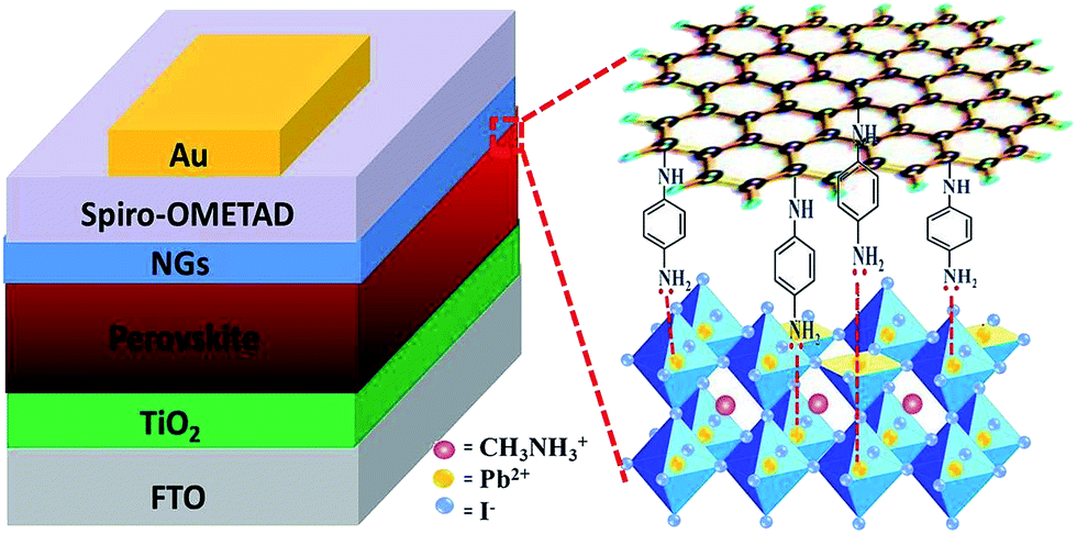 | ||
| Fig. 1 Schematic of the PSCs with the NGs interlayer. | ||
Experimental section
Material preparation
CH3NH3I was synthesized according to the method reported previously in the literature.27 The amino-functionalized graphene (NGs) was prepared by a facial solution process with the phenylenediamine (PPDA) covalently bonded onto the surface of GO, followed by the further chemical reduction with the hydrazine.28 More details on the experimental procedure, morphology and crystalline characterizations as well as the optical and electric measurements are provided in the ESI.†Solar device fabrication
Fluorinated tin oxide glasses (FTO glass, 7 S sq.−1, 85% transmittance in the visible spectrum) partially etched by zinc powder and 2 M hydrochloric acid were cleaned by ultrasonic bath using isopropanol, acetone and DI water in sequence. After exposure to UV-O3 for 15 min, a uniform TiO2 blocking layer was deposited by spin-coating with titanium diisopropoxidebis(acetylacetonate) solution (0.15 M in 1-butanol). After drying at 125 °C for 5 min, the FTO glasses were sintered at 500 °C for 30 min in air. After cooling to room temperature, they were then subjected to 40 mM TiCl4 aqueous solution at 70 °C for 30 min, and washed with DI water adequately. Then, the mesoporous TiO2 film was produced by spin-coating a diluted TiO2 paste (Dyesol DSL18NR-T) with ethanol (2![[thin space (1/6-em)]](https://www.rsc.org/images/entities/char_2009.gif) :7, weight ratio), and calcining at 500 °C for 30 min. A uniform and pinhole-free perovskite (CH3NH3PbI3) layer was deposited onto the above substrate by the Lewis base adduct of PbI2 following the reported method.7 For the interfacial modification, the NGs suspension (0.05 mg mL−1 in chlorobenzene) was drop-coated onto the perovskite under-layer at 2000 rpm for 30 s and 5000 rpm for 20 s. Subsequently, the spiro-OMeTAD-based HTM (30 mg mL−1) without dopants such as Li-TSFI as well as TBP was spin-coated on the CH3NH3PbI3 layer at 4000 rpm for 30 s. Finally, a Au counter-electrode of 100 nm was further thermally evaporated after the device was stored in a desiccator overnight. For comparison, the control device was assembled utilizing the same procedures, except for the NGs interlayer. The active area of the electrode was fixed at 0.014 cm2via the metal mask.
:7, weight ratio), and calcining at 500 °C for 30 min. A uniform and pinhole-free perovskite (CH3NH3PbI3) layer was deposited onto the above substrate by the Lewis base adduct of PbI2 following the reported method.7 For the interfacial modification, the NGs suspension (0.05 mg mL−1 in chlorobenzene) was drop-coated onto the perovskite under-layer at 2000 rpm for 30 s and 5000 rpm for 20 s. Subsequently, the spiro-OMeTAD-based HTM (30 mg mL−1) without dopants such as Li-TSFI as well as TBP was spin-coated on the CH3NH3PbI3 layer at 4000 rpm for 30 s. Finally, a Au counter-electrode of 100 nm was further thermally evaporated after the device was stored in a desiccator overnight. For comparison, the control device was assembled utilizing the same procedures, except for the NGs interlayer. The active area of the electrode was fixed at 0.014 cm2via the metal mask.
Results and discussion
The GO, a precursor for graphene synthesis, contains abundant oxygenated groups, such as epoxy, hydroxyl and carboxylic, in the plane, which not only provide more flexibility for the surface functionalization with other modifiers via the covalent interaction, but also lay a solid foundation for the surface modification of graphene.29 Here, PPDA with two amino groups on the para-position of benzene rings were covalently grafted onto the GO plane via the interaction between the amino groups of PPDA and epoxy groups on the GO basal plane.28 After reduction with the hydrazine monohydrate, graphene with an amino-rich group was developed, and the surface chemical composition was characterized by XPS measurements, as illustrated in Fig. 2A–D and Table S1.† Notably, the appearance of a N peak (Fig. 2A) and C–N bonds (Fig. 2C) as well as –NH– bond (Fig. 2D) and the evidently increased N content (Table S1†) of the resultant NGs suggested that the PPDA was successfully grafted onto the surface, in agreement with the previous result.28 The FTIR measurement, as depicted in Fig. S1,† further confirmed the presence of an amino-rich group on the NGs. In addition, on the basis of the high solution C1s spectrum, compared to that of GO counterpart (Fig. 2B), the contribution from the oxygen-related components (C–O, C (epoxy) and C![[double bond, length as m-dash]](https://www.rsc.org/images/entities/char_e001.gif) O centred at 285.6, 286.7 and 287.2 eV, respectively) decreased significantly, accompanied with an increased C–C peak at 284.6 eV of NGs (Fig. 2C). It was confirmed that the PDDA-modified GO could be further chemically reduced with hydrazine monohydrate effectively. The XRD patterns of the prepared samples are presented in Fig. S2.† Clearly, compared to that of GO, a broad peak can be detected centred at ca. 26° for the NGs along with the disappearance of the sharp (002) diffraction peak at ca. 10°, revealing the efficient reduction of the resultant NGs, which is consistent with the XPS measurement. Therefore, the amino-rich PPDA can serve as an effective modifier for the preparation of amino-functionalized graphene, which lays the foundation for the subsequent surface trap passivation of the perovskite layer.
O centred at 285.6, 286.7 and 287.2 eV, respectively) decreased significantly, accompanied with an increased C–C peak at 284.6 eV of NGs (Fig. 2C). It was confirmed that the PDDA-modified GO could be further chemically reduced with hydrazine monohydrate effectively. The XRD patterns of the prepared samples are presented in Fig. S2.† Clearly, compared to that of GO, a broad peak can be detected centred at ca. 26° for the NGs along with the disappearance of the sharp (002) diffraction peak at ca. 10°, revealing the efficient reduction of the resultant NGs, which is consistent with the XPS measurement. Therefore, the amino-rich PPDA can serve as an effective modifier for the preparation of amino-functionalized graphene, which lays the foundation for the subsequent surface trap passivation of the perovskite layer.
 | ||
| Fig. 2 (A) Full range XPS spectrum of GO and NGs; high-resolution XPS C1s peak of GO (B); high-resolution XPS C1s peak (C) and N1s of NGs (D). | ||
The surface morphologies of different substrates were evaluated by SEM images, as shown in Fig. 3A–C. Clearly, a highly dense CH3NH3PbI3 layer with full coverage was developed by the reported method.7 For use as an interlayer at the perovskite/HTM interface, the NGs suspension was drop-coated onto the perovskite under-layer. Notably, the NGs sheets were successfully deposited in a relatively large domain, and well anchored with the perovskite layer in the horizontal direction in most cases without any negative effect on the crystalline as well as on the optimal property of the perovskite, as revealed by the XRD patterns and UV-Vis spectra (Fig. S3 and S4†). Horizontally laying the NGs ensures a sufficient contact with the perovskite. It has been demonstrated that electron-rich molecules, such as N atoms, can interact with under-coordinated Pb2+ ions of the perovskite by donating electron density, which benefits the efficient surface passivation as well as the charge extraction from the perovskite.30 However, some uncovered perovskite domains and discrete islands of NGs were formed to some extent. However, after the subsequent deposition of HTM, the sub-substrate was fully covered with a continuous dopant-free spiro-OMeTAD layer without the exposed perovskite domain. Moreover, the island NGs were well toughed, in which two-dimensional carbon–carbon bonds of NGs can absorb on the spiro-OMeTAD via π–π interaction, ensuring efficient hole transfer to the back electrode.26
 | ||
| Fig. 3 SEM images of perovskite (A), perovskite/NGs (B) and perovskite/NGs/spiro-OMeTAD (C); (D) cross-sectional SEM image of the resultant device with the architecture of FTO/TiO2 BL/MP-TiO2/perovskite/dopant-free spiro-OMeTAD. | ||
To evaluate the effect of the NGs interlayer on the photovoltaic performance of PSCs, the current density–voltage (J–V) characteristics of the best performing devices (Fig. 3D) were measured under the illumination of AM 1.5G 100 mW cm−2, as illustrated in Fig. 4A, while the corresponding electrical parameters are summarized in the inserted table in the figure. Notably, with the incorporation of an NGs passivation layer at the perovskite/HTM interface, a best efficiency of 14.6% was successfully achieved. Also, the open-circuit voltage (VOC), the short-cut current (JSC), and the fill factor (FF) of the cell were measured as 0.94 V, 23.60 mA cm−2 and 65.81%, respectively, with an average efficiency of 12.64% from the measurements of 10 separate devices (Fig. 4E), which is evidently higher than the devices based on the simple PPDA-modified perovskite layer (Fig. S5†). In comparison, the control device without the NGs interlayer offered a best efficiency of 10.7%, with the VOC, JSC and FF being 0.91 V, 20.8 mA cm−2 and 56.53% respectively, giving an average PCE of 9.57% (Fig. 4E). Clearly, incorporating NGs at the perovskite/HTM interface enabled the devices to achieve a remarkable improvement in the PCE of ca. 36%. In particular, the PCE improvement was mainly related to the increase of JSC and FF, while the VOC underwent a slight increase (Fig. 4B–D).
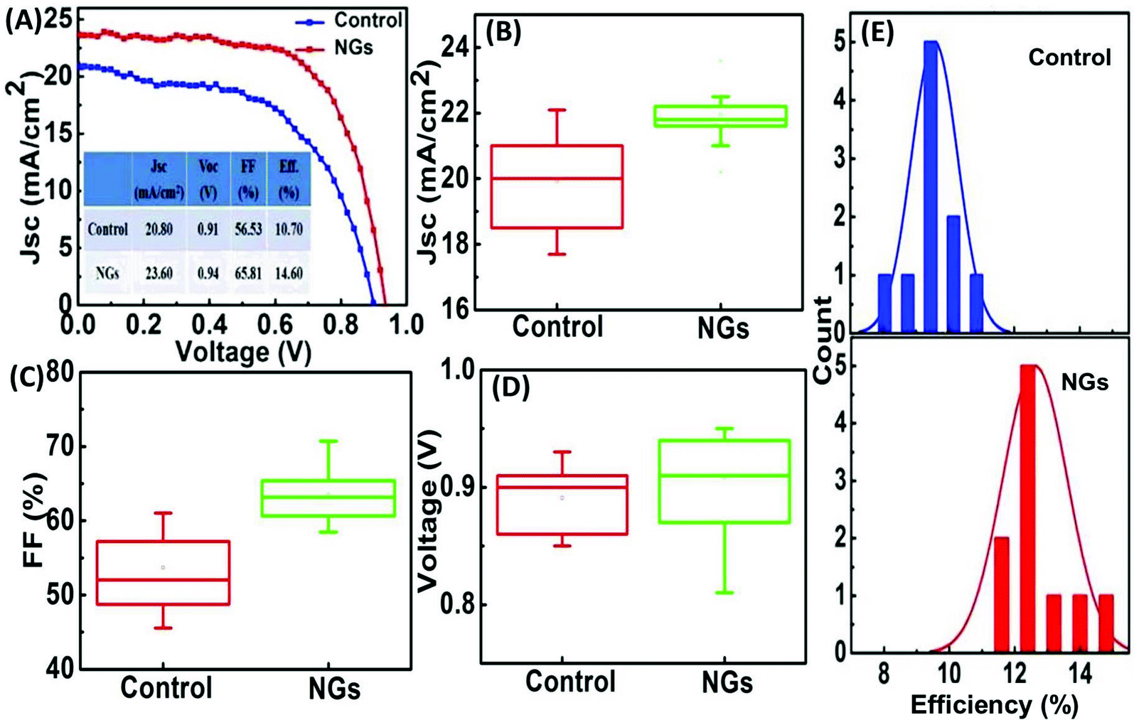 | ||
| Fig. 4 (A) The J–V characteristics of the best cells under the illumination of AM 1.5G 100 mW cm−2 simulated solar light; statistical data of 12 individual devices: (B) short-circuit current density, (C) fill factor and (D) open-circuit voltage; (E) comparison of the PCE distributions of 10 individual devices. | ||
EIS is widely used as a powerful technique to monitor the interfacial change of photovoltaic devices. To reveal the role of the NGs interlayer, we performed EIS measurements in the frequency range from 0.1 Hz to 100 kHz. Fig. 5A presents the Nyquist plots of cells at a bias of 0.9 V in the dark. Generally, the arc at the high frequency is associated with the contact resistance at the HTM/Au interface, while the lower frequency one is ascribed to the recombination resistance (Rrec) and chemical capacitance of the cells.31,32 The Rrec, which is the diameter of the main semicircle, indicates the recombination behaviour of the electrons from the perovskite/TiO2 with the HTM. The increased radius is related with the improved recombination resistance, which benefits the reduced charge recombination at the perovskite/HTM interface. Clearly, based on the NGs interlayer, the recombination resistance of the devices was evidently improved in comparison with the control devices, suggesting the efficient blocking of the charge recombination. Also, a higher built-in potential was obtained for NGs-modified PSCs, which provided an enhanced driving force for the separation of photogenerated carriers, as revealed by the Mott–Schottky plots (Fig. S6†). Consequently, more photogenerated holes could transport through the NGs to the spiro-OMeTAD. So, the incorporated NGs was able to serve as an effective hole extraction and transfer pathway, in accordance with previous reports.24 Moreover, the transient open-circuit voltage (VOC) decay as a function of time was demonstrated to be an effective way to monitor the charge recombination kinetics of PSCs.33,34 Generally, once turning off the illumination, the VOC will decay sharply due to the photo-carrier recombination, and so the VOC–decay rate directly indicates the charge recombination rate. To further verify the positive role of NGs on the hole control from the perovskite to HTM, VOC–decays curve were plotted in Fig. 5B. Clearly, the PSCs with the NGs interlayer exhibited an evidently slower VOC decay rate than the control, suggesting a suppressed charge recombination. The electron lifetime (τn) was extracted by τn = −(kBT/e)(dVOC/dt)−1,35 which is the average time that the photogenerated electrons exist before they recombine, and was plotted as a function of VOC, as depicted in the inset of Fig. 5B. As expected, with the NGs at the perovskite/HTL interface, the device achieved an improved τn at any chosen VOC, which directly reflected the reduced photo-carrier recombination. Moreover, the hole-quenching ability of NGs was further probed by the PL spectra, as illuminated in Fig. 5C. Under the same experimental conditions, both films displayed PL peaks at 760 nm arising from the perovskite layer. Generally, the PL quenching is supposed to originate from the efficient charge-carrier extraction across the interfaces, and a dramatic PL quenching is expected for the reduced photo-carrier combination. Clearly, after the insertion of the NGs, an evidently reduced PL emission was observed compared to the control device. Such remarkable PL quenching indicated that NGs can also act as an effective bridge to enhance the hole extraction and injection from the perovskite to HTM. In addition, the PL measurement was also demonstrated to be an effective way to study the surface trap states on the perovskite surface or grain boundary. Generally, filling the surface trap can induce a blue shift of the PL peak, resulting from the recovery of the bandgap.36 Therefore, we performed PL measurements to study the trap passivation effect of NGs with the structure of FTO/TiO2 BL/MP-TiO2/perovskite/NGs/spiro-OMeTAD. Clearly, the control device exhibited a strong PL peak centred at 775 nm. After the surface engineering with the NGs, the PL peak was shifted to 772 nm for the perovskite films. The slight blue-shifted PL peak can be ascribed to the reduced surface traps of the perovskite, resulting from the coordinate or dative-covalent bond between amines on the graphene and the under-coordinated Pb2+ on the perovskite surface.30 Therefore, the incorporated NGs not only enhanced the hole behaviour at the perovskite/HTM interface, but also passivated the surface traps of the perovskite, which both improve benefited the photovoltaic performance (Fig. 5D).
 | ||
| Fig. 5 (A) Nyquist plots in the dark condition and (B) the VOC–decay curve (the inset: the extracted τn–decay curve) of resultant devices; (C) steady-state PL spectra of perovskite/spiro-OMeTAD and perovskite/NGs/spiro-OMeTAD film excited by a 520 nm light source; (D) schematic illustration of perovskite/HTM interface. | ||
Conclusions
In this work, amino-rich graphene (NGs) was developed from a facial solution method as a functionalized interlayer at the perovskite/HTM interface. The interfacial modification with the NGs interlayer facilitated the hole extraction and transfer from the perovskite to spiro-OMeTAD, and led to reduced surface traps on the perovskite layer as revealed by EIS in the dark as well as by PL measurements. With such an interfacial modification, the best PCE of 14.6% was achieved for the PSCs fabricated under ambient conditions. This work demonstrated an effective strategy of the application of interfacial engineering application surface-modified graphene derivatives for efficient perovskite solar cells.Acknowledgements
The authors gratefully acknowledge the financial support from the National Basic Research Program of China (2012CB932900), and the National Natural Science Foundation of China (21321062). Xiaoru Wen acknowledges the financial support from the China Scholarship Council.Notes and references
- A. Kojima, K. Teshima, Y. Shirai and T. Miyasaka, J. Am. Chem. Soc., 2009, 131, 6050–6051 CrossRef CAS PubMed.
- W. S. Yang, J. H. Noh, N. J. Jeon, Y. C. Kim, S. Ryu, J. Seo and S. I. Seok, Science, 2015, 348, 1234–1237 CrossRef CAS PubMed.
- G. Hodes, Science, 2013, 342, 317–318 CrossRef CAS PubMed.
- M. M. Lee, J. Teuscher, T. Miyasaka, T. N. Murakami and H. J. Snaith, Science, 2012, 338, 643–647 CrossRef CAS PubMed.
- G. Xing, N. Mathews, S. Sun, S. S. Lim, Y. M. Lam, M. Gratzel, S. Mhaisalkar and T. C. Sum, Science, 2013, 342, 344–347 CrossRef CAS PubMed.
- H. J. Snaith, J. Phys. Chem. Lett., 2013, 4, 3623–3630 CrossRef CAS.
- N. Ahn, D.-Y. Son, I.-H. Jang, S. M. Kang, M. Choi and N.-G. Park, J. Am. Chem. Soc., 2015, 137, 8696–8699 CrossRef CAS PubMed.
- P. W. Liang, C. Y. Liao, C. C. Chueh, F. Zuo, S. T. Williams, X. K. Xin, J. Lin and A. K. Jen, Adv. Mater., 2014, 26, 3748–3754 CrossRef CAS PubMed.
- M. Liu, M. B. Johnston and H. J. Snaith, Nature, 2013, 501, 395–398 CrossRef CAS PubMed.
- W. Peng, B. Anand, L. Liu, S. Sampat, B. E. Bearden, A. V. Malko and Y. J. Chabal, Nanoscale, 2016, 8, 1627–1634 RSC.
- A. Abate, M. Saliba, D. J. Hollman, S. D. Stranks, K. Wojciechowski, R. Avolio, G. Grancini, A. Petrozza and H. J. Snaith, Nano Lett., 2014, 14, 3247–3254 CrossRef CAS PubMed.
- N. K. Noel, A. Abate, S. D. Stranks, E. S. Parrott, V. M. Burlakov, A. Goriely and H. J. Snaith, ACS Nano, 2014, 8, 9815–9821 CrossRef CAS PubMed.
- L. Kavan, J.-H. Yum and M. Graetzel, Phys. Status Solidi B, 2013, 250, 2643–2648 CrossRef CAS.
- Y. Yang, C. Han, B. Jiang, J. Iocozzia, C. He, D. Shi, T. Jiang and Z. Lin, Mater. Sci. Eng., R, 2016, 102, 1–72 CrossRef.
- H. Sung, N. Ahn, M. S. Jang, J.-K. Lee, H. Yoon, N.-G. Park and M. Choi, Adv. Energy Mater., 2015, 6, 1501873–1501879 CrossRef.
- P. You, Z. Liu, Q. Tai, S. Liu and F. Yan, Adv. Mater., 2015, 27, 3632–3638 CrossRef CAS PubMed.
- J. T. Wang, J. M. Ball, E. M. Barea, A. Abate, J. A. Alexander-Webber, J. Huang, M. Saliba, I. Mora-Sero, J. Bisquert, H. J. Snaith and R. J. Nicholas, Nano Lett., 2014, 14, 724–730 CrossRef CAS PubMed.
- G. S. Han, Y. H. Song, Y. U. Jin, J. W. Lee, N. G. Park, B. K. Kang, J. K. Lee, I. S. Cho, D. H. Yoon and H. S. Jung, ACS Appl. Mater. Interfaces, 2015, 7, 23521–23526 CAS.
- D. Y. Lee, S. I. Na and S. S. Kim, Nanoscale, 2016, 8, 1513–1522 RSC.
- A. Agresti, S. Pescetelli, L. Cinà, D. Konios, G. Kakavelakis, E. Kymakis and A. D. Carlo, Adv. Funct. Mater., 2016, 26, 2686–2694 CrossRef CAS.
- M. Acik and S. Darling, J. Mater. Chem. A, 2016, 4, 6185–6235 CAS.
- Z. Wu, S. Bai, J. Xiang, Z. Yuan, Y. Yang, W. Cui, X. Gao, Z. Liu, Y. Jin and B. Sun, Nanoscale, 2014, 6, 10505–10510 RSC.
- S. N. Habisreutinger, T. Leijtens, G. E. Eperon, S. D. Stranks, R. J. Nicholas and H. J. Snaith, Nano Lett., 2014, 14, 5561–5568 CrossRef CAS PubMed.
- Q. Luo, Y. Zhang, C. Liu, J. Li, N. Wang and H. Lin, J. Mater. Chem. A, 2015, 3, 15996–16004 CAS.
- J. Xiao, J. Shi, H. Liu, Y. Xu, S. Lv, Y. Luo, D. Li, Q. Meng and Y. Li, Adv. Energy Mater., 2015, 5, 1401943–1401950 CrossRef.
- W. Li, H. Dong, X. Guo, N. Li, J. Li, G. Niu and L. Wang, J. Mater. Chem. A, 2014, 2, 20105–20111 CAS.
- J. H. Heo, S. H. Im, J. H. Noh, T. N. Mandal, C. Lim, J. A. Chang, Y. H. Lee, H. Kim, A. Sarkar, M. K. Nazeeruddin, M. Grätzel and S. I. Seok, Nat. Photonics, 2013, 7, 486–491 CrossRef CAS.
- X. Lu, L. Li, B. Song, K. Moon, N. Hu, G. Liao, T. Shi and C. Wong, Nano Energy, 2015, 17, 160–170 CrossRef CAS.
- A. B. Bourlinos, D. Gournis, D. Petridis, T. Szabó, A. Szeri and I. Dékány, Langmuir, 2003, 19, 6050–6055 CrossRef CAS.
- C. Sun, Z. Wu, H.-L. Yip, H. Zhang, X.-F. Jiang, Q. Xue, Z. Hu, Z. Hu, Y. Shen, M. Wang, F. Huang and Y. Cao, Adv. Energy Mater., 2015, 6, 1501534–1501544 CrossRef.
- P. P. Boix, Y. H. Lee, F. Fabregat-Santiago, S. H. Im, I. Mora-Sero, J. Bisquert and S. I. Seok, ACS Nano, 2012, 6, 873–880 CrossRef CAS PubMed.
- I. Morá-Seró, J. Bisquert, F. Fabregat-Santiago and G. Garcia-Belmonte, Nano Lett., 2006, 6, 640–650 CrossRef PubMed.
- M. L. Jiang, J. M. Wu, F. Lan, Q. Quan Tao, D. Di Gao and G. Y. Li, J. Mater. Chem. A, 2015, 3, 963–967 CAS.
- A. Pockett, G. E. Eperon, T. Peltola, H. J. Snaith, A. Walker, L. M. Peter and P. J. Cameron, J. Phys. Chem. C, 2015, 119, 3456–3465 CAS.
- J. Bisquert, A. Zaban, M. Greenshtein and I. Mora-Sero, J. Am. Chem. Soc., 2004, 126, 13550–13559 CrossRef CAS PubMed.
- Y. Shao, Z. Xiao, C. Bi, Y. Yuan and J. Huang, Nat. Commun., 2014, 5, 5784–5791 CrossRef CAS PubMed.
Footnote |
| † Electronic supplementary information (ESI) available: Details of experimental procedure, XRD, FTIR and UV-Vis spectra for different substrates. See DOI: 10.1039/c6ta04616a |
| This journal is © The Royal Society of Chemistry 2016 |