
 Open Access Article
 This Open Access Article is licensed under a Creative Commons Attribution-Non Commercial 3.0 Unported Licence
Effects of interfacial layers on the photoelectrochemical properties of tantalum nitride photoanodes for solar water splitting†
Chizhong
Wang
a,
Takashi
Hisatomi
ab,
Tsutomu
Minegishi
 abc,
Mamiko
Nakabayashi
d,
Naoya
Shibata
d,
Masao
Katayama
ab and
Kazunari
Domen
*ab
abc,
Mamiko
Nakabayashi
d,
Naoya
Shibata
d,
Masao
Katayama
ab and
Kazunari
Domen
*ab
aDepartment of Chemical System Engineering, School of Engineering, The University of Tokyo, 7-3-1 Hongo, Bunkyo-ku, 113-8656 Tokyo, Japan. E-mail: domen@chemsys.t.u-tokyo.ac.jp; Fax: +81 3 5841 8838; Tel: +81 3 5841 1148
bJapan Technological Research Association of Artificial Photosynthetic Chemical Process (ARPChem), 2-11-9 Iwamotocho, Chiyoda-ku, 101-0032 Tokyo, Japan
cJapan Science and Technology Agency/Precursory Research for Embryonic Science and Technology (JST/PRESTO), Kawaguchi Center Building, 4-1-8, Honcho, Kawaguchi-shi, 332-0012 Saitama, Japan
dInstitute of Engineering Innovation, The University of Tokyo, 2-11-16 Yayoi, Bunkyo-ku, 113-8656 Tokyo, Japan
First published on 9th August 2016
Abstract
This work describes the effects of interlayers on the structural, crystalline and photoelectrochemical properties of Ta3N5 photoanodes. Nb4N5 interlayers with different thicknesses are formed between Ta3N5 films and Ta back substrates using a thin film transfer method. Zone-axis images and electron diffraction patterns of cross-sections of the resulting Ta3N5/Nb4N5/Ta/Ti electrodes acquired by transmission electron microscopy evidence the formation of a 200 nm thick oriented Ta3N5 grain layer in the vicinity of the interlayer. This oriented Ta3N5 layer promotes electron transport throughout the Ta3N5 film. As a result, a Ta3N5 photoanode incorporating a Nb4N5 interlayer exhibits a higher photocurrent during the oxygen evolution reaction. These results obtained using the Ta3N5/interlayer/substrate configuration elucidate the key role played by the buffer layer in achieving efficient water splitting with Ta3N5 photoelectrodes.
Introduction
Photoelectrochemical (PEC) water splitting is a process used to store solar light energy via the formation of hydrogen.1–3 Ta3N5, an n-type semiconductor, has been widely applied as a photoanode for the PEC oxygen evolution reaction (OER). With a bandgap of 2.1 eV, Ta3N5 absorbs visible light up to 600 nm (ref. 4) and can potentially yield a maximum photocurrent of 12.5 mA cm−2 under irradiation by sunlight (AM 1.5G).Photoanodes are typically prepared as either thin films,5 nanostructures (such as nanorods and nanotubes)6–8 or particulate layers.9,10 In addition, doping, surface modification and other strategies have been applied to achieve high photocurrents and negative onset potentials during PEC water oxidation.11–16 Theoretical studies have indicated that Ta3N5 is an anisotropic semiconductor material in which holes are heavier than electrons,17 resulting in low mobility of the minority charge carriers (i.e., the holes), while the porosity of the Ta3N5 layer in a Ta3N5 photoanode is believed to limit the bulk transport of the majority charge carriers (electrons).18 Controlling both the structure and crystallinity of Ta3N5 films is a critical aspect of improving the PEC performance of this material because these parameters significantly affect the charge separation efficiency as well as the light absorption of the Ta3N5.17–20
Studies on the growth of GaN films suggest that a GaN or AlN buffer layer will generate high crystalline quality in the upper GaN film,21,22 and a similar effect is anticipated in the case of Ta3N5 film growth. In order to fabricate semiconductor/conductor configurations for use as photoelectrodes, Ta3N5 films are generally grown on conductive substrates, such as metallic Ta foils or Pt,23 by nitridation under a flow of NH3 gas and at high temperatures (800–1000 °C). To date, Ta3N5 photoanodes with state-of-the-art PEC performance have been fabricated on Ta foil substrates.11,24 However, an impurity interlayer consisting of TaNx phases is inevitably formed between the Ta3N5 film (or nanorods and nanotubes) and the underlying Ta foil during the nitridation process.6,20 The effects of this interlayer on electron transport in the Ta3N5 film and at the Ta3N5/TaNx interface are expected to alter the PEC performance of Ta3N5 photoanodes.
In the present work, the effects of interlayers on the growth of Ta3N5 films and on the PEC performance of Ta3N5 photoanodes were assessed by introducing a niobium nitride (NbNx) layer at the interface between the Ta3N5 film and the conductive substrate by a thin film transfer technique.25 Inert Si wafers were used as synthesis platforms for the formation of the NbNx and Ta3N5 bilayer films. After the film transfer process, the NbNx surface layer acted as a back contact to conduct photogenerated electrons from the Ta3N5 film to the back conductive layer, and the introduction of a NbNx interlayer was found to enhance the photocurrent of the Ta3N5 photoanodes. The growth mechanism of the Ta3N5 films in the presence of the NbNx layer and the effects of the interlayer on the structural, crystalline and PEC properties of the Ta3N5 films are discussed based on the results of this study.
Experimental section
Sample preparation
A NbNx layer was introduced as an interlayer between Ta3N5 and a conductive substrate using a film transfer process, as depicted in Fig. 1. The sections of a single-crystal Si (100) substrate (1 × 1 cm, Nilaco) were cleaned by sequential ultrasonic irradiation over 10 min each in acetone, isopropanol and Milli-Q water (18.2 mΩ cm). Ta and Nb films with the desired thicknesses were sequentially deposited on the Si substrates by radio frequency (RF) magnetron sputtering (ULVAC, MNS-2000-RFG3) and the resulting multi-layered films were oxidized in a muffle furnace at 700 °C for 2 h with a temperature ramp rate of 15 °C min−1. The Nb2O5/Ta2O5/Si samples fabricated in this manner were subsequently moved to a tube furnace and nitrided in a flow of NH3 gas (100 sccm) at 900 °C for 2 h with a temperature ramp rate of 20 °C min−1, forming a nitride bilayer on the Si substrates. To transfer these nitride films onto a conductive substrate, metallic Ta (150 nm) and Ti (approximately 5 μm) layers were sequentially deposited on the NbNx/Ta3N5/Si sample by RF magnetron sputtering, serving as the contact and conductive layers, respectively. Because the physical contact between the Ta3N5 film and the Si substrate was weakened by the strain imparted upon adding the metallic Ta/Ti layers, the Ti/Ta/NbNx/Ta3N5 films were readily peeled away from the underlying Si substrate using carbon tape supported with glass plates. For comparison purposes, a Ta3N5/Ta/Ti film without a NbNx interlayer was synthesized in the same manner. The electrode areas exposed to the electrolyte solution were approximately 0.2 cm2. Each of the Ta3N5 films used in this work was 630 nm thick, while the thickness of the NbNx layer varied from 50 to 200 nm. | ||
| Fig. 1 Schematic diagram of the procedure used to synthesize a Ta3N5 film with a NbNx interlayer. (i) Sputtering of Ta and Nb metallic films, (ii) oxidation and nitridation of the Ta/Nb films, (iii) sputtering of Ta/Ti metallic layers, and (iv) exfoliation of the NbNx/Ta3N5 films from the Si substrate. | ||
Characterization
Scanning electron microscopy (SEM, S-4700, Hitachi), transmission electron microscopy and scanning transmission electron microscopy (TEM, STEM, JEM-2800, JEOL) with energy dispersive X-ray fluorescence spectroscopy (EDX, EX-24055JGT, JEOL) were used to characterize the morphologies and structures of the thin films. Samples for cross-sectional SEM and STEM assessments were prepared by ion milling and focused ion beam (FIB) milling, respectively. X-ray diffraction (XRD) patterns were recorded using an X-ray diffractometer (Rigaku Ultima III) with Cu Kα radiation (λ = 0.15405 nm, 40 mV and 40 mA). The average crystallite size in the Ta3N5 films (n = 3, ±σ) was calculated using the Scherrer equation. X-ray fluorescence spectroscopy (XPS, JEOL, JPS-90SX) was performed using Mg Kα radiation (8 kV and 10 mA), employing the C 1s peak at 284.8 eV as an internal standard to calibrate the binding energies.Electrochemical measurement
Prior to the PEC measurements, each Ta3N5 photoelectrode was deposited with a thin layer of Co(OH)x using an impregnation method. This was accomplished by adding an aqueous NaOH solution (50 mM, 2.5 mL) to an aqueous Co(NO3)2 solution (6.3 mM, 10 mL) and immersing the Ta3N5 electrodes in the mixture for 1 h. The PEC properties of the Ta3N5 photoanodes were measured using a three-electrode cell with a Ag/AgCl reference electrode (in saturated aqueous KCl) and Pt wire as the counter electrode. The Ag/AgCl reference potential was converted to the reversible hydrogen electrode (RHE) potential according to the Nernst relationship| E (V vs. RHE) = E (V vs. Ag/AgCl) + 0.059 × pH + 0.197, | (1) |
The incident photon-to-current conversion efficiency (IPCE) was measured under monochromatic irradiation from a Xe lamp (MAX-302, Asahi Spectra) in a 0.5 M KPi electrolyte. The wavelength-dependent IPCEs were calculated using the equation
| IPCE = 1240 × (Ilight − Idark)/(λ × Pinput) × 100% | (2) |
To compare the relative electrochemically active surface areas and roughness factors of different Ta3N5 photoelectrodes, the scan-rate dependencies of cyclic voltammograms were estimated according to a previously reported method.26 All of the electrodes were tested at different scan rates, varying from 5 to 300 mV s−1, with a capacitive current estimated at −0.1 V vs. Ag/AgCl. Mott–Schottky measurements were performed in a 0.5 M KPi electrolyte at a frequency of 1000 Hz with an AC amplitude of 10 mV, using an impedance analyzer (METEK, VersaSTAT3-200). The flat band potential and donor dopant density values of the Ta3N5 photoanodes were determined according to the Mott–Schottky relationship
 | (3) |
Results and discussion
Structure and crystallinity
A top-view SEM image of a Ta3N5/NbNx/Ta/Ti sample after the thin film transfer is shown in Fig. 2(a). The surface of the Ta3N5 film exhibits roughness originating from the porous contact at the Ta3N5/Si interface in the parent NbNx/Ta3N5/Si sample. The possible exposure of the NbNx interlayer to the film surface is ruled out by the XPS data obtained from the Ta3N5/NbNx/Ta/Ti film, as shown in Fig. S1.† In addition, the absence of Ta species on the surface of the parent NbNx/Ta3N5/Si sample suggests that the Ta3N5 film was not in direct contact with the underlying metallic substrate. The layered structure of the Ta3N5/NbNx/Ta/Ti sample is clearly observed in the cross-sectional SEM image presented in Fig. 2(b). Here, the NbNx layer is evident as a region of darker contrast, with a thickness of approximately 100 nm. In the magnified view, a porous structure is observed throughout the Ta3N5/NbNx film, due to the oxidation of the metallic film and the substitution of O2− ions by N3− ions during the nitridation process, just as occurs during the nitridation of Ta2O5 powder to Ta3N5. Despite its porous structure, the NbNx layer is in intimate contact with the Ta3N5 film and the Ta contact layer. The EDX mapping images (Fig. 3) demonstrate that the distribution of Nb was confined to the interlayer region, so there was no appreciable doping of Nb into the Ta3N5 film. | ||
| Fig. 2 (a) Top-view and (b) cross-sectional SEM images of a Ta3N5/NbNx/Ta/Ti film. The scale bars are (a) 5 μm, (b) 500 nm, and 100 nm for the zoomed image. | ||
 | ||
| Fig. 3 (a) Cross-sectional STEM image of a Ta3N5/NbNx/Ta/Ti film and (b)–(e) EDX elemental mappings of the image in (a). All scale bars are 500 nm. | ||
Fig. 4 presents the XRD patterns of NbNx/Ta3N5/Si samples with different NbNx thicknesses prior to the thin film transfer, as a means of confirming the nitridation products. A Ta3N5 phase was evidently formed regardless of whether a NbNx layer was present or not. In addition, impurity phases such as TaNx or SiNx were absent. The diffraction pattern of the NbNx layer deposited on a Si substrate (Fig. 4(e)) suggests that Nb4N5 was the main phase formed in the NbNx/Ta3N5/Si sample, although the crystallinity of this specimen was low, and the diffraction peaks of the (101) and (211) planes of the Nb4N5 overlap with those generated by the (110) and (113) planes of the Ta3N5 at 24.4° and 36.0°, respectively. A peak attributable to NbNx (x ≤ 1) was also detected at 34.0° when the thickness of the NbNx layer was at its maximum (200 nm). Nevertheless, the XRD peaks obtained from the NbNx/Ta3N5/Si primarily provide information regarding the Ta3N5 phase because the Ta3N5 peaks are much stronger than those generated by the Nb4N5 and other NbNx phases. It should also be noted that Nb3N5 was not observed, as expected because Nb5+ is prone to reduction to Nb4+ or lower-valence nitride species.27
 | ||
| Fig. 4 XRD patterns of (a) Ta3N5/Si, (b)–(d) NbNx/Ta3N5/Si with NbNx thicknesses of (b) 50, (c) 100, and (d) 200 nm, and (e) NbNx (100 nm)/Si samples. XRD patterns of Nb4N5 (PDF# 74-0606) and Ta3N5 (PDF# 79-1533) are presented at the bottom and the top, respectively, as references. | ||
The crystallite sizes of the Ta3N5 films were calculated from the (110) diffraction peak at 24.4°. The data in Table 1 demonstrate that each of the Ta3N5 films had almost identical average crystallite sizes, in the range of 40–45 nm. Thus, the effect of the NbNx layer on the crystallite size in the Ta3N5 film was not significant. Notably, the intensity ratio (Rin) obtained from the peaks at 24.4° and 36.0°, which correspond to the (110) and (113) planes of Ta3N5, decreased from 2.4 to 0.5–0.8 when NbNx layers were present on the Ta3N5 films.
| NbNx thickness (nm) | Crystallite size (nm) | Peak intensity ratio |
|---|---|---|
| 0 | 42.6 ± 1.8 | 2.4 ± 0.2 |
| 50 | 44.3 ± 1.8 | 0.5 ± 0.1 |
| 100 | 41.8 ± 4.4 | 0.7 ± 0.2 |
| 200 | 42.0 ± 2.7 | 0.8 ± 0.1 |
The crystalline growth of each Ta3N5 film was examined in detail by acquiring cross-sectional TEM images of Ta3N5/NbNx films (Fig. 5). These bright field (BF) zone-axis TEM images provide a clear view of the multi-layered structure of the Ta3N5/NbNx/Ta samples, and the bright spots scattered within the darker contrast can provide information regarding the sizes and boundaries of individual grains. In Fig. 5(a) and (b), a high density of bright spots is observed throughout the 100 nm-thick NbNx interlayer, suggesting that the grain size of the NbNx phase was much less than the layer thickness of 100 nm (likely below 10 nm). This result agrees with the low-crystalline Nb4N5 phase indicated by the XRD patterns in Fig. 4. Notably, the Ta3N5 region close to the Ta3N5/NbNx interface generated fewer bright spots when over 200 nm in thickness, as shown in Fig. 5(c), indicating the presence of fewer boundaries among the Ta3N5 grains near the interface with the NbNx layer, while the rest of the Ta3N5 film exhibited a number of bright spots.
 | ||
| Fig. 5 (a) Zone-axis TEM images of the cross-section of a Ta3N5 film on a Ta/Ti substrate with a NbNx interlayer. The region (200 nm thick) within the white dashed lines represents the oriented Ta3N5 layer. SAED patterns of Ta3N5 crystallinites near (b) the surface of the Ta3N5 film, and (c) the interface of the Ta3N5/NbNx. The insets are diffraction patterns from the selected regions highlighted by the circles. All scale bars are 200 nm. | ||
Selected area electron diffraction (SAED) patterns taken from the regions at 100 nm to the film surface and 100 nm to the Ta3N5/NbNx interface are displayed in the insets of Fig. 5(b) and (c), respectively. The Ta3N5 near the interface with the NbNx generated a more ordered diffraction pattern compared to the Ta3N5 close to the surface, which was characterized by random diffractions. This finding indicates that the arrangement of the Ta3N5 grains was well oriented in the vicinity of the NbNx interlayer. It should be noted that crystallite orientation was not observed at the interface between the Ta3N5 film and the Ta/Ti substrate of the Ta3N5/Ta/Ti film without a NbNx interlayer, as seen in Fig. S2.†
As suggested by the SAED pattern, the formation of a highly oriented 200 nm Ta3N5 layer is not continuous throughout the entirety of the 630 nm Ta3N5 film. The growth mode of the Ta3N5 film in the presence of the NbNx interlayer appears to be consistent with that observed for Ta3N5 films directly grown on Ta foil substrates by thermal nitridation, as reported by Pinaud et al.18 The electrochemically active surface areas (ECSAs) of the Ta3N5 films fabricated by Pinaud's group were found to exhibit minimal change up to a film thickness of 260 nm due to the growth of a compact Ta3N5 film. However, the ECSA increased by one or two orders of magnitude when the film thickness was increased from 260 to 630 nm, owing to the growth of disordered layers over top of the compact Ta3N5 films. The formation of an oriented Ta3N5 layer was also observed in the present Ta3N5 films grown on Ta foil substrates (Fig. S3†). Therefore, it is believed that both Ta3N5 films grown on Ta substrates and films nitrided in contact with a NbNx interlayer have similar growth mechanisms, presumably involving Ta4N5 and Nb4N5 with the same crystal structures28,29 acting as interlayers, respectively.
Photoelectrochemical properties
Current–potential curves obtained from the Ta3N5 film photoelectrodes deposited with a layer of Co(OH)x as an OER catalyst are shown in Fig. 6(a). In the absence of the NbNx interlayer, the Ta3N5 photoelectrode exhibited an anodic photocurrent of approximately 2.0 mA cm−2 at 1.23 V vs. RHE. The photocurrent densities increased significantly for the Ta3N5 films with NbNx interlayers 50–100 nm in thickness. However, the higher resistance of the NbNx (Nb4N5) interlayer compared to that of the metallic Ta substrate lowered the electron mobility. As a result, the photocurrent decreased as the thickness of the NbNx interlayer was increased from 100 to 200 nm. Moreover, the onset potential of the photoanodic current generated by the Ta3N5/NbNx (100 nm)/Ta/Ti electrode shifted cathodically by 0.1 V from 0.9 V vs. RHE relative to the Ta3N5/Ta/Ti electrode. The NbNx (Nb4N5 or NbN) phase acts as a conductive contact for the transport of the majority charge carriers (electrons) collected from the Ta3N5 film. | ||
| Fig. 6 (a) Current–potential curves obtained from Ta3N5/Ta/Ti and Ta3N5/NbNx/Ta/Ti photoelectrodes with different NbNx interlayer thicknesses, (b) hydrogen and oxygen gas evolution with respect to the total charge passed, as calculated from the (c) current–time curve obtained from the Co(OH)x/Ta3N5/NbNx (100 nm)/Ta/Ti photoelectrode held at 1.0 V vs. RHE. The PEC activities and gas evolution were assessed in a 0.5 M potassium phosphate solution (pH 13) under simulated AM 1.5G light. | ||
To confirm that the enhancement of the photocurrent of Ta3N5/NbNx photoanodes is associated with the PEC water oxidation performance, gaseous H2 and O2 evolved at the counter electrode and the photoanode at 1.0 V vs. RHE were analyzed using a micro gas chromatograph (Fig. 6(b)). It was confirmed that the amounts of H2 and O2 were virtually equal to the values calculated based on the total charge passed through the system. In addition, the ratio of H2 to O2 was close to 2![[thin space (1/6-em)]](https://www.rsc.org/images/entities/char_2009.gif) :1. These results indicate that the faradaic efficiency during the OER process was unity when employing the Ta3N5/NbNx photoanode. However, the gas evolution rates decreased in accordance with changes in the photocurrent over time, as can be seen in Fig. 6(c). The decreased photocurrent and O2 evolution rate likely resulted from dissolution of the Co-based catalysts from the surface of the Ta3N5 film into the electrolyte solution.30 The loss of the Co-based catalyst led to direct exposure of the Ta3N5 film to the electrolyte solution, and consequently to gradual degradation of the photoanode because bare Ta3N5 photoanodes are prone to photocorrosion.31 A uniform coverage of the Ta3N5 electrode with protective and catalytic layers is likely to stabilize the photocurrent. In addition, the Co-based catalyst can be replaced by other oxygen-evolution catalysts (e.g. NiOx), which are electrochemically stable against the dissolution under alkaline conditions.
:1. These results indicate that the faradaic efficiency during the OER process was unity when employing the Ta3N5/NbNx photoanode. However, the gas evolution rates decreased in accordance with changes in the photocurrent over time, as can be seen in Fig. 6(c). The decreased photocurrent and O2 evolution rate likely resulted from dissolution of the Co-based catalysts from the surface of the Ta3N5 film into the electrolyte solution.30 The loss of the Co-based catalyst led to direct exposure of the Ta3N5 film to the electrolyte solution, and consequently to gradual degradation of the photoanode because bare Ta3N5 photoanodes are prone to photocorrosion.31 A uniform coverage of the Ta3N5 electrode with protective and catalytic layers is likely to stabilize the photocurrent. In addition, the Co-based catalyst can be replaced by other oxygen-evolution catalysts (e.g. NiOx), which are electrochemically stable against the dissolution under alkaline conditions.
The IPCE spectra shown in Fig. 7 are consistent with the increases in photocurrent densities brought about by the NbNx interlayers (see Fig. 6(a)). The onset of a photoresponse at 600 nm corresponds to the direct band gap of Ta3N5 at 2.1 eV. It should be noted that a shoulder is observed at 500 nm in each of the IPCE plots. This is also ascribed to the direct transition of Ta3N5 between the N 2p and Ta 5d states, as was suggested by earlier optical and theoretical studies of Ta3N5 films.17,32 The IPCEs of Ta3N5/NbNx photoelectrodes at 400–550 nm were evidently increased compared to the bare Ta3N5 photoelectrode. Because less than 5% of light can traverse through the Ta3N5 film to the NbNx interlayer below 550 nm (see Fig. S4†), it is unlikely that the photoresponse of the Ta3N5/NbNx electrode was affected by the light absorption characteristics of the NbNx interlayer and the Ta3N5/NbNx interface. Therefore, it is thought that the enhancements in the IPCE and the photocurrent density of the Ta3N5/NbNx photoelectrodes are primarily due to the changes in the structural features of the Ta3N5 film induced by the NbNx interlayer.
 | ||
| Fig. 7 IPCE spectra of Ta3N5/Ta/Ti and Ta3N5/NbNx/Ta/Ti photoelectrodes with different NbNx interlayer thicknesses. | ||
Charge separation and transport
In the PEC water oxidation process, light harvesting, charge separation and transport, and hole injection are the three key processes that define the PEC activity and IPCE. The light harvesting of the Ta3N5 films would not be expected to have been altered by the NbNx interlayers because the film thickness and crystallite size were unchanged. It is also believed that the hole injection process was not affected by the presence of the interlayer because of the similarities in the roughness factors, flat band potentials, and donor densities. ECSA values were estimated from the double-layer charging in the cyclic voltammograms (CVs) as a means of examining the surface roughness of the Ta3N5 electrodes (Fig. S5†), and the roughness factor was found to be barely changed by the presence of the NbNx interlayer. Mott–Schottky plots (Fig. S6†) were used to estimate the flat band potentials and the carrier densities, with values of −0.06 and −0.08 V vs. RHE, respectively. Hence, charge separation and transport are evidently the major factors contributing to the enhancement of the photocurrent by the NbNx interlayer. Electrochemical impedance spectra (EIS) of Ta3N5 and Ta3N5/NbNx electrodes are shown in Fig. 8. The Nyquist plots with a feature of single capacitance were fitted using the Randles equivalent circuit model, similar to the case for hematite photoanodes in the presence of [Fe(CN)6]3−/4− redox couples.33 This equivalent circuit consists of the series resistance (Rs) of the NbNx and Ta/Ti layers, the capacitance of the bulk Ta3N5 film (CPE), and the charge transfer resistance from the valence band of Ta3N5 to the solution (RCT), which may be associated with resistances representing bulk recombination and charge transfer at the electrolyte/semiconductor interface. The values of the charge transfer resistance (RCT, Table S1†) of all the Ta3N5/NbNx photoelectrodes were smaller than that of the unmodified Ta3N5 photoelectrode although the surface reaction was the same, oxidation of sulfite ions on the Ta3N5 surface. This result suggests an increase in the population of holes that survive recombination with electrons and successfully reach the semiconductor/liquid junction as a result of promotion of charge separation and transport process by the NbNx interlayers. The Rs increased with the thickness of the NbNx layer because of its lower conductivity. However, the contribution of Rs to the total resistance is negligible. | ||
| Fig. 8 Nyquist plots of electrochemical impedance spectra of Ta3N5 and Ta3N5/NbNx electrodes measured under simulated AM 1.5G light in a 0.5 M KPi solution (pH 13) with a sacrificial reagent (0.5 M SO32−) at 1.0 V vs. RHE. The inset represents the Randles equivalent circuit used for fitting the Nyquist plots. | ||
Two charge generation and transport scenarios can be considered, depending on whether photons are absorbed near the Ta3N5 film surface (case i) or the Ta3N5/NbNx interface (case ii), as depicted in Fig. 9. Long-distance electron transport and short-distance hole transport occur in the former case (i) while long-distance hole transport and short-distance electron transport take place in the latter case (ii). The analysis of the integrated photocurrent calculated on the basis of the standard AM 1.5G (ASTM G173-03) spectrum and the IPCE spectra (Fig. S7†) indicates that the short-wavelength light absorbed near the Ta3N5/NbNx electrode surface showed a larger contribution to the enhancement in photocurrent than the long-wavelength light absorbed near the Ta3N5/NbNx interface. The formation of an oriented Ta3N5 layer (200 nm thick) by the NbNx interlayer probably promotes the electron mobility in the Ta3N5 film near the Ta3N5/NbNx interface. Therefore, photogenerated charges near the surface may contribute to the PEC water oxidation more effectively in the presence of a NbNx interlayer, given that the migration distance required for holes to reach the surface is shorter in a disordered Ta3N5 layer. Nevertheless, it should be pointed out that the photons absorbed near the Ta3N5/NbNx interface are not necessarily utilized efficiently even in the presence of a NbNx interlayer because holes generated deeper in the Ta3N5 film have a higher probability of recombining with electrons before reaching the surface, since the hole mobility is lower than the electron mobility.17 As a consequence, the photocurrent observed in the present study was still lower than the maximum theoretical value for Ta3N5, so it is most likely necessary to tune the thicknesses of the oriented and disordered Ta3N5 layers.
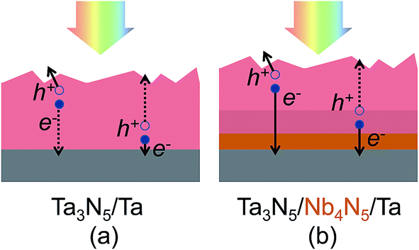 | ||
| Fig. 9 Schematic depicting the separation and transport of photogenerated electrons and holes in (a) Ta3N5/Ta and (b) Ta3N5/NbNx/Ta films. | ||
A photoanode configuration consisting of a lower oriented Ta3N5 layer and an upper disordered Ta3N5 layer represents a combination of a short migration distance for photoexcited holes and efficient electron transport toward the back conductor layer. The introduction of the NbNx interlayer effectively realizes this ideal photoanode configuration and thus enhances the PEC performance. This result suggests that the structural and PEC properties of Ta3N5 photoanodes can be improved by designing appropriate interlayers, regardless of the nitridation of the Ta3N5 film and the particular back conductor material employed. The film transfer method developed in this study presents a means of studying such aspects owing to the controllability of the thickness and the stacking order of multilayers.
Conclusions
NbNx layers principally consisting of Nb4N5 were introduced as interlayers between Ta3N5 films and the back substrate, using the film transfer method. The Nb4N5 interlayer did not change the phase purities and the crystallite sizes of the Ta3N5 films significantly, although the preference in the crystalline orientation of the Ta3N5 film was enhanced by the Nb4N5 phase. The photocurrents obtained from Ta3N5 photoanodes during the PEC water oxidation reaction increased significantly in the presence of the NbNx interlayer. The results of zone-axis imaging and electron diffraction from cross-sectional TEM revealed that ordered growth of the Ta3N5 film occurred and that a 200 nm layer of highly grain-oriented Ta3N5 was formed near the Ta3N5/NbNx interface. The formation of an oriented Ta3N5 layer did not affect the ECSA, flat band potential or carrier density of a 630 nm Ta3N5 film. The increased photocurrent associated with the presence of a NbNx interlayer is primarily attributed to the increased long distance electron mobility in the Ta3N5 film. The film growth on the Nb4N5 layer observed in this work demonstrates the key roles of a buffer layer in the design and synthesis of efficient Ta3N5 photoelectrodes.Acknowledgements
This work was financially supported by Grants-in-Aid for Specially Promoted Research (No. 23000009) and for Young Scientists (A) (No. 15H05494) and Young Scientists (B) (No. 5K17895) of Japan Society for the Promotion of Science (JSPS). This work was partly supported by the Artificial Photosynthesis Project of the New Energy and Industrial Technology Development Organization (NEDO) and Companhia Brasileira de Metalurgia e Mineração (CBMM). Part of this work was conducted at the Research Hub for Advanced Nano Characterization at the University of Tokyo, under the support of the “Nanotechnology Platform” (project No. 12024046) of the Ministry of Education, Culture, Sports, Science and Technology (MEXT), Japan. The authors thank Dr Qian Wang, Dr Miao Zhong, Dr Taro Yamada and Mr Yutaka Sasaki of the University of Tokyo for SEM characterisation and discussion.References
- A. J. Nozik, Annu. Rev. Phys. Chem., 1978, 29, 189–222 CrossRef CAS.
- M. Grätzel, Nature, 2001, 414, 338–344 CrossRef PubMed.
- A. Fujishima and K. Honda, Nature, 1972, 238, 37–38 CrossRef CAS PubMed.
- W. J. Chun, A. Ishikawa, H. Fujisawa, T. Takata, J. N. Kondo, M. Hara, M. Kawai, Y. Matsumoto and K. Domen, J. Phys. Chem. B, 2003, 107, 1798–1803 CrossRef CAS.
- T. W. Kim and K.-S. Choi, Science, 2014, 343, 990–994 CrossRef CAS PubMed.
- Y. Li, T. Takata, D. Cha, K. Takanabe, T. Minegishi, J. Kubota and K. Domen, Adv. Mater., 2013, 25, 125–131 CrossRef CAS PubMed.
- M. Zhong, Y. Ma, P. Oleynikov, K. Domen and J.-J. Delaunay, Energy Environ. Sci., 2014, 7, 1693–1699 CAS.
- H. X. Dang, N. T. Hahn, H. S. Park, A. J. Bard and C. B. Mullins, J. Phys. Chem. C, 2012, 116, 19225–19232 CAS.
- T. Minegishi, N. Nishimura, J. Kubota and K. Domen, Chem. Sci., 2013, 4, 1120–1124 RSC.
- K. Ueda, T. Minegishi, J. Clune, M. Nakabayashi, T. Hisatomi, H. Nishiyama, M. Katayama, N. Shibata, J. Kubota, T. Yamada and K. Domen, J. Am. Chem. Soc., 2015, 137, 2227–2230 CrossRef CAS PubMed.
- Y. Li, L. Zhang, A. Torres-Pardo, J. M. Gonzalez-Calbet, Y. Ma, P. Oleynikov, O. Terasaki, S. Asahina, M. Shima, D. Cha, L. Zhao, K. Takanabe, J. Kubota and K. Domen, Nat. Commun., 2013, 4, 2566 Search PubMed.
- S. Hu, M. R. Shaner, J. A. Beardslee, M. Lichterman, B. S. Brunschwig and N. S. Lewis, Science, 2014, 344, 1005–1009 CrossRef CAS PubMed.
- L. Chen, J. Yang, S. Klaus, L. J. Lee, R. Woods-Robinson, J. Ma, Y. Lum, J. K. Cooper, F. M. Toma, L. W. Wang, I. D. Sharp, A. T. Bell and J. W. Ager, J. Am. Chem. Soc., 2015, 137, 9595–9603 CrossRef CAS PubMed.
- G. Liu, J. Shi, F. Zhang, Z. Chen, J. Han, C. Ding, S. Chen, Z. Wang, H. Han and C. Li, Angew. Chem., Int. Ed., 2014, 53, 7295–7299 CrossRef CAS PubMed.
- G. Liu, P. Fu, L. Zhou, P. Yan, C. Ding, J. Shi and C. Li, Chem.–Eur. J., 2015, 21, 9624–9628 CrossRef CAS PubMed.
- J. Seo, T. Takata, M. Nakabayashi, T. Hisatomi, N. Shibata, T. Minegishi and K. Domen, J. Am. Chem. Soc., 2015, 137, 12780–12783 CrossRef CAS PubMed.
- J. M. Morbec, I. Narkeviciute, T. F. Jaramillo and G. Galli, Phys. Rev. B, 2014, 90, 155204 CrossRef.
- B. A. Pinaud, P. C. K. Vesborg and T. F. Jaramillo, J. Phys. Chem. C, 2012, 116, 15918–15924 CAS.
- M. X. Li, W. J. Luo, D. P. Cao, X. Zhao, Z. S. Li, T. Yu and Z. G. Zou, Angew. Chem., Int. Ed., 2013, 52, 11016–11020 CrossRef CAS PubMed.
- B. A. Pinaud, A. Vailionis and T. F. Jaramillo, Chem. Mater., 2014, 26, 1576–1582 CrossRef CAS.
- S. Nakamura, Jpn. J. Appl. Phys., 1991, 30, 1705–1707 CrossRef CAS.
- F. A. Ponce and D. P. Bour, Nature, 1997, 386, 351–359 CrossRef CAS.
- A. Dabirian and R. van de Krol, Chem. Mater., 2015, 27, 708–715 CrossRef CAS.
- G. Liu, S. Ye, P. Yan, F. Xiong, P. Fu, Z. Wang, Z. Chen, J. Shi and C. Li, Energy Environ. Sci., 2016, 9, 1327–1334 CAS.
- C. Wang, T. Hisatomi, T. Minegishi, M. Nakabayashi, N. Shibata, M. Katayama and K. Domen, Chem. Sci., 2016, 7, 5821–5826 RSC.
- C. C. L. McCrory, S. Jung, J. C. Peters and T. F. Jaramillo, J. Am. Chem. Soc., 2013, 135, 16977–16987 CrossRef CAS PubMed.
- R. Fix, R. G. Gordon and D. M. Hoffman, Chem. Mater., 1993, 5, 614–619 CrossRef CAS.
- T. Nobuzo, Jpn. J. Appl. Phys., 1971, 10, 248–259 CrossRef.
- G. Oya and Y. Onodera, J. Appl. Phys., 1974, 45, 1389–1397 CrossRef CAS.
- G. M. Carroll, D. K. Zhong and D. R. Gamelin, Energy Environ. Sci., 2015, 8, 577–584 CAS.
- S. Chen and L.-W. Wang, Chem. Mater., 2012, 24, 3659–3666 CrossRef CAS.
- A. H. Reshak, Comput. Mater. Sci., 2014, 89, 45–51 CrossRef CAS.
- B. Klahr, S. Gimenez, F. Fabregat-Santiago, J. Bisquert and T. W. Hamann, Energy Environ. Sci., 2012, 5, 7626–7636 CAS.
Footnote |
| † Electronic supplementary information (ESI) available. See DOI: 10.1039/c6ta04363a |
| This journal is © The Royal Society of Chemistry 2016 |