
 Open Access Article
 This Open Access Article is licensed under a
 Creative Commons Attribution 3.0 Unported Licence
Chemical vapor deposition grown formamidinium perovskite solar modules with high steady state power and thermal stability†
Matthew R.
Leyden
,
Yan
Jiang
and
Yabing
Qi
*
Energy Materials and Surface Sciences Unit (EMSS), Okinawa Institute of Science and Technology Graduate University (OIST), 1919-1 Tancha Onna-son, Okinawa 904-0495, Japan. E-mail: Yabing.Qi@OIST.jp
First published on 8th July 2016
Abstract
Metal organic halide perovskites are promising materials for solar cells with a maximum certified efficiency of 22.1%. However, there are only a handful of reports on larger area modules, where efficiencies drop with increasing use of the active area. Chemical vapor deposition (CVD) is a technology used in many industrial applications demonstrating potential for scale up. We used a CVD process to fabricate MAPbI3 and FAPbI3 based solar cells with power conversion efficiencies (PCEs) up to 15.6% (MAI, 0.09 cm2) and 5 × 5 cm modules with 9.5% (FAI, 5-cell modules, total active area 8.8 cm2) and 9.0% (FAI, 6-cell modules, total active area 12 cm2). To further investigate scaling issues, we fabricated modules using an established MAPbI3 solution process, and demonstrated maximum PCEs of 18.3% (MAI, 0.1 cm2), 14.6% (MAI, 1 cm2 single cells), and 8.5% at 5 × 5 cm (MAI, 6-cell module, total active area 15.4 cm2). The solution processed cells performed better than CVD cells when comparing PCEs determined from J–V measurements, but the steady state power of solution processed solar cells decreased quickly with increasing area. This decrease in power was correlated with rapid heating of the solar cells under 1 sun illumination, with a pronounced drop in performance at the phase transition temperature of MAPbI3. In contrast, FAPbI3 CVD grown solar modules maintained much of their PCEs transitioning from J–V measurements to the steady state operating conditions (1 sun), suggesting that the FAI based CVD process may outperform MAI based solution processed modules when scaled up to practical sizes.
Introduction
Perovskite solar cells have demonstrated impressive efficiencies up to 22.1%,1 but the efficiencies of devices over 1 cm2 in size are typically significantly lower. There are several reports demonstrating 1 cm2 sized solar cells with efficiencies between 15 and 20%.2–4 When the size is increased further, fabricating a multi-cell module becomes necessary to raise the output voltage to practical values, and to circumvent the series resistance issue of the transparent conductive contact. The demonstrated efficiencies of modules are typically significantly lower than those of the 1 cm2 single cells, but there are a few exceptional studies reporting high efficiencies even with a large area. Heo and co-workers reported a 12.9% module with an active area of 40 cm2.5 This work is excellent, but when the total substrate area (i.e. the area of the substrate on which the solar module was fabricated) is considered the effective efficiency drops to 5.2%. This concept will be referred to as PCE per total area, which is in contrast to PCE per active area. This is typical of published perovskite solar cells and modules (Fig. S1†), i.e. in general PCEs drop with increasing active area and with increasing use of the total substrate area.6–11 Qiu et al. addressed the point of area use and demonstrated a module with 91% of the total area being active, while maintaining a 13.6% PCE with a total aperture area of 4 cm2.12 This high use of the area was accomplished by mechanically scribing narrow features for module patterning. Also, in this work the total area was defined with an aperture, not the substrate size. Because the total substrate area was not mentioned in this work, it is not possible to determine PCE per total substrate area of their solar modules. This concept will be referred to as PCE per aperture area (i.e. with the edge area excluded), which is essentially an upper-bound of PCE per total area. Other studies have demonstrated 84% use of the area with laser scribing, and demonstrated 5.5% PCE per aperture area.13 A direct comparison of PCEs between reported modules comparing PCE per active area, PCE per aperture area, and PCE per total area may not be completely fair, as authors likely design their module with a particular measurement in mind, so a summary of reported PCE per active area (Fig. S1a†), and PCE per total area (Fig. S1b†) and PCE per aperture area (Fig. S1c†) is provided in the ESI.† But it is important to keep in mind that PCE per total area is more relevant for practical applications than PCE per active area, as the unused area also needs to be installed. Resolving the issues of a low active area may require non-trivial modification to an otherwise successful protocol, and using a high active area can introduce new issues such as substrate heating or poor shunt resistance as discussed in the latter part of this work.Chemical vapor deposition (CVD) is a process widely used in industry, and is one of the many ways demonstrated for vapor deposition of perovskites.14 Vapor deposited perovskites can be formed under high15–18 and low vacuum conditions. In this work CVD is categorized as a non-directional, low to atmospheric pressure process. There are a number of studies using CVD to fabricate perovskite solar cells, such as low vacuum single step processing,19 sequential deposition processing,20–25 and growth under atmospheric conditions.26 Perovskite modules grown by CVD have already been demonstrated with a PCE per active area of 6.2%, with an active area of 8.4 cm2.8 CVD offers potential for batch processing for higher throughput, low fabrication cost, flat uniform perovskite films over large areas, and semi-transparent solar cells.20,22 In this work we investigated the scalability of the CVD process by fabricating both single solar cells with different sizes and solar modules. We also compared these cells and modules to solution processed counterparts. Using CVD we demonstrated a small area methyl ammonium iodide (MAI) based champion cell with a PCE of 15.6% (active area = 0.09 cm2), which is the highest reported efficiency for CVD based perovskite solar cells. In addition we made formamidinium iodide (FAI) based modules on 5 × 5 cm substrates with champion PCEs per active area of 9.5% and 9.0% with active areas of 8.8 cm2 and 12 cm2, respectively. These solar modules are used as the primary reference points in this work. CVD processed modules were made with a larger active area of 15.4 cm2 and demonstrated a PCE per active area of 5.8%, but were not used as the reference points for this work. The TiO2 layer of these modules was patterned incorrectly, creating electrical shorting pathways between cells within the module that should be electrically isolated. This issue significantly limited solar module performance and complicated the comparison to other modules (discussed further in the Experimental section).
Results and discussion
We chose a formamidinium based perovskite layer (i.e., FAPbI3) to fabricate large cells and modules because of the higher temperature stability of resultant perovskite films.25 This process used physical vapor deposition of lead halide, where lead halide was patterned with a shadow mask. During the CVD growth process, the perovskite is selectively grown only on the area pre-deposited with lead halide. The selective growth of the perovskite layer simplifies module fabrication as the perovskite layer does not need to be etched/scribed away after growth. Photographs of completed modules grown by CVD are shown in Fig. 1, and specific dimensions are provided in Fig. S2.† The process of perovskite film growth and solar cell fabrication is similar to previous reports, except for a few minor variations discussed in the experimental section. To have a relevant reference point we fabricated solar cells using the Lewis base adduct method, which has been reported to produce high performance cells.27 Similar to many other perovskite fabrication methods, perovskite solar cells grown by the CVD process and our reference solution process suffer from reduced PCEs when scaling to higher active areas. A summary of performance measured by current–voltage (J–V) curves as a function of the active area is shown in Table 1.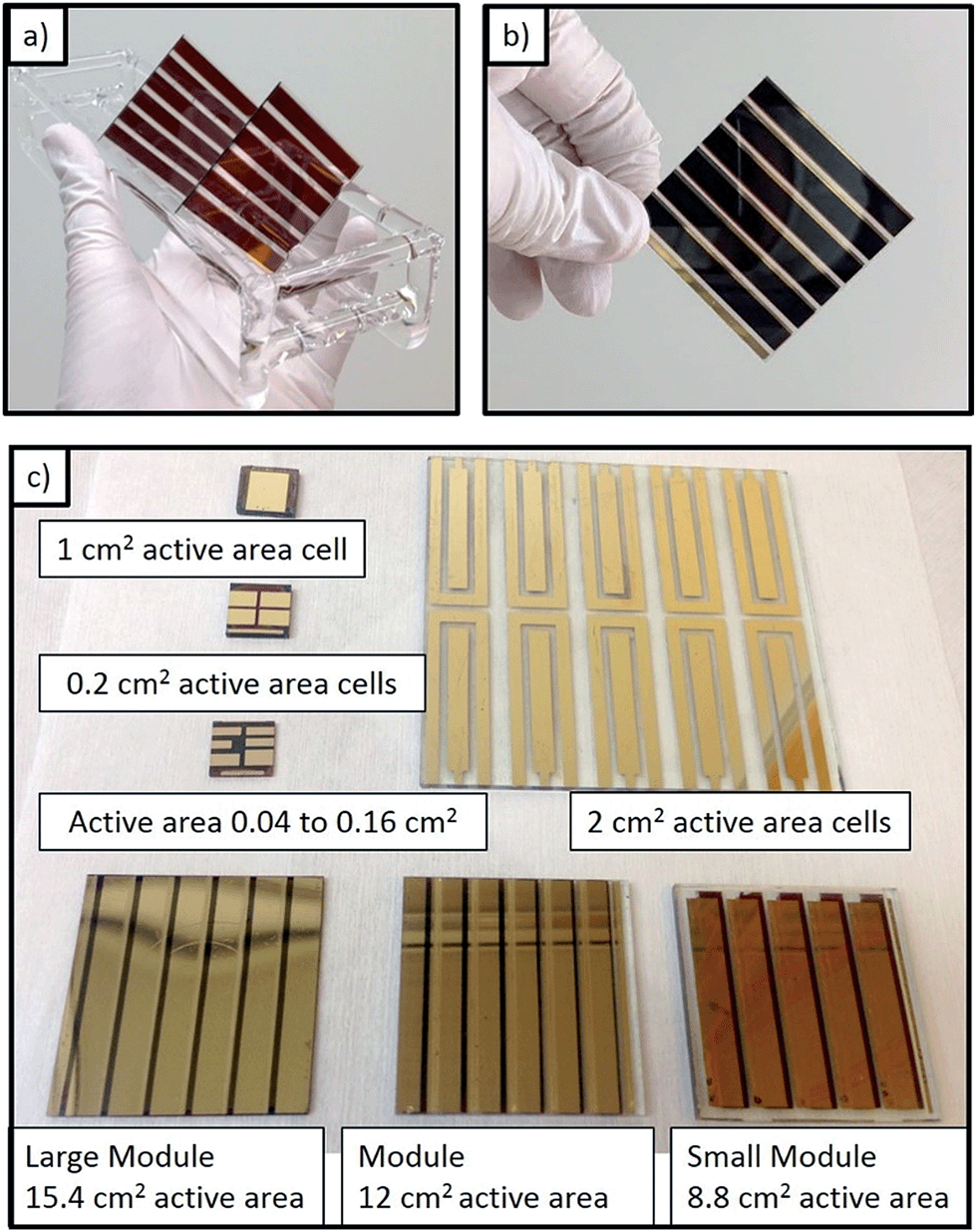 | ||
| Fig. 1 (a) Photograph of patterned perovskite films grown by CVD. (b) Complete perovskite solar cell module grown by the CVD process, shown from the rear side. (c) Photographs of cells and modules presented in this work. | ||
| Cells and modules | Cell size (cm2) | Normalized Voc | Normalized Jsc (mA cm−2) | Fill factor | Efficiency% (steady state) |
|---|---|---|---|---|---|
| Champion CVD cell (MAI) | 0.09 | 1.06 | 21.7 | 68 | 15.6 |
| Champion solution cell (MAI) | 0.10 | 1.07 | 22.4 | 76 | 18.3 |
| Champion solution cell (MAI) | 1.0 | 1.12 | 20.5 | 68 | 14.6 (13.7) |
| Champion CVD cell (FAI) | 2.0 | 1.02 | 19.5 | 53 | 10.4 |
| Average CVD cell (FAI, spiro) | 2 | 0.97 ± 0.05 | 17.1 ± 1.3 | 47 ± 6 | 7.8 ± 1.3 |
| Average CVD cell (FAI, P3HT) | 2 | 0.93 ± 0.03 | 20.3 ± 1.1 | 41 ± 3 | 7.8 ± 0.9 |
| Champion CVD module (FAI) | 8.8 | 0.98 | 16.9 | 57 | 9.5 (7.6) |
| Champion CVD module (FAI) | 12.0 | 0.94 | 17.8 | 54 | 9.0 (8.8) |
| Champ. solution module (MAI) | 12.0 | 0.84 | 19.9 | 43 | 7.1 (7.0) |
| Champ. solution module (MAI) | 15.4 | 0.98 | 19.0 | 46 | 8.5 (4.0) |
| CVD module (FAI) | 15.4 | 0.77 | 15.2 | 49 | 5.8 |
When scaling to larger areas, the most pronounced drop in performance resulted from the reduction in fill factor and short circuit current (Jsc). The open circuit voltage (Voc) also decreases slightly as the area is increased, but not as significantly as the fill factor and Jsc. The decrease in the fill factor can be explained by an increase in series resistance due to a longer transport distance through fluorine doped tin oxide (FTO), or poor contact between cells. This is an important issue, and can be solved with optimized module fabrication and design. For example, fabricating narrower cells reduces the travel distance through the FTO, and therefore lowers series resistance. The decrease in Jsc is more intrinsic to the perovskite growth process and likely reflects the average performance. Indeed, we see that the average Jsc for the champion modules (16.9 mA cm−2 and 17.8 mA cm−2) is closer to the average of 2 cm2 cells (17.1 mA cm−2) than to the champion 2 cm2 cell (19.5 mA cm−2). We also demonstrated that poly(3-hexylthiophene-2,5-diyl) (P3HT) can be used successfully as a hole transport layer for large area cells with comparable efficiency.
The results in Table 1 suggest that the solution processed cells have higher nominal PCEs (determined from conventional J–V measurements) when comparing similar area devices. However, this trend changed after switching from conventional J–V measurements to steady state operating conditions at the maximum power point. The steady state power is lower than the peak power reported by J–V curves for both CVD and solution methods, but the difference is more pronounced in the solution processed modules.
A previous report demonstrated an FAI based cell prepared by CVD with an active area of 0.04 cm2 to have a nominal PCE of 14.2% and a steady state power of 11.3%.25 This difference between power measured by J–V curves and power measured at the steady state can become increasingly significant as areas become larger. To illustrate such an area dependence, we compared the champion CVD grown solar modules to a solution processed single solar cell and then to a solution processed solar module with a larger active area (Fig. 2). The solution processed champion cell had an active area of 1 cm2 and a nominal PCE of 14.6%. The steady state PCE of this cell was 13.7% and maintained much of its PCE after many hours (approximately 38 h) of operation (Fig. S3†). The peak steady state PCE of the 12 cm2 active area CVD module was 8.8% measured after 30 h of operation. This 40 h steady state measurement was periodically interrupted to measure J–V curves and redefine the maximum power point (Fig. 2b). In contrast to the solution processed cells or CVD modules the steady state power of the solution processed modules slowly decreased with time (Fig. 2a). From this figure we can see that the solution module achieved a peak power of ∼7.9%, but decayed to 7% after 3 hours of continuous operation (6.5%, after 8 h). Both 12 cm2 modules are possibly limited to about ∼9% by series resistance (discussed in the ESI†). The PCE decay for solution processed modules was even more rapid for cells with high use of active area, possible reasons for which are discussed below.
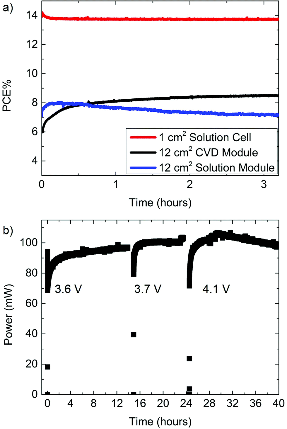 | ||
| Fig. 2 Steady state power tracking for solution prepared and CVD grown cells and modules. (a) Steady state power per unit active area of the champion solution processed cell (at 0.86 V, PCE by J–V = 14.6%, 1 cm2), solution processed module (at 3.7 V, PCE by J–V = 7.1%, 12 cm2), and champion CVD grown module (at 4.1 V, PCE by J–V = 9.0%, 12 cm2). (b) Long term steady state measurement of the 12 cm2 CVD module which reached a maximum steady state power of 106 mW (8.8%, at 4.1 V) after ∼30 hours of operation. | ||
A larger active area module using a 5 × 5 cm substrate and an active area of 15.4 cm2 was made by the Lewis base adduct solution method and had a nominal PCE of 8.5% (nominal power = 131 mW), but a steady state PCE of only 4% (steady state power = 62 mW). This cell was the best of 9 modules using the same process. This module compared poorly to the lower active area champion CVD grown modules with steady state power 66 mW (8.8 cm2 steady state PCE = 7.6%) and 106 mW (12 cm2 steady state PCE = 8.8%), as shown in Fig. 2b. One possible cause for this drop in efficiency is related to substrate heating, which is discussed later. The decrease could also be related to difficulties in applying the Lewis base adduct solution method on larger substrates. The champion solution processed 1 cm2 sample has the same substrate size (15 mm × 15 mm; see Fig. 1c and S2† for specific dimensions) and deposition conditions as the highest performing cell in this work (18.3% PCE, 0.1 cm2). This is mentioned to highlight processing differences between small cells (active area ≤ 1 cm2) and larger modules.
This lower total power despite having a larger active area was surprising, and raised concerns that perhaps substrate heating was limiting the performance.28 The MAI based perovskite will undergo a phase transition at elevated temperatures (54–57 °C) from the tetragonal to the cubic phase,29,30 and this phase transition is believed to cause reduced performance.28 We observed that the solution processed cell heated up to 54 °C within a few minutes of testing under 1 sun illumination and rapidly dropped in PCE, but would regain efficiency when removed from the solar simulator and allowed to cool. However, this behaviour is not completely due to the phase transition of the perovskite film (Fig. S4†). Decay in performance is observed from heating at temperatures below the transition temperature as well, and loss in performance cannot be exclusively explained by the transition. It is possible that heating accelerates a decay process that is significant in solution processed large-area modules, but less significant in small-area cells. Shunt pathways are reported to cause degradation,31 and the use of large modules provides more possible pathways than smaller substrates.
To demonstrate more clearly the impact of the phase transition, the intensity of the solar simulator was increased to 1.5 sun, allowing the module to rapidly heat beyond the transition temperature (Fig. 3a). The temperature was monitored in situ by using a thermocouple placed on the underside at the center of the module. A phase transition was indeed observed at ∼52 °C by a latent heating rate and an increase in the decay rate of the steady state current. Note that there may be a lag between the temperature of the thermocouple and that of the perovskite film, explaining the lower than expected transition temperature. Operating in the cubic phase not only caused a rapid decay in performance, but also appeared to increase the dark current, evident from the large negative power when the light was turned off. A similar increase in the dark current was also observed when operating at 1 sun intensity (Fig. S4†). The dark current partially recovered to a lower value if the cell was allowed to cool and given sufficient time before the next measurement. Based on this observation it is possible that the perovskite slowly returns to the tetragonal phase, allowing the cell to partially recover performance. This residual material in the cubic phase may explain why the second phase transition in Fig. 3a is less distinct.
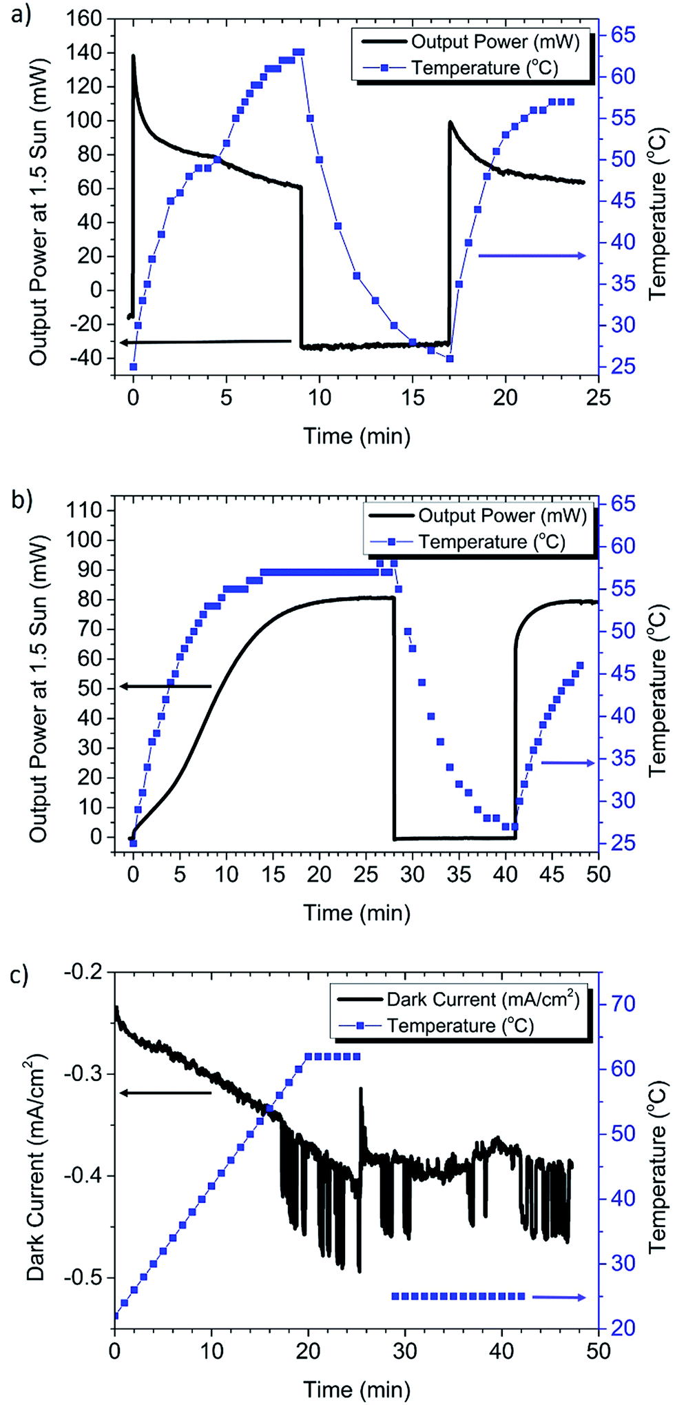 | ||
| Fig. 3 Temperature and current monitoring of modules. These graphs indicate that the phase transition of MAPbI3 is likely impacting the performance during steady state operation, and highlights that FAI does not have a phase transition in this temperature range. (a) Measurement of the champion MAPbI3 solution processed module at 1.5 sun. This shows a phase transition at around ∼52 °C to the cubic phase, with a corresponding rapid drop in the steady state power. Subsequently there was an increase in the dark current, observed here by a high negative power. (b) FAPbI3 CVD grown module, which was not observed to be significantly impacted by substrate heating at 1.5 sun. This figure also shows a light soaking dependence characteristic of CVD grown cells. (c) Dark current measurements as a function of temperature on the MAPbI3 module show an increase in current with increasing temperature and increased noise at the phase transition temperature (∼57 °C). | ||
When the FAI based CVD grown perovskite solar module was measured at 1.5 sun (Fig. 3b), there was no evidence of performance decay with increasing temperature. This is reasonable, because there is no phase transition for FAPbI3 in the temperature range of solar cell operation. However, the FAI based CVD grown perovskite solar module had a pronounced dependence on light soaking, which is discussed in more detail below. These comparative results suggest that the CVD growth of the FAI based perovskite maintains a better steady state PCE going from small to large areas than the MAI based Lewis base adduct solution method. It is possible that the solution process may require further optimization for large scale substrates, such as improving the module patterning process to reduce the opportunities for shunt pathways, modification of anti-solvent deposition conditions, or use of FAI instead of MAI.32
To decouple the effects of temperature from possible light induced effects, an additional control experiment was performed on the MAPbI3 solution processed module by recording dark current during heating of the module on a hotplate (Fig. 3c). Here the hotplate was ramped up to 62 °C at a constant rate of 2°C min−1, at the approximate maximum power point (3.9 V). In this figure we can see that the dark current increases with increasing temperature, with a sharp increase in the current and noise at the phase transition temperature (∼57 °C). After 5 min at 62 °C the module is removed from the hotplate and allowed to cool to room temperature, and the dark current remains at a high level, which is similar to that in Fig. 3a. We see from Fig. 3c that the dark current stops rising once the cell is removed from heat. This suggests that the increasing dark current is not due to voltage induced ion migration alone. However ion migration could be accelerated by heating, or by the transition to the cubic phase.
In Fig. 4a cells from the 8.8 cm2 champion CVD module are added in series one at a time to show the additive nature in Voc. To our surprise, the weak performing Jsc of cell #1 (15.9 mA cm−2) did not seem to rigidly limit the Jsc of the entire module (16.9 mA cm−2). This observation led us to consider whether possibly perovskite modules are tolerant to partial shade, similar to reports on electrolyte based dye sensitized solar cells. Dye sensitized solar cells can be modelled as a two-diode system, where the Jsc of a module may be minimally impacted by a weak performer.33 To test this hypothesis, a second perovskite module was used and 3 of its 5 cells were covered with semitransparent tape. Fig. 4b shows the cells, uncovered and with 1 layer and 2 layers of tape. Both Jsc and Voc are strongly impacted by the shadowing of cells in a module. From these partial shade experiments it is clear that perovskite modules are not especially tolerant to partial shade, and behave more like silicon solar cells,34 than dye sensitized solar cells. This means that perovskite modules should have bypass diodes, allowing them to pass current through a cell with a lower photocurrent, and subsequently tolerate partial shade. An alternative explanation of the behavior seen in Fig. 4a can be given by a combination of a low shunt resistance and low recombination resistance of the weak performing cell 1. A low shunt resistance can pass the excess current supplied by the higher performing cells.
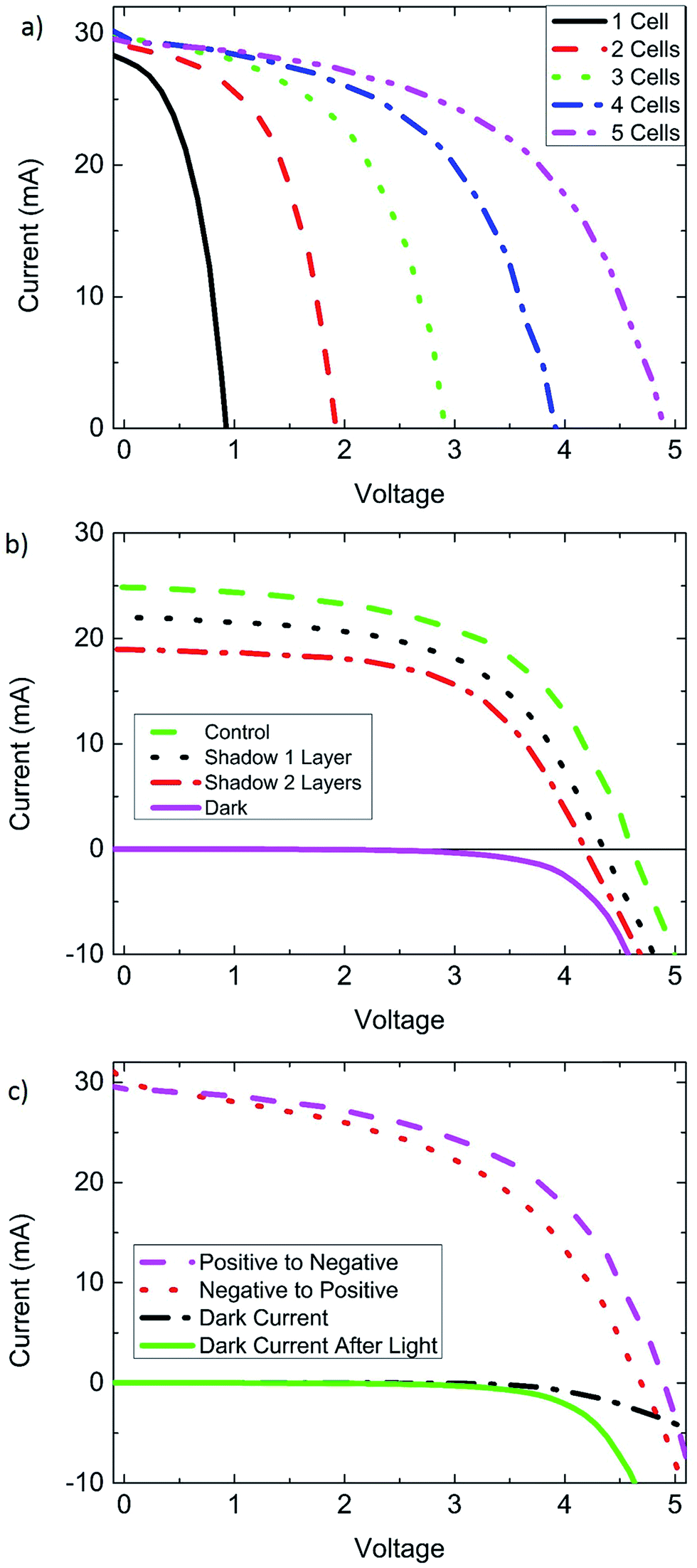 | ||
| Fig. 4 The behavior of perovskite solar cell modules grown by chemical vapor deposition, and their response to partial shade or light soaking. (a) Champion CVD module (8.8 cm2) J–V curves, where cells from the module are added in series, demonstrating the addition of Voc. Cell 1 was a comparatively weak performer, however the Jsc of the entire module was not strongly limited by the Jsc of cell 1. (b) Curves from a second module demonstrating its response to partial shade, where the performance decreases similar to silicon solar cells. (c) Forward and reverse scans of the champion CVD module and dark current measurements. The second dark measurement was taken after light soaking for 1 h. This demonstrates the impact of light soaking, and its role even when the light is off. | ||
Perovskite solar cells grown by CVD exhibit a pronounced sensitivity and improved performance from light soaking similar to many other reports on perovskite solar cells. This can be explained by light induced self-poling of the perovskite layer, causing migration of ions within the perovskite film.35 Light induced poling appears to be present in the solution processed MAI cells as well as FAI based CVD processed cells, but the time scale of solution processed cells seems much shorter. Differences could be due to the speed of ion migration in the material (FAPbI3vs. MAPbI3), and how far the ions migrate, and the structure of the film. Other possible explanations for this behavior include UV illumination creating photoactive surface states, or shifting of the conduction band edge in TiO2.36 The effects of light soaking are more noticeable as the area is increased. Small cells often reached full efficiency after minutes of light soaking, while larger cells could take up to an hour or more before reaching a stable efficiency. Light soaking impacted dark current measurements, indicating that the effect of light soaking is long lasting and is present even after the light is turned off (Fig. 3b and 4c).
Fig. 5 shows J–V curves from champion small area cells for both CVD and solution processing, in addition to EQE curves showing approximate agreement between the integrated current and Jsc measured from J–V curves. However, as shown in the previous figures, J–V curves only offer an indication of how a cell may perform during steady state conditions. Also, larger area modules may behave differently from their small area counterparts.
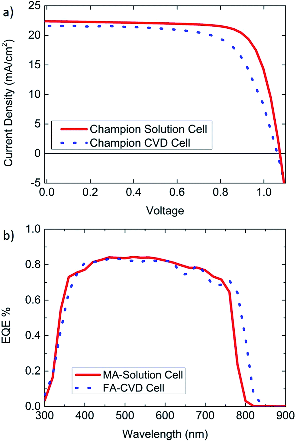 | ||
| Fig. 5 Champion small area solar cells (a) the champion solution processed cell was measured to have a PCE of 18.3% (0.1 cm2) and a Jsc of 22.4 mA cm−2, while the champion MAI based CVD cell has a PCE of 15.6% (0.09 cm2) and a Jsc of 21.6 mA cm−2. (b) External quantum efficiency (EQE) spectra from CVD and solution processed cells. The FAI based CVD cell has an integrated current of 21.1 mA cm−2 and an absorption edge at a slightly longer wavelength than the EQE from the MAI based solution processed cell with an integrated current of 20.3 mA cm−2. | ||
Experimental
TiO2 deposition and patterning
For small CVD grown modules, FTO glass (8 Ω □−1, Sigma Aldrich) was patterned by photolithography and dry etched using 30 min of inductively coupled plasma (ICP, Oxford Instruments, 100 w RF, 200 w ICP, 10 sccm CF4, 40 sccm H2, 10 sccm CH4, at a pressure of 40 mTorr). The photoresist was removed by sonicating substrates in acetone followed by UV ozone treatment. For larger active area modules the FTO was purchased pre-patterned (FTO glass, Yingkou OPV-tech New Energy). For CVD grown modules, a compact layer of TiO2 was deposited by spray pyrolysis using a solution of 75 wt% titanium diisopropoxide bis(acetylacetonate) in isopropanol (Sigma Aldrich) on a pre-heated hot plate at 480 °C. This layer was approximately 100 nm thick. This process formed a uniform compact layer over the entire surface. This is generally desirable, but was found to be conductive enough to short adjacent cells in the large module geometry. The spacing between FTO cells in the large modules was relatively small (200 μm), allowing for high conductivity between cells after TiO2 deposition (300 ± 90 ohms).These titanium oxide layers were then patterned by photolithography and etched with a timed dry etch ICP process (Oxford instruments, 6 min, 100 w RF, 200 w ICP, 16 sccm CF4, 4 sccm Ar, at a pressure of 40 mTorr), largely removing the TiO2, while leaving a continuous layer of underlying FTO. The photoresist is then removed by using boiling acetone, followed by UV-ozone treatment. A photograph of the resulting film can be seen in the ESI (Fig. S5†). This etching process was sufficient to eliminate the contact between cells caused by compact layer TiO2 in the small modules, but for large modules with narrow spacing between cells there remained conductive paths (100 ± 80 kohm). At the time of fabrication, this was thought to be sufficient insulation, but this conductivity appeared to limit the Voc obtained in CVD grown perovskite large modules. This problem was addressed by increasing the spacing between FTO cells to 1 mm (12 cm2 active area). With increasing spacing it is possible to pattern TiO2 deposition with a shadow mask (Fig. S5†), eliminating the need for photolithography and plasma processing.
To fabricate the mesoporous layer for solution processed cells and modules 0.15 M titanium diisopropoxide dis(acetylacetonate) (Sigma Aldrich) in butanol was spun onto substrates at 2800 rpm and dried at ∼120 °C, followed by a 0.1 g mL−1 solution of titanium dioxide nanoparticles in butanol at 2000 rpm. The film is then annealed at 550 °C. These substrates were then treated with 20 mM TiCl4 in DI water for 10 min at 70 °C, followed by a second anneal at 500 °C. These titanium oxide layers were then patterned by photolithography and etched with a timed ICP process, in the same way as performed for compact TIO2 by spray pyrolysis. No conductive path was observed between cells in the large modules after patterning with the ICP, suggesting that the TiO2 formed by solution deposition is less dense and continuous than by spray pyrolysis. This could also be related to dark current measurements and the formation of shunt pathways, which show more dark current than cells made by spray pyrolysis (Fig. 3 and S6†). For this reason, the compact layer of the 12 cm2 active area solution module was made by spray pyrolysis.
Perovskite growth by CVD
Perovskite films were grown in a two-step process where lead halide was first deposited onto TiO2/FTO substrates, followed by CVD deposition of MAI or FAI (Dyesol) which converted films to perovskites. Perovskite films were prepared by depositing an ∼180 nm layer of lead iodide or 120 nm of lead chloride onto substrates by thermal evaporation (at ∼1 × 10⁻³ Pa, ∼0.5 Å s−1, using the PbCl2/PbI2 powder, Sigma-Aldrich). Each material was deposited separately, and not on the same cell, and both can be used with comparable results. The thickness was monitored with a quartz-crystal microbalance and additionally measured using a profilometer. Lead halide coated substrates were loaded into a 2-zone CVD furnace (130 mm O.D. quartz tube). The first zone was loaded with ∼1 g of solid FAI powder and the second zone with substrates. The CVD was pumped down to a pressure of ∼100 Pa, with a flow of dry nitrogen. Substrates were heated to 160 °C, followed by heating the zone with MAI or FAI powder to 210 °C. In order to obtain similar conversion rates to previous reports the maximum temperature was increased from 180 to 210 °C. The total deposition time is approximately 45 min, including 30 min for the powder to cool below its sublimation temperature. After the source zone is cooled, the substrates were allowed to cool, the CVD was vented, and substrates were removed. The amount of sublimated powder was not sensitive to the mass loaded, but depended more on temperature and time. For example, growth runs loaded with 0.6 g, 1.2 g, and 1.8 grams of FAI all consumed ∼160 mg of the FAI powder.Solution processed perovskite
We prepared the following solution as a perovskite precursor: PbI2 466 mg (TCI Chemicals), methyl ammonium iodide 159 mg, dimethylformamide 530 μL, and dimethyl sulfoxide 73 μL. This solution is spun onto mesoporous TiO2 substrates at 4000 rpm for 30 s. During spin coating diethyl ether is added as an anti-solvent at ∼9 s, with a volume of 0.2 mL for 1.5 × 1.5 cm substrates and 1 mL for 5 × 5 cm substrates. The resultant films were annealed on a hotplate for 1 h at 100 °C.Device fabrication
Solar cells were fabricated by spin-coating a hole transport layer containing three materials: spiro-MeOTAD (2,2′,7,7′-tetrakis(N,N-di-p-methoxy-phenylamine)-9,9′-spirobifluorene) (Suna Tech Inc for CVD perovskite, and Merck for solution processed cells) dissolved in chlorobenzene (70 mg mL−1), 20 μL of Li-bis (trifluoromethanesulfonyl)-imide (LiTFSI, Sigma) dissolved in acetonitrile (500 mg mL−1), and 30 μL of tert-butylpyridine (t-BP, Sigma). Top electrodes were 80 nm of gold, deposited by thermal evaporation (∼1.0 × 10⁻⁶ Torr, at 0.1–0.3 Å s−1) through a shadow mask. Specific dimensions of the module are provided in Fig. S2† and photos of the shadow mask are provided in Fig. S5.†Solar cell measurements
Current–voltage (J–V) characteristics of small area solar cells were measured under 1 sun illumination (AM 1.5 G, 100 mW cm−2, calibrated with a Newport reference cell) using a solar simulator (Newport Oriel Sol 1A) and a Keithley 2400 source meter in ambient air at ∼25 °C and a relative humidity of ∼40–50%. The solution processed cells were measured using a 0.1 cm2 anodized aluminium mask. The champion small area CVD was fabricated prior to our implementation of masking, and was not masked. All large area cells and modules were measured under 1 sun illumination (AM 1.5 G, 100 mW cm−2, calibrated with a Newport reference cell) using a PEC_L01 portable solar simulator inside of a low humidity glove box (<10% RH). All J–V measurements for individual cells are measured at a scan rate of 0.35 V s−1, and for modules the scan rate was increased to 1.2 V s−1, approximately conserving the voltage sweep per cell in the module (0.2–0.24 V per s per cell).External quantum efficiency (EQE) measurements were performed on an Oriel IQE 200 in DC mode. AC mode EQE measurements at 30 Hz were lower than expected and the integrated current did not match Jsc. This is likely related to light soaking effects mentioned in Fig. 4c. Continuous light may be needed for perovskite solar cells to function at full efficiency. The AC mode can still be used with some success at high frequencies (Fig. S6†).
Conclusions
Preparing FAI based perovskite solar cell modules by chemical vapor deposition appears to be a promising technique because it uses a scalable vapor based growth process and the resultant modules maintain a high steady state power at larger areas when compared to modules grown by a reference solution process. We do not claim that this solution process is not scalable, but preliminary attempts reveal that large area MAI based perovskite modules overheat and further optimization may be required to move from small to large area devices. The CVD process required a slight increase in FAI source temperature when it is scaled up to larger diameter quartz tubes, but otherwise remained similar to previous work. Conventional J–V curve measurements are insufficient to give the complete picture of the performance of perovskite solar cells, and steady state power measurements for an extended period of time (e.g., a few hours) should always be reported. These steady state measurements can also highlight problems not readily seen from J–V measurements, such as overheating. We presented a module with an active area of 12 cm2 and a steady state PCE of 8.8%. Although modest in efficiency, this is a promising first step towards power production by perovskite solar cells grown by chemical vapor deposition.Acknowledgements
This work was supported by funding from the Energy Materials and Surface Sciences Unit of the Okinawa Institute of Science and Technology Graduate University and the OIST Proof of Concept (POC) Program. We are grateful for the generous support and advice from Prof. Nam-Gyu Park and Dae-Yong Son from Sungkyunkwan University. Also, we would like to thank Dr Mikas Remeika for writing the software for steady state power measurements, Zafer Hawash for helping with the vacuum evaporation set-up that was used to deposit lead halide, Dr Sonia Ruiz-Raga for the helpful discussion on the issues of shade tolerance, and Patrick Kenneth Kennedy at the OIST Machine Shop for his strong support in fabricating shadow masks and parts for this work.References
- http://www.nrel.gov/ncpv/images/efficiency_chart.jpg .
- M. Yang, Y. Zhou, Y. Zeng, C.-S. Jiang, N. P. Padture and K. Zhu, Adv. Mater., 2015, 27, 6363–6370 CrossRef CAS PubMed.
- W. Chen, Y. Wu, Y. Yue, J. Liu, W. Zhang, X. Yang, H. Chen, E. Bi, I. Ashraful, M. Grätzel and L. Han, Science, 2015, 350, 944–948 CrossRef CAS PubMed.
- X. Li, D. Bi, C. Yi, J.-D. Décoppet, J. Luo, S. M. Zakeeruddin, A. Hagfeldt and M. Grätzel, Science, 2016, aaf8060 Search PubMed.
- J. H. Heo, H. J. Han, D. Kim, T. K. Ahn and S. H. Im, Energy Environ. Sci., 2015, 8, 1602–1608 CAS.
- D. Vak, K. Hwang, A. Faulks, Y.-S. Jung, N. Clark, D.-Y. Kim, G. J. Wilson and S. E. Watkins, Adv. Energy Mater., 2015, 5 DOI:10.1002/aenm.201401539.
- J. Seo, S. Park, Y. C. Kim, N. Joong Jeon, J. Hong Noh, S. Cheol Yoon and S. Il Seok, Energy Environ. Sci., 2014, 7, 2642–2646 CAS.
- P.-S. Shen, J.-S. Chen, Y.-H. Chiang, M.-H. Li, T.-F. Guo and P. Chen, Adv. Mater. Interfaces, 2016, 3 DOI:10.1002/admi.201500849.
- S. Razza, F. Di Giacomo, F. Matteocci, L. Cinà, A. L. Palma, S. Casaluci, P. Cameron, A. D'Epifanio, S. Licoccia, A. Reale, T. M. Brown and A. Di Carlo, J. Power Sources, 2015, 277, 286–291 CrossRef CAS.
- F. Matteocci, S. Razza, F. D. Giacomo, S. Casaluci, G. Mincuzzi, T. M. Brown, A. D'Epifanio, S. Licoccia and A. D. Carlo, Phys. Chem. Chem. Phys., 2014, 16, 3918–3923 RSC.
- A. Fakharuddin, F. Di Giacomo, A. L. Palma, F. Matteocci, I. Ahmed, S. Razza, A. D'Epifanio, S. Licoccia, J. Ismail, A. Di Carlo, T. M. Brown and R. Jose, ACS Nano, 2015, 9, 8420–8429 CrossRef CAS PubMed.
- W. Qiu, T. Merckx, M. Jaysankar, C. M. de la Huerta, L. Rakocevic, W. Zhang, U. W. Paetzold, R. Gehlhaar, L. Froyen, J. Poortmans, D. Cheyns, H. J. Snaith and P. Heremans, Energy Environ. Sci., 2016, 9, 484–489 CAS.
- S. J. Moon, J. H. Yum, L. Löfgren, A. Walter, L. Sansonnens, M. Benkhaira, S. Nicolay, J. Bailat and C. Ballif, IEEE Journal of Photovoltaics, 2015, 5, 1087–1092 CrossRef.
- L. K. Ono, M. R. Leyden, S. Wang and Y. B. Qi, J. Mater. Chem. A, 2016, 4, 6693–6713 CAS.
- S.-Y. Hsiao, H.-L. Lin, W.-H. Lee, W.-L. Tsai, K.-M. Chiang, W.-Y. Liao, C.-Z. Ren-Wu, C.-Y. Chen and H.-W. Lin, Adv. Mater., 2016 DOI:10.1002/adma.201601505.
- L. K. Ono, S. Wang, Y. Kato, S. R. Raga and Y. B. Qi, Energy Environ. Sci., 2014, 7, 3989–3993 CAS.
- S. Wang, L. K. Ono, M. R. Leyden, Y. Kato, S. R. Raga, M. V. Lee and Y. B. Qi, J. Mater. Chem. A, 2015, 3, 14631–14641 CAS.
- C.-W. Chen, H.-W. Kang, S.-Y. Hsiao, P.-F. Yang, K.-M. Chiang and H.-W. Lin, Adv. Mater., 2014, 26, 6647–6652 CrossRef CAS PubMed.
- M. M. Tavakoli, L. Gu, Y. Gao, C. Reckmeier, J. He, A. L. Rogach, Y. Yao and Z. Fan, Sci. Rep., 2015, 5, 14083 CrossRef PubMed.
- B. Wang and T. Chen, Adv. Sci., 2016, 3, 1500262 CrossRef.
- Y. Peng, G. Jing and T. Cui, J. Mater. Chem. A, 2015, 3, 12436–12442 CAS.
- P. Luo, Z. Liu, W. Xia, C. Yuan, J. Cheng, C. Xu and Y. Lu, J. Mater. Chem. A, 2015, 3, 22949–22959 CAS.
- P. Luo, Z. Liu, W. Xia, C. Yuan, J. Cheng and Y. Lu, J. Mater. Chem. A, 2015, 3, 12443–12451 CAS.
- M. R. Leyden, L. K. Ono, S. R. Raga, Y. Kato, S. Wang and Y. B. Qi, J. Mater. Chem. A, 2014, 2, 18742–18745 CAS.
- M. R. Leyden, M. V. Lee, S. R. Raga and Y. B. Qi, J. Mater. Chem. A, 2015, 3, 16097–16103 CAS.
- P. Luo, Z. Liu, W. Xia, C. Yuan, J. Cheng and Y. Lu, ACS Appl. Mater. Interfaces, 2015, 7, 2708–2714 CAS.
- N. Ahn, D.-Y. Son, I.-H. Jang, S. M. Kang, M. Choi and N.-G. Park, J. Am. Chem. Soc., 2015, 137, 8696–8699 CrossRef CAS PubMed.
- M. Bag, L. A. Renna, R. Y. Adhikari, S. Karak, F. Liu, P. M. Lahti, T. P. Russell, M. T. Tuominen and D. Venkataraman, J. Am. Chem. Soc., 2015, 137, 13130–13137 CrossRef CAS PubMed.
- T. Baikie, Y. Fang, J. M. Kadro, M. Schreyer, F. Wei, S. G. Mhaisalkar, M. Graetzel and T. J. White, J. Mater. Chem. A, 2013, 1, 5628–5641 CAS.
- C. C. Stoumpos, C. D. Malliakas and M. G. Kanatzidis, Inorg. Chem., 2013, 52, 9019–9038 CrossRef CAS PubMed.
- S. Guarnera, A. Abate, W. Zhang, J. M. Foster, G. Richardson, A. Petrozza and H. J. Snaith, J. Phys. Chem. Lett., 2015, 6, 432–437 CrossRef CAS PubMed.
- J.-W. Lee, D.-J. Seol, A.-N. Cho and N.-G. Park, Adv. Mater., 2014, 26, 4991–4998 CrossRef CAS PubMed.
- R. Giannuzzi, M. Manca and G. Gigli, Prog. Photovoltaics, 2013, 21, 1520–1530 Search PubMed.
- V. Quaschning and R. Hanitsch, Sol. Energy, 1996, 56, 513–520 CrossRef CAS.
- Y. Deng, Z. Xiao and J. Huang, Adv. Energy Mater., 2015, 5 Search PubMed.
- B. A. Gregg, S.-G. Chen and S. Ferrere, J. Phys. Chem. B, 2003, 107, 3019–3029 CrossRef CAS.
Footnote |
| † Electronic supplementary information (ESI) available. See DOI: 10.1039/c6ta04267h |
| This journal is © The Royal Society of Chemistry 2016 |