
 Open Access Article
 This Open Access Article is licensed under a
 Creative Commons Attribution 3.0 Unported Licence
High performance planar perovskite solar cells with a perovskite of mixed organic cations and mixed halides, MA1−xFAxPbI3−yCly†
Furkan H.
Isikgor
a,
Bichen
Li
a,
Hai
Zhu
b,
Qinghua
Xu
b and
Jianyong
Ouyang
*a
aDepartment of Materials Science & Engineering, National University of Singapore, 7 Engineering Drive 1, 117574, Singapore. E-mail: mseoj@nus.edu.sg
bDepartment of Chemistry, National University of Singapore, 3 Science Drive 3, 117543, Singapore
First published on 8th July 2016
Abstract
Hybrid organic–inorganic perovskite solar cells (PSCs) have attracted great interest owing to their low fabrication costs and high power conversion efficiency. Most studies have focused on the devices with methylammonium lead trihalide perovskites. Here, we explore a new perovskite with mixed organic cations and mixed halides, MA1−xFAxPbI3−yCly. MA1−xFAxPbI3−yCly films can be fabricated by annealing at a temperature of 80–110 °C. Planar heterojunction PSCs using this perovskite as the active material can exhibit a high power conversion efficiency (PCE) of up to 18.14% with short-circuit photocurrent density (Jsc) of 21.55 ± 0.55 mA cm−2, open-circuit voltage (Voc) of 1.100 ± 0.010 V, and fill factor (FF) of 0.75 ± 0.02. The PCE is much higher than those of the control devices with other commonly employed perovskites including MAPbI3, MAPbI3−yCly, MAPbI3−yBry, and MA1−xFAxPbI3. The superior performance is mainly attributed to the enhancement of Jsc, which is a result of long charge diffusion lengths due to the presence of mixed organic cations and mixed halides. In addition, there is no obvious hysteresis in the J–V curves along the forward and reverse scan directions. The formation of undesirable δ-phase perovskite that has a band gap of 2.8 eV is not observed in the MA1−xFAxPbI3−yCly films. These findings pave the way for the design of new hybrid perovskites with stronger light absorption over a wide range, lower charge recombination, and improved charge transport properties through compositional engineering.
Introduction
Hybrid organic–inorganic perovskite solar cells (PSCs) have emerged as a promising photovoltaic technology owing to their low fabrication cost and high power conversion efficiencies (PCE).1–7 Since 2012, great progress has been made in this field and consequently PCEs above 15% have been reported by many research groups. Efficiencies higher than 20% were even reported for the devices with mesoporous oxide layers.8,9 The planar heterojunction PSCs have shown slightly lower PCEs, and the highest efficiency is ∼19.3%.10,11 Nonetheless, the planar heterojunction PSCs can be fabricated through a low temperature process.12 The huge success of hybrid organic–inorganic perovskite (HOIP) materials can be explained by their unique combination of properties, including high absorption coefficient,13 ambipolar charge-carrier mobilities,14 long exciton lifetimes and diffusion lengths,2,15,16 and low exciton binding energy.17 These critical factors for the photovoltaic conversion are highly dependent on the HOIP composition.As the most commonly employed composition in PSCs, methylammonium lead iodide (MAPbI3) has a narrow band gap of 1.55 eV,18 which is highly suitable for harvesting sunlight. MAPbI3-based PSCs showed a great improvement in PCE values from 3.9%18 to 19%19 in just five years. This rapid increase has been realized mainly due to improvements in the fabrication techniques and device architectures.20 However, further enhancement of the device efficiency is limited by the relatively low short-circuit current (Jsc) and the high loss in the open-circuit voltage (Voc).21,22 The average Jsc value of PSCs is about 17 mA cm−2, and the potential loss reaches about 0.5 V. Perovskites with mixed ions were reported to further improve the device efficiency. It has been understood that Cl doping can significantly improve Voc of PSCs although it does not substantially vary the band gaps of perovskites.2,23–25 The Cl content of MAPbI3−yCly is usually quite low with y < 0.3. The efficiency enhancement by chlorine doping is attributed to its effect on reducing charge recombination so as to increase the excited lifetimes.26 Snaith et al. have revealed that the charge diffusion length is greater than 1 μm in MAPbI3−yCly, whereas it is only ∼100 nm in MAPbI3.2 Consequently, the trace amount of Cl can significantly increase the efficiency of PbI2-based PSCs by simultaneously enhancing Jsc and Voc.2,23 For example, Chen et al. observed the increase of the PCE from 14.12% to 17.91% at a Cl doping level of 10 mol%.23 The effect of Br doping on the photovoltaic performance of PSCs is quite different from that of Cl doping. The Br doping usually lowers rather than increases the PCE value of PSCs, because the Br doping can increase the band gap of MAPbI3. As the Br content increases in MAPbI3−yBry-based PSCs, Jsc values generally decrease.27
In terms of theoretical simulation, a semiconductor with a band gap of ∼1.50 eV could deliver a Jsc value of up to 27 mA cm−2 under the standard AM1.5G illumination.21 This reveals that Jsc is one of the main limiting factors for the photovoltaic efficiency of MA+ organic cation-based PSCs. Hence, new perovskite compositions with broader light absorption have been sought for high Jsc. For instance, formamidinium lead triiodide (FAPbI3) can absorb light up to 840 nm due to its band gap of 1.48 eV.28 Yang et al. recently introduced a direct intramolecular exchange procedure to fabricate FAPbI3-based PSCs, and observed a PCE of 20.2% and a Jsc of 24.7 mA cm−2.8 Nonetheless, FAPbI3-based perovskites exhibit polymorphism. The trigonal black phase (α-phase, P3m1) of FAPbI3 formed at high temperatures (>130 °C) can convert into its thermodynamically more stable hexagonal yellow phase (δ-phase, P63mc) at room temperature.29 The δ-phase of FAPbI3 is not suitable for photovoltaic application since it has a large indirect band gap of 2.48 eV.30 The black phase of FA+-based perovskites can be stabilized via mixing methylammonium (MA+).29,31,32 The halogen component can also be mixed in the same manner to further enhance efficiency and stability of PSCs. Jeon et al.33 recently adapted this way by mixing FAPbI3 with MAPbBr3 and observed a PCE of up to 19%. However, the Br doping enlarges the band gap advantage.27,29,34 The absorption onsets of the perovskites with (FAPbI3)1−x(MAPbBr3)x are ∼840 nm (Eg = 1.48 eV), ∼800 nm (Eg = 1.56 eV), and ∼760 nm (Eg = 1.64 eV) for the x values of 0.00, 0.15, and 0.25, respectively.33 As mentioned above, Cl doping can have advantages over Br doping. However, perovskites with FA+ and Cl− must be prepared at low annealing temperatures. The formation of FA+-containing hybrid perovskites via the one-step solution method requires annealing at 140–170 °C.34–36 The chlorine species can be sublimated and/or decomposed in the form of MACl at 140–170 °C. As a result, the final product can be black FAPbI3 with no mixed ions rather than MA1−xFAxPbI3−yCly.30,35
In this work, we demonstrated the preparation of MA1−xFAxPbI3−yCly with mixed organic cations and mixed halides through annealing at the temperature of 80–110 °C for the first time. A certain amount of FA+ can be incorporated into the MA+-based tetragonal perovskite structure in this way. The optimal efficiency was 18.14% for the planar PSCs with MA0.20FA0.80PbI3−yCly. The planar PSCs with MA0.20FA0.80PbI3−yCly significantly outperform the control PSCs with other perovskite compositions including MAPbI3, MAPbI3−yCly, MAPbI3−yBry, and MA1−xFAxPbI3. The high photovoltaic performance is attributed mainly to the long charge diffusion length induced by the mixed organic cations and mixed halides.
Results and discussion
There are two organic cations and two halides in MA1−xFAxPbI3−yCly. Both the organic cation doping level and the chloride doping level can affect the photovoltaic performance of PSCs. Our work started from the optimization of MAPbI3-based PSCs (Table 1 and Fig. 1b). The optimal efficiency of MAPbI3 PSCs is 12.88% with the Jsc of 15.75 mA cm−2 and the Voc of 1.04 V. This photovoltaic efficiency is comparable to the values of 11.99–14.1% reported in the literature.37–39 The main factors limiting the efficiency of MAPbI3-based PSCs are Jsc and Voc. PSCs with mixed-halide perovskites were fabricated to investigate the effects of Cl and Br doping (Table 1 and Fig. 1b). The optimized conditions for each different active layer are provided in Table 1. Our previous studies indicated that the addition of ∼10 mol% PbCl2 with respect to all the Pb+2 salts could give rise to the best photovoltaic efficiency for MAPbI3−yCly-based PSCs fabricated via one-step deposition with solvent engineering.40,41 Although the efficiency enhancement by chloride doping is remarkable, the chloride doping level cannot be decided.22 MAPbI3−yCly is thus used in this manuscript. Upon the Cl doping, the average Jsc and Voc increase to 19.04 mA cm−2 and 1.120 V, respectively, giving rise to a PCE of 15.95%. Similar results are reported by Stranks et al.2 and Chen et al.23 The main reason of this efficiency enhancement is the reduction in the charge recombination and increase in the exciton lifetimes by chloride.26 Moreover, the Cl doping increases the charge diffusion lengths.2 Consequently, the optimal thickness of MAPbI3−yCly is larger than that of MAPbI3 by ∼20 nm. A thicker perovskite layer can absorb more light and lead to higher Jsc. For the bromine doping, the optimum Br content with respect to I is 10 mol% (MAPbI2.70Br0.30) in terms of our previous study.42 The Br doping does not significantly affect the photovoltaic efficiency of PSCs. Although the Br doping can increase the average Voc by ∼0.055 V, it decreases the average Jsc. As a result, the highest PCE of MAPbI2.70Br0.30 PSCs is only 13.37%, slightly higher than that of MAPbI3-based PSCs. These results are in good agreement with those by Kulkarni et al.43 The FF value of MAPbI2.70Br0.30-based PSCs is higher than those of both MAPbI3- and MAPbI3−yCly-based PSCs. This is ascribed to the higher shunt resistance of the former. Surprisingly, the Voc value of MAPbI2.70Br0.30 is lower than that of MAPbI3−yCly.| Perovskite | Precursors | Film thickness (nm) | Annealing (min)/temperature (°C) | J sc (mA cm−2) | V oc (V) | FFa | PCEa [best (average)] (%) | R s (best device) (Ω cm2) | R sh (best device) (kΩ cm2) | J sc (mA cm−2) |
|---|---|---|---|---|---|---|---|---|---|---|
| a Each average result is derived from 12 PSCs from two batches. b Each average result is derived from 5 PSCs. c Calculated from the IPCE curves. | ||||||||||
| MAPbI3 | 1.4 M PbI2, 1.35 M MAI | ∼260 | 15/100 | 15.75 ± 1.66 | 1.040 ± 0.020 | 0.72 ± 0.02 | 12.88 (11.45) | 4.55 ± 1.35 (5.26) | 876 ± 875 (820) | 16.26 |
| MAPbI3−yCly | 1.26 M PbI2, 0.14 M PbCl2, 1.35 M MAI | ∼280 | 20/100 | 19.04 ± 0.78 | 1.120 ± 0.010 | 0.72 ± 0.01 | 15.95 (15.28) | 6.65 ± 2.65 (5.12) | 703 ± 287 (435) | 17.80 |
| MAPbI2.70Br0.30 | 1.26 M PbI2, 0.14 M PbBr2,1.35 M MAI | ∼260 | 15/100 | 15.26 ± 0.51 | 1.095 ± 0.005 | 0.76 ± 0.02 | 13.37 (12.64) | 4.95 ± 1.15 (6.10) | 2572 ± 2282 (4854) | 15.55 |
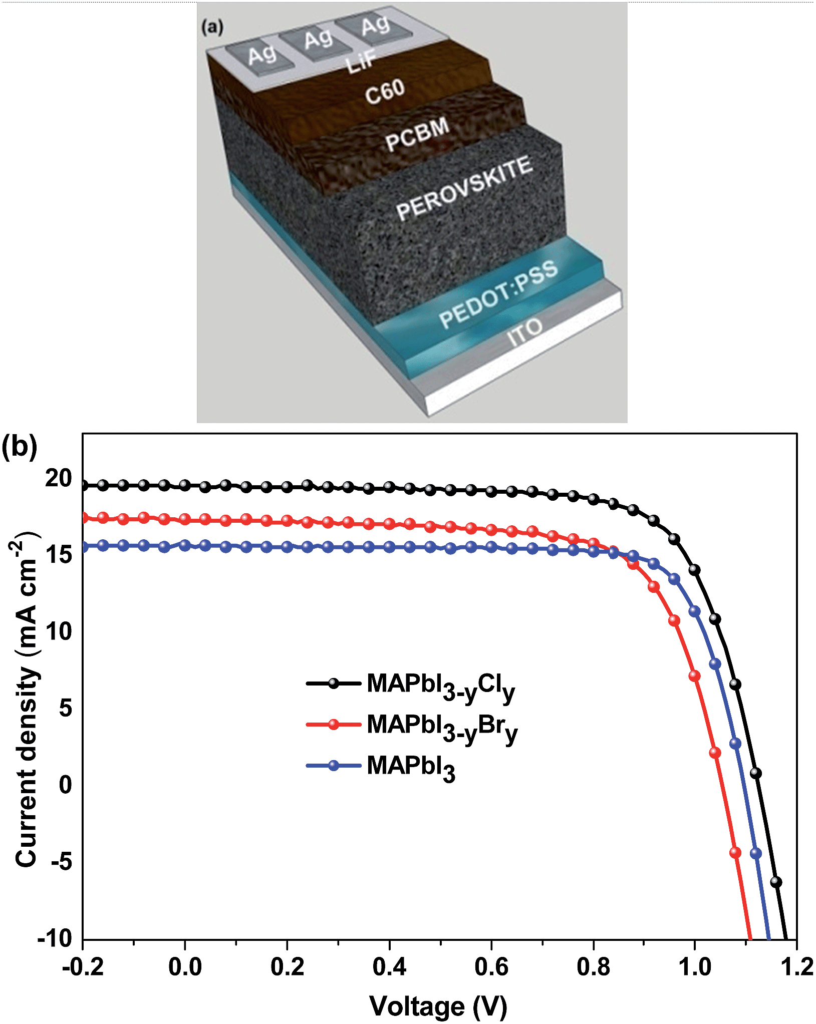 | ||
| Fig. 1 (a) Schematic architecture of planar heterojunction PSCs. (b) J–V characteristics of MAPbI3, MAPbI3−yCly, and MAPbI3−yBry-based PSCs. The devices were tested under AM1.5G illumination (100 mW cm−2). Each J–V curve is for the best device among 12 PSCs fabricated in two batches. | ||
FA+ organic cations are then incorporated for the preparation of MA1−xFAxPbI3−yCly-based PSCs. The PCE of the devices was optimized by adjusting the FAI-to-MAI ratio as well as the annealing duration of the perovskite layer. The incorporation of FA+ into MAPbI3−yCly affects the properties of the perovskite films and the performance of the PSCs (Fig. 2 and Table S1†). As the FA+ loading increases, the Jsc value increases (Fig. 2b). The maximum Jsc appears at 20 mol% of FA+. The Voc of the devices slowly decreases with the increase of the FA+ loading, and the FF value slightly increases with the increasing FAI content when the molar FAI content is less than 40% (Fig. 2c). At the optimal photovoltaic efficiency of 18.14%, the FAI/MAI ratio is 20 mol%. This corresponds to the perovskite of MA0.80FA0.20PbI3−yCly. As shown Fig. 1d, the device performance is highly sensitive to the annealing temperature of the perovskite layer. When the perovskite films are annealed between 90 °C and 110 °C, the PCEs of the PSCs are higher than 15%. The PCE value decreases when the perovskite films are annealed at either higher or lower temperature (Table S2†).
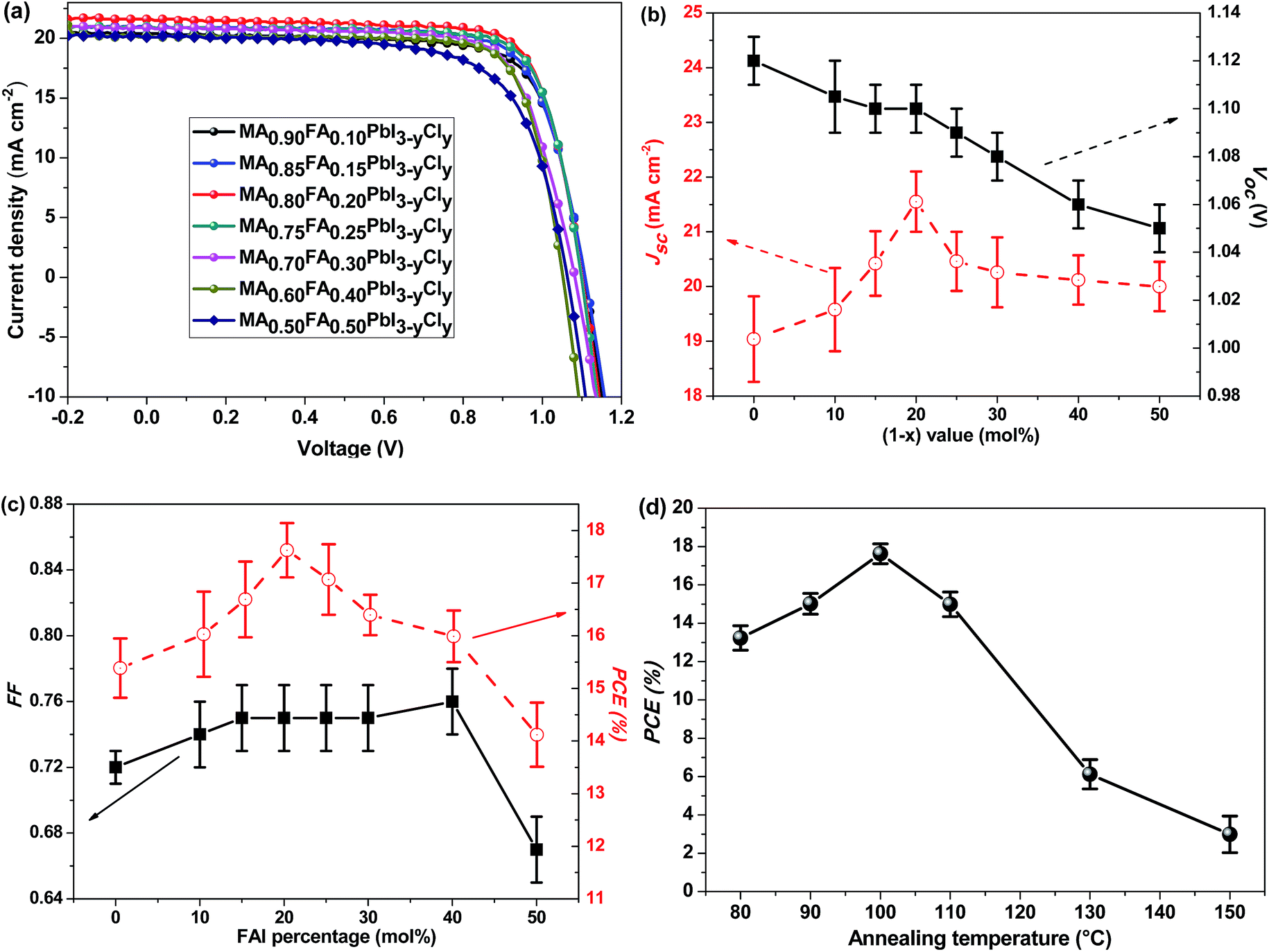 | ||
| Fig. 2 (a) J–V curves, (b) Jsc and Voc plots, (c) FF and PCE plots of MA1−xFAxPbI3−yCly-based PSCs at different FAI molar percentages. (d) PCEs of the optimized MA0.80FA0.20PbI3−yCly PSCs at different annealing temperatures of the perovskite layer. The devices were tested under AM1.5G illumination (100 mW cm−2). Each J–V curve is for the best device among 12 PSCs fabricated in two batches. | ||
In order to understand the Cl doping effect on the photovoltaic performance, control PSCs with MA0.80FA0.20PbI3 were also fabricated and characterized (Table 2 and Fig. S1†). All the photovoltaic parameters, including Voc, Jsc and FF of MA0.80FA0.20PbI3 PSCs, are lower than those of MA0.80FA0.20PbI3−yCly. The highest PCE of the former is only 13.78%. Through a comparison of the PCEs of all the PSCs in this study (Tables 1 and 2), it was found that the MA0.80FA0.20PbI3−yCly-based PSCs significantly outperform the other PSCs. The high efficiency is due to the combination of the high Jsc (21.55 ± 0.55 mA cm−2), Voc (1.100 ± 0.010 V) and FF (0.75 ± 0.02), which is achieved by the synergetic effects of FA+ and Cl− dopings.
| Perovskite | Precursors | Film thickness (nm) | Annealing (min)/temperature (°C) | J sc (mA cm−2) | V oc (V) | FFa | PCEa [best (average)] (%) | R s (best device) (Ω cm2) | R sh (best device) (kΩ cm2) | J sc (mA cm−2) |
|---|---|---|---|---|---|---|---|---|---|---|
| a Each average result is derived from 12 PSCs from two batches. b Each average result is derived from 5 PSCs. c Calculated from the IPCE curves. | ||||||||||
| MA0.80FA0.20PbI3−yCly | 1.26 M PbI2, 0.14 M PbCl2, 1.08 M MAI, 0.27 M FAI | ∼280 | 15/100 | 21.55 ± 0.55 | 1.100 ± 0.010 | 0.75 ± 0.02 | 18.14 (17.45) | 3.65 ± 0.95(4.57) | 706 ± 694(270) | 19.34 |
| MA0.80FA0.80PbI3 | 1.4 M of PbI2, 1.08 M MAI, 0.27 M FAI | ∼260 | 15/100 | 18.51 ± 1.28 | 0.990 ± 0.030 | 0.70 ± 0.03 | 13.78 (12.89) | 5.10 ± 1.70 (6.85) | 1703 ± 1676(3379) | 16.85 |
The hysteresis in the J–V curves of the PSCs is also investigated since different scanning directions may induce overestimation or underestimation of the device performance.44–46 The J–V curves of the PSCs were recorded along the reverse (from 1.2 V to −0.2 V) and forward (from −0.2 V to 1.2 V) scan directions at a scan rate of 40 mV s−1 under AM1.5G illumination. The hysteresis of the J–V curves depends on the annealing temperature. When the MA0.80FA0.20PbI3−yCly layer was annealed below 110 °C, no hysteresis was observed on the J–V curves of the PSCs along the scan directions (Fig. 3a and S2†). When the MA0.80FA0.20PbI3−yCly layer was annealed at 130–150 °C, hysteresis was observed on the J–V curves (Fig. 3b and S2†). The effect of the annealing temperature on the hysteresis is attributed to their effect on the morphology of the perovskite layer. Annealing at high temperature can give rise to a very rough perovskite surface (Fig. S8†), which can induce charge trapping centers. Hence, the devices annealed at high temperatures show a distinct hysteresis behaviour probably due to the accumulation of charges at the grain boundaries and/or filling of the interfacial or surface trap states.22,47 We also examined the hysteresis in the J–V curves of the PSCs employing the other active layers (Fig. S3†). The hysteresis is dependent on the composition of the perovskite layer as well.
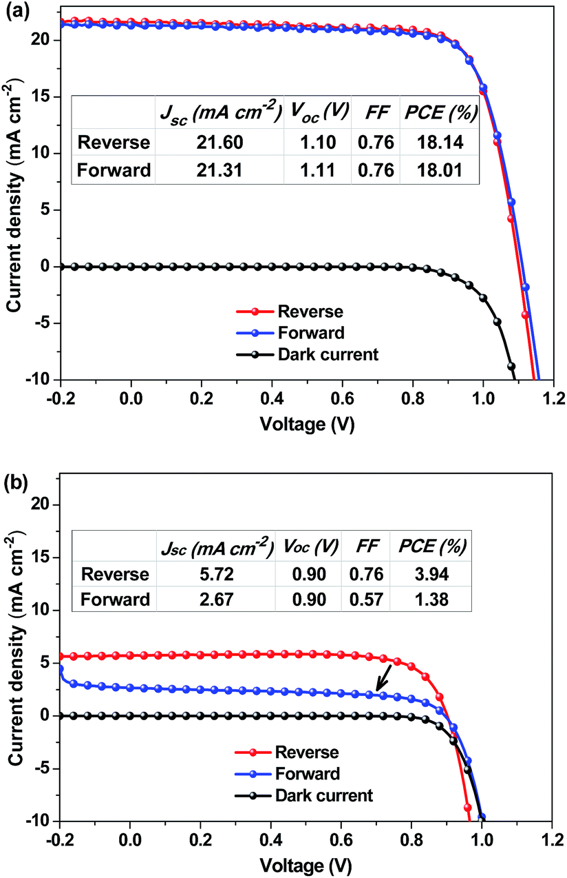 | ||
| Fig. 3 J–V characteristics of ITO/PEDOT:PSS/MA0.80FA0.20PbI3−yCly/PCBM/C60/LiF/Ag PSCs with the MA0.80FA0.20PbI3−yCly layer annealed at (a) 100 °C and (b) 150 °C. The J–V curves belong to the best performing devices among 12 PSCs fabricated in two batches. | ||
Various characterizations are performed to understand the MA0.80FA0.20PbI3−yCly-based PSCs. Fig. 4 presents the internal photo-electron conversion efficiency (IPCE) measurements. The Jsc values of the PSCs calculated in terms of the IPCEs are provided in Tables 1 and 2. They are very well consistent with those obtained from the J–V curves. The IPCE of MA0.80FA0.20PbI3−yCly-based PSCs is higher than 75% in the ranges of 430–630 nm and 670–730 nm. In addition, its IPCE shifts to red in comparison to PSCs with MAPbI3−yCly and MAPbI2.70Br0.30. The red shift can be attributed to the lattice expansion effect by FA+ doping.34
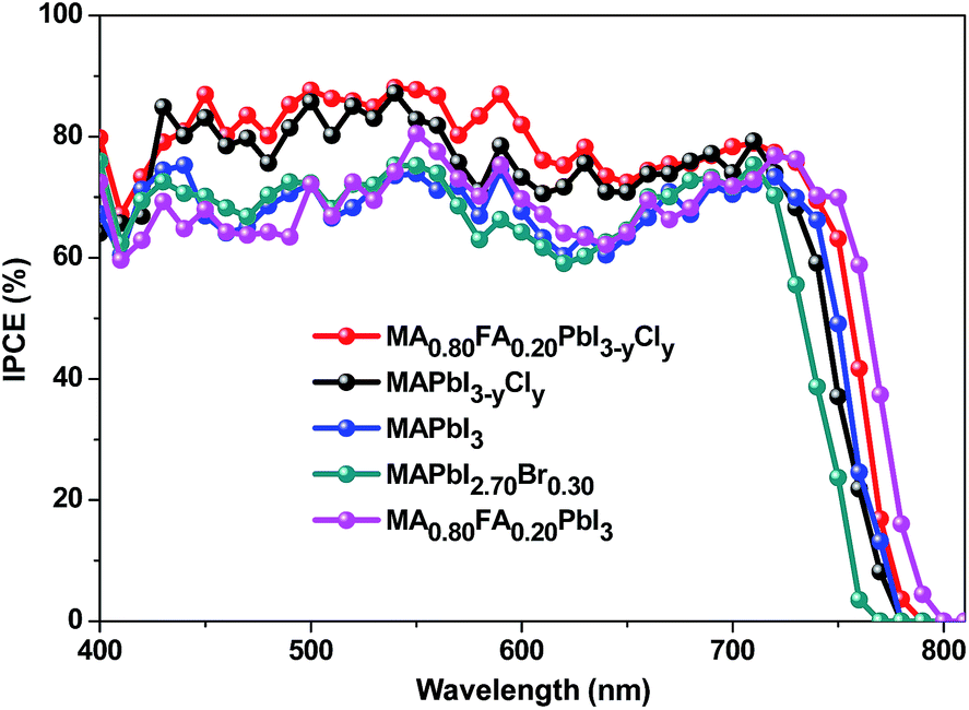 | ||
| Fig. 4 IPCE curves of ITO/PEDOT:PSS/perovskite/PCBM/C60/LiF/Ag PSCs with different perovskites. | ||
Fig. 5a shows the X-ray diffraction patterns of the perovskite thin films with different compositions. As can be seen from the diffraction patterns, all of the precursors are successfully converted to the corresponding perovskites. We also confirm the successful formation of MA0.80FA0.20PbI3−yCly perovskite at different annealing temperatures (Fig. S4†). The diffraction peaks at 14.2°, 28.7°, 32.1° and 43.3° are assigned to the (110), (220), (310), and (116) crystal planes of the tetragonal perovskite phase, respectively. There is a trace amount of PbI2 as indicated by the small peak at 13.0°.48–50 The slight excess of PbI2 inside the perovskite thin film, which is purposefully introduced, can passivate the perovskite grain boundaries and thus suppresses the charge recombination.48 It can also have a beneficial effect in reducing the hysteresis of the I–V characteristics and ion migration.51 Lattice parameters of the tetragonal perovskite phases are calculated to investigate the impact of the halide and/or the organic cation dopings on the crystal structure of the neat MAPbI3 (eqn (S1)†). The calculated unit cell lengths (a = 8.8073 nm and c = 12.5354) of MAPbI3 conform with those of the single crystal XRD data.16 For MAPbI3−yCly and MAPbI2.70Br0.30, the unit cell lengths are calculated as a = 8.7952 nm and c = 12.5192 nm, and a = 8.7711 nm and c = 12.4814 nm, respectively. These results suggest that doping of MAPbI3 with Cl− or Br−, which are smaller ions than I−, results in lattice shrinkage. Conversely, the FA+ doping gives rise to lattice expansion so that the calculated unit cell lengths are a = 8.8439 nm and c = 12.5899 nm, and a = 8.8439 nm and c = 12.5844 nm, respectively for MA0.80FA0.20PbI3 and MA0.80FA0.20PbI3−yCly compositions. In addition, the lattice stretches more with the increasing FA+ mol ratio (eqn (S1)†). This fact is observable from the right or left shift of the parent MAPbI3 perovskite peak upon the halide and/or the FA+ dopings (Fig. 5b and S5†).
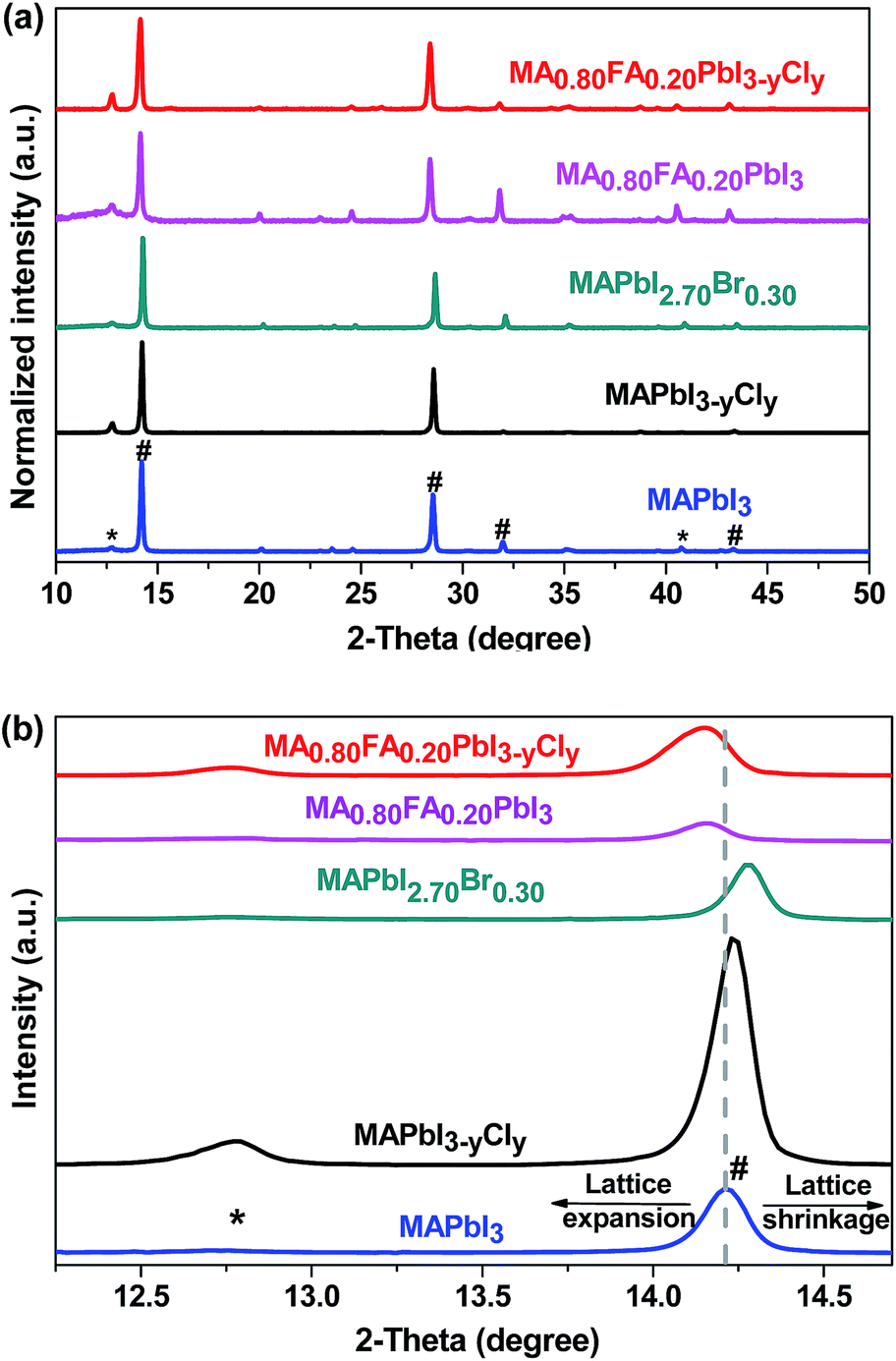 | ||
| Fig. 5 XRD patterns of perovskite films with different compositions. The patterns indicated with * are from PbI2 and the ones with # are due to perovskites. | ||
A significant problem regarding formamidinium-based lead halides is their polymorphism at room temperature. The black trigonal α-phase of FAPbI3 can be formed at a temperature above 130 °C, and it tends to convert to a yellow hexagonal δ-phase at lower temperatures.29 As shown by Jeon et al.,33 a black FAPbI3 powder completely returns to the yellow powder after being stored in air for just 10 h. The yellow FAPbI3 phase has a large indirect band gap of 2.48 eV30 and it is thus not suitable for photovoltaic application. In this study, we found that no δ-phase is formed in MA1−xFAxPbI3−yCly thin films with x = 0.2, 0.3 and 0.4 after a week as evidenced by XRDs (Fig. S6†).33 Previous studies also demonstrate that the black phase of FA+-based perovskites is stabilized by mixing with MA+.29,31 Even at the MA+ molar percentage of 15%, no δ-phase is formed in the temperature range of 25–250 °C. The smaller MA+ has a dipole moment of 2.3 D which is about ten times higher than that of FA+ (0.21 D).52 Hence, the incorporation of MA+ into the α-FAPbI3 structure can induce the formation of stronger I–H hydrogen bonds and this can stabilize the 3D arrangement of the PbI6 octahedra. Moreover, the stronger interaction between MA+ and PbI6 results in an increase in the Madelung energy that is the electrostatic energy among all the atoms, which consequently enhances the stability of the system.29
The morphology and surface texture of the perovskites are examined by SEM and AFM (Fig. 6). The SEM images reveal that all the perovskites of different compositions annealed at 100 °C can form pinhole-free, uniform and dense films that fully cover the PEDOT:PSS layer. The grains have a size of around 200 nm. The crystalline structures with a bright contrast in the SEM images can be the less conductive PbI2 species. The excess PbI2 species are located at the grain boundaries, and they are beneficial in suppressing the charge recombination.48 The Cl-free perovskites have very smooth surfaces, while the MA0.80FA0.20PbI3−yCly and MAPbI3−yCly thin films with Cl doping exhibit an irregular grain morphology. The MA0.80FA0.20PbI3−yCly and MAPbI3−yCly films have root-mean-square roughness (RRMS) values above 10 nm. The Cl doping increases the surface roughness of the perovskite films.
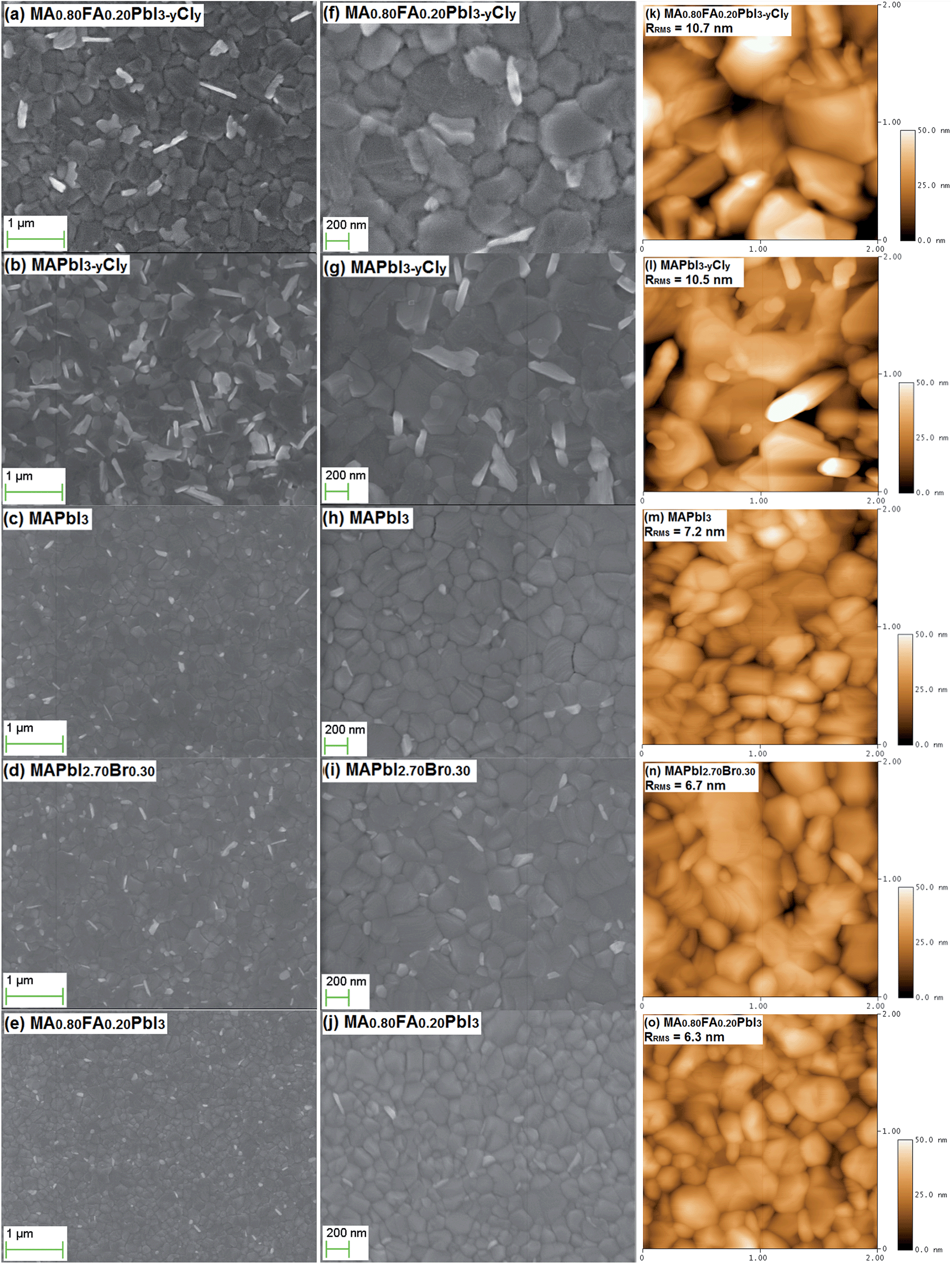 | ||
| Fig. 6 SEM and AFM images of MA0.80FA0.20PbI3−yCly, MAPbI3−yCly, MAPbI3, MAPbI2.70Br0.30, and MA0.80FA0.20PbI3 thin films. The perovskite films were annealed at 100 °C. The scale bars are 1 μm for the SEM images of (a–e) and 200 nm for the SEM images of (f–j). The scale is 2 μm and the height scale bar is 50 nm for the AFM images (k–o). The RRMS values are indicated on the AFM images. | ||
The formation of FA+-containing perovskites via the one-step solution method requires an annealing process at 140–170 °C due to the larger size of FA+ than that of MA+.34–36 Nonetheless, MA1−xFAxPbI3−yCly with the FA+ molar percentage up to 50% can be formed after annealing only at 100 °C in this study (Table S1†). In order to understand the benefits of the low annealing temperature, SEM and AFM images of MA0.80FA0.20PbI3−yCly-based thin films prepared at different annealing temperatures are further investigated (Fig. 6a, f and S8†). The MA0.80FA0.20PbI3−yCly thin films annealed at 80 °C, 90 °C, and 100 °C have a smooth surface with the RRMS values of 9.1–10.7 nm. Pinholes can be observed for the MA0.80FA0.20PbI3−yCly films annealed at 80 °C and 90 °C. This is the reason for the low FF value of the corresponding PSCs (Table S2†). The perovskite films become very rough (RRMS > 18.7 nm) when the annealing temperature is 110 °C or higher. Pinholes can be observed for the films annealed at 130 °C and 150 °C as well. The pinholes lower the photovoltaic performance of the corresponding PSCs (Table S2†). The annealing at high temperature can induce the excess sublimation/evaporation of FAX or MAX (X = I, Br or Cl) and/or the decomposition of FA+-containing perovskite.36 Eperon et al.35 also confirmed the effect of annealing temperature on the morphology of the FA+-containing perovskite films.
The UV-vis absorption spectra of the perovskite thin films with different compositions are presented in Fig. 7a. The absorption onset of MAPbI3 is 785.0 nm, which indicates an optical band gap of 1.58 eV, which is consistent with the reported values (1.55–1.61 eV).18,53 As the electronegativity of the halogen atoms in organometal lead perovskites increases, the covalent characteristic of the halogen bonding with the lead decreases. Hence, the light absorption of MAPbI3 shifts to blue when the iodide is replaced with bromine or chlorine.21 That is why, the band gap of MAPbI3 increases by ∼0.04 eV when 10 mol% of the iodide is replaced with bromine. Although the Cl doping does not affect the band gap of MAPbI3 as reported in the literature,1,24 we found that MAPbI3−yCly exhibits a slightly larger band gap than MAPbI3 (Fig. 7a). This might be due to the trace amount of Cl− remaining inside the PbI6 octahedron. The band gap of MA0.80FA0.20PbI3 is ∼0.02 eV, smaller than that of MAPbI3. As the FA+ mol ratio increases, the band gap of MA1−xFAxPbI3−yCly decreases (Fig. 7b). Interestingly, MAPbI3 and MA0.80FA0.20PbI3−yCly have the same absorption onset (Fig. 7a). This can be attributed to the fact that the band tuning effects of FA+ and Cl− ions cancel each other. The band gap of MA1−xFAxPbI3−yCly also depends on the annealing temperature. As the annealing temperature increases, the band gap of the perovskite decreases (Fig. S9†). Presumably, more MAX (X = I or Cl) forms as a result of the sublimation/evaporation and/or the decomposition of the formed perovskite at elevated temperatures. This process results in the formation of MA1−xFAxPbI3−yCly with a higher FA+ molar percentage.
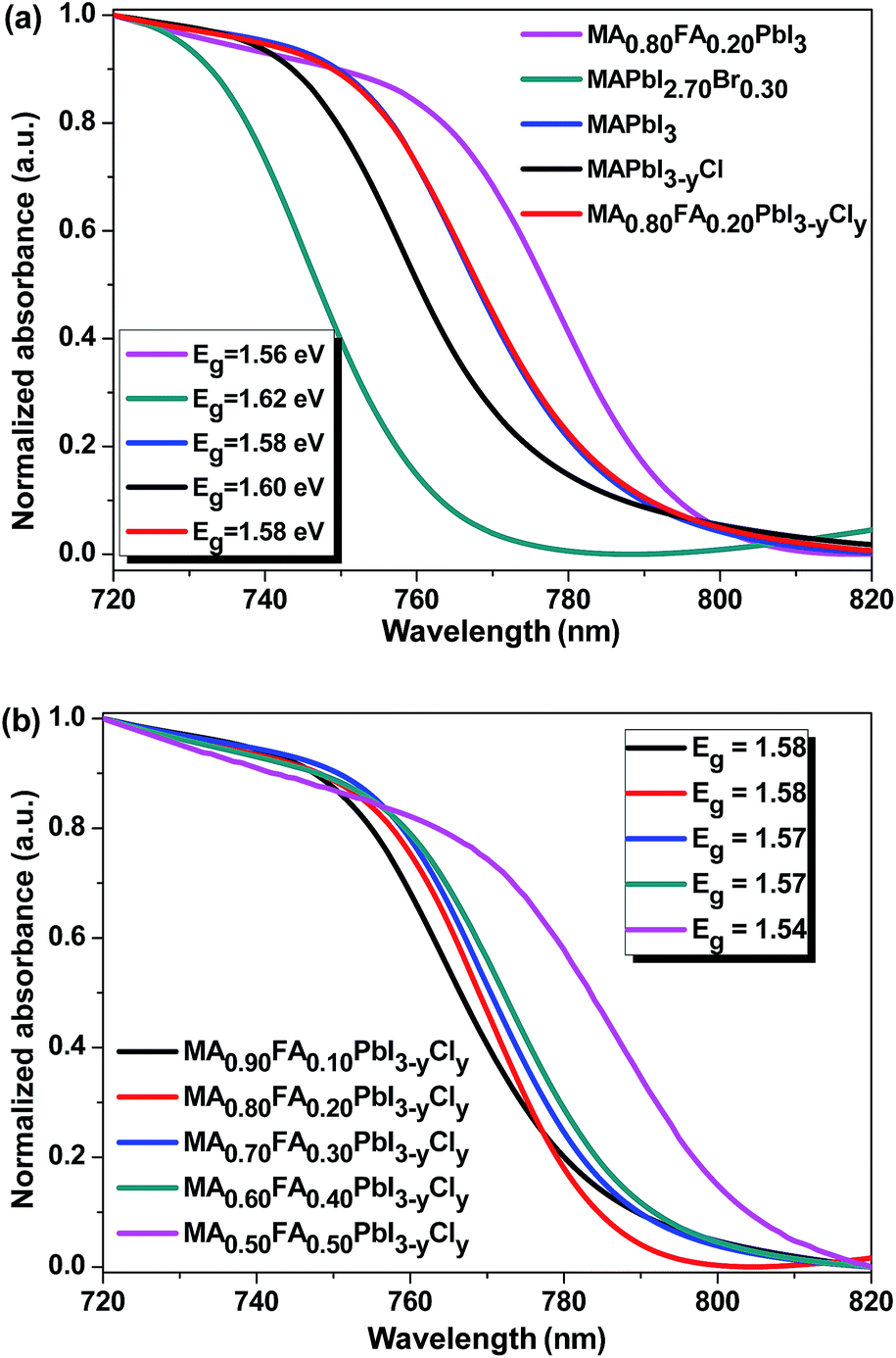 | ||
| Fig. 7 UV-vis absorption spectra of the perovskite films with different compositions. The inset shows the optical band gaps of the perovskite films. | ||
Time-resolved PL measurements were conducted to investigate the photo-conversion processes of the perovskites with different compositions. The carrier diffusion lengths were calculated according to the 1D diffusion model as described by Xing et al.54 The time-resolved PL measurement conditions and fitting methodology are provided in the experimental and ESI parts (eqn (S2)†). Briefly, PCBM as an electron-extraction layer or PEDOT:PSS as a hole-extraction layer is used for the investigation of electron or hole dynamics. In terms of the results for the samples of bare glass/perovskites, glass/perovskites/PCBM and glass/PEDOT:PSS/perovskites, the carrier distribution n(z,t) throughout the perovskite thin films can be described by this equation,
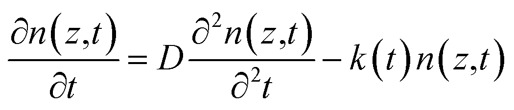
![[thin space (1/6-em)]](https://www.rsc.org/images/entities/char_2009.gif) exp(−αz), where α is the linear absorption coefficient of the thin films at the excitation wavelength of 515 nm. Under the assumption of a perfect quencher case, all the electrons or holes are quenched at the interface of the quenching layer at an infinite quenching rate. A minimum value of D is fitted by using eqn (S2).† The diffusion length (LD) is then derived in terms of LD = (Dτ0)1/2, where τ0 is the PL lifetime in the absence of quenchers. The PL decay and bi-exponentially fitted curves of the thin films are presented in Fig. 8. The fitted parameters are summarized in Table 3.
exp(−αz), where α is the linear absorption coefficient of the thin films at the excitation wavelength of 515 nm. Under the assumption of a perfect quencher case, all the electrons or holes are quenched at the interface of the quenching layer at an infinite quenching rate. A minimum value of D is fitted by using eqn (S2).† The diffusion length (LD) is then derived in terms of LD = (Dτ0)1/2, where τ0 is the PL lifetime in the absence of quenchers. The PL decay and bi-exponentially fitted curves of the thin films are presented in Fig. 8. The fitted parameters are summarized in Table 3.
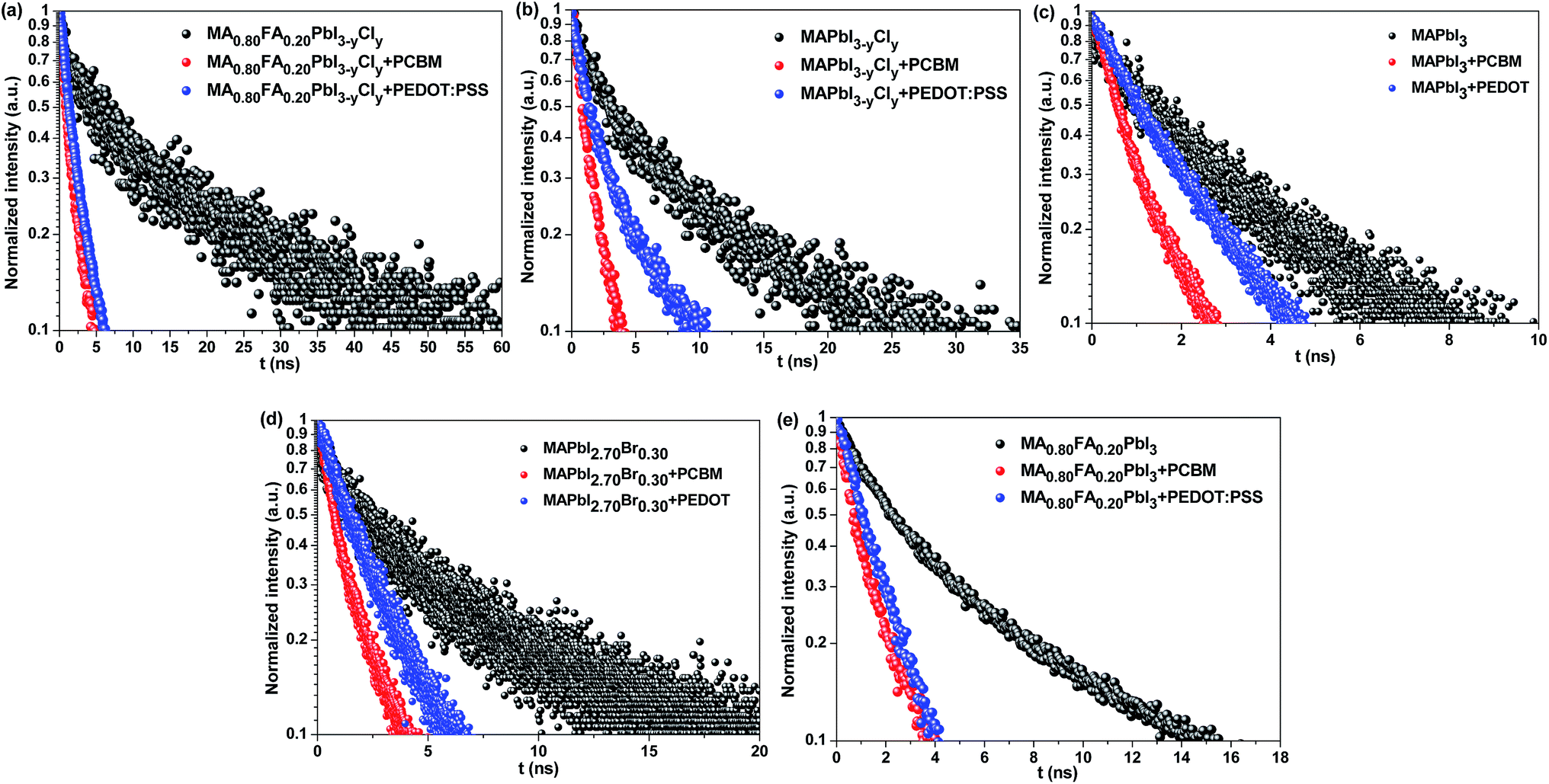 | ||
| Fig. 8 Time-resolved PL curves of (a) MA0.80FA0.20PbI3−yCly, (b) MAPbI3−yCly, (c) MAPbI3, (d) MAPbI2.70Br0.30, and (e) MA0.80FA0.20PbI3 on glass (black) with an electron extracting PCBM layer (red) or with a hole extracting PEDOT:PSS layer (blue). | ||
| A 1 | τ 1 (ns) | A 2 | τ 2 (ns) | D h (cm2 s−1) | L D−h (nm) | D e (cm2 s−1) | L D−e (nm) | |
|---|---|---|---|---|---|---|---|---|
| a D h: hole diffusion coefficient; De: electron diffusion coefficient; LD−h: hole diffusion length; LD−e: electron diffusion length. | ||||||||
| MA0.80FA0.20PbI3−yCly | 0.59 | 5.05 | 0.41 | 30.78 | 1.20 × 10⁻¹ | 557 | 1.70 × 10⁻¹ | 662 |
| MAPbI3−yCly | 0.57 | 2.88 | 0.43 | 16.76 | 7.27 × 10⁻² | 321 | 1.99 × 10⁻¹ | 531 |
| MAPbI3 | 0.58 | 1.44 | 0.42 | 5.88 | 9.51 × 10⁻² | 213 | 2.15 × 10⁻¹ | 320 |
| MAPbI2.70Br0.30 | 0.59 | 2.16 | 0.41 | 13.92 | 9.07 × 10⁻² | 327 | 1.59 × 10⁻¹ | 433 |
| MA0.80FA0.20PbI3 | 0.72 | 2.59 | 0.28 | 15.31 | 1.57 × 10⁻¹ | 365 | 1.18 × 10⁻¹ | 358 |
Among the perovskites with different compositions, MA0.80FA0.20PbI3−yCly exhibits the longest electron (662 nm) and hole (557 nm) diffusion lengths, which is followed by MAPbI3−yCly (LD−e = 531 nm, LD−h = 321 nm) (Table 3). These results imply that the Cl doping can increase the charge carrier diffusion lengths. As shown in Tables 1 and 2, the Cl doping also enhances Voc of the PSCs. These results are consistent with those reported in the literature.2,26,55 Although the Br doping of MAPbI3 also increases the charge carrier diffusion lengths, the electron (433 nm) and hole (327 nm) diffusion lengths are significantly lower than those with Cl doping. By comparing the optical physics of MA0.80FA0.20PbI3−yCly with MAPbI3−yCly and MA0.80FA0.20PbI3 with MAPbI3, we can conclude that the FA+ organic cations can also increase the charge diffusion lengths. This can be attributed to the effects of the large FA+ cations on the lattice and the band structure of the perovskites. Eperon et al. also reported that the charge carrier diffusion length in FAPbI3 is longer than that in MAPbI3.34
Conclusions
In summary, we reported a new perovskite, MA1−xFAxPbI3−yCly, and its corresponding PSCs for the first time. MA1−xFAxPbI3−yCly thin films can be formed by annealing at a relatively low temperature of 80–110 °C. The MA0.80FA0.20PbI3−yCly-based planar heterojunction PSCs can exhibit a high photovoltaic efficiency of up to 18.14% with Jsc, Voc, and FF values of 21.55 ± 0.55 mA cm−2, 1.100 ± 0.010 V, and 0.75 ± 0.02, respectively. The efficiency is significantly higher than that of the control PSCs using MAPbI3, MAPbI3−yCly, MAPbI3−yBry, and MA1−xFAxPbI3 as the active layers. The high photovoltaic performance of MA0.80FA0.20PbI3−yCly-based PSCs is attributed to the synergetic effects of the organic cation doping and halide doping. They can lead to the formation of pinhole-free and smooth perovskite films through annealing at low temperature and the increase in the charge diffusion lengths.Experimental
Materials and chemicals
Patterned indium tin oxide (ITO) glass substrates (15 ohm □−1) were obtained from the NSG group. Poly(3,4-ethylenedioxythiophene):poly(styrene sulfonate) (PEDOT:PSS, Clevios P VP Al 4083) was supplied by Heraeus Holding GmbH. Methylammonium iodide (MAI) and formamidinium iodide (FAI) were received from Dyesol Ltd. [6,6]-phenyl-C61-butyric acid methyl ester (PCBM) was obtained from Nano-C Inc. Other chemicals, including lead(II) iodide (PbI2: 99.999% purity), lead(II) chloride (PbCl2: 99.999% purity), lead(II) bromide (PbBr2: 99.999% purity), C60 (98% purity), chlorobenzene (anhydrous, 99.8% purity), dimethyl sulfoxide (DMSO, anhydrous, ≥99.9% purity), γ-butyrolactone (GBL, ≥99% purity), toluene (anhydrous, 99.5% purity), LiF (≥99% purity), and silver (Ag shot, ≥99.99% purity), were purchased from Sigma-Aldrich. All materials were used as received without further purification.Fabrication and characterization of PSCs
The device architecture is shown in Fig. 1a. The devices were fabricated through the following process. ITO glass substrates were cleaned by sonication successively in detergent, deionized water, acetone, and isopropanol. The sonication time was 20 min for each cleaning. They were then dried with N2 flow and then treated in a UV-ozone for 15 min. The hole transporting layer, PEDOT:PSS, with a thickness of ∼20 nm was spin-coated onto the ITO substrates at 8k rpm for 35 s and then annealed at 140 °C for 15 min in air. The ITO substrates coated with PEDOT:PSS were then transferred into a glovebox filled with N2 to coat the perovskite and PCBM layers. The perovskite precursor solution was prepared by dissolving 1.4 M of PbI2 + PbCl2 and 1.35 M of MAI + FAI in a co-solvent of GBL/DMSO (3:7 vol. ratio). The total concentration of PbI2 and PbCl2 is 1.4 M, and that of MAI and FAI is 1.35 M. The substrates and the precursor solution were pre-heated at 85 °C, and then the precursor solution was coated at 1k rpm for 20 s. 1 mL toluene was dripped after 20 s at 4k rpm. It was then annealed at 100 °C for 15 min. The thickness of the perovskite layer was around 280 nm as determined using a surface step profiler. The electron transporting layer was deposited on the perovskite layer by spin coating a chlorobenzene solution of 20 mg mL−1 PCBM at 2k rpm for 90 s. The devices were completed by the thermal deposition of C60 (20 nm thick), LiF (0.6 nm thick), and Ag (100 nm thick) at a vacuum of <1 × 10⁻⁶ Torr. The PSCs were encapsulated with a UV-curable epoxy and glass sheets in the glovebox. Each device had an active area of 0.11 cm2. A mask was used during the photovoltaic tests.
The devices were tested under ambient conditions. A Keithley 2400 source/meter unit was used to record the J–V curves of the PSCs. The photocurrent was measured for the devices under AM1.5 illumination (100 mW cm−2), which was calibrated using a standard Si photodiode detector. The IPCE spectra were obtained using an IPCE setup consisting of a Xenon lamp (Oriel, 300 W) as the light source, a Cornerstone 260 Oriel 74125 monochromator, and a lock-in amplifier (SR830 by the Stanford Research Corp). The light source was calibrated with a Si-based diode (J115711-1-Si detector).
Thin film characterization
UV-visible absorption spectra were obtained using a Shimadzu UV-1800 spectrophotometer. The X-ray diffraction (XRD) patterns were recorded with a Bruker D8 Advance XRD Instrument. Film thickness values were determined employing a surface profilometer (KLA Tencor, Alpha-Step IQ). Photoluminescence (PL) spectra were obtained using a LS 55 Fluorescence Spectrometer (PerkinElmer) with an excitation wavelength of 300 nm. Electron scanning microscopy (SEM) and atomic force microscopy (AFM) images were acquired with a Zeiss Supra-40 SEM and a Veeco NanoScope IV Multi-Mode AFM operated in the tapping mode, respectively. For the time-resolved photoluminescence measurements, the perovskite thin films were excited by a 515 nm laser. The excitation laser had a frequency of 100 kHz and a pulse duration of 200 fs. The scattered excitation light was eliminated with a 532 nm long pass filter. After filtering with a 776 ± 10 nm band pass filter, the emission of the samples was collected by an avalanche photon diode (Micro photon device by the PicoQuant). The PL kinetics were measured using a time-correlated single photon counting module (TCSPC PicoHarp 300 by the PicoQuant) with a time window of 260 ns.Acknowledgements
This research work was financially supported by a research grant from the Ministry of Education, Singapore (R284-000-147-112).References
- M. M. Lee, J. Teuscher, T. Miyasaka, T. N. Murakami and H. J. Snaith, Science, 2012, 338, 643 CrossRef CAS PubMed.
- S. D. Stranks, G. E. Eperon, G. Grancini, C. Menelaou, M. J. Alcocer, T. Leijtens, L. M. Herz, A. Petrozza and H. J. Snaith, Science, 2013, 342, 341 CrossRef CAS PubMed.
- A. Mei, X. Li, L. Liu, Z. Ku, T. Liu, Y. Rong, M. Xu, M. Hu, J. Chen, Y. Yang, M. Grätzel and H. Han, Science, 2014, 345, 295 CrossRef CAS PubMed.
- N. J. Jeon, J. H. Noh, Y. C. Kim, W. S. Yang, S. Ryu and S. I. Seok, Nat. Mater., 2014, 13, 897 CrossRef CAS PubMed.
- J. Burschka, N. Pellet, S.-J. Moon, R. Humphry-Baker, P. Gao, M. K. Nazeeruddin and M. Gratzel, Nature, 2013, 499, 316 CrossRef CAS PubMed.
- M. Liu, M. B. Johnston and H. J. Snaith, Nature, 2013, 501, 395 CrossRef CAS PubMed.
- W. Nie, H. Tsai, R. Asadpour, J.-C. Blancon, A. J. Neukirch, G. Gupta, J. J. Crochet, M. Chhowalla, S. Tretiak, M. A. Alam, H.-L. Wang and A. D. Mohite, Science, 2015, 347, 522 CrossRef CAS PubMed.
- W. S. Yang, J. H. Noh, N. J. Jeon, Y. C. Kim, S. Ryu, J. Seo and S. I. Seok, Science, 2015, 348, 1234 CrossRef CAS PubMed.
- D. Bi, W. Tress, M. I. Dar, P. Gao, J. Luo, C. Renevier, K. Schenk, A. Abate, F. Giordano, J.-P. Correa Baena, J.-D. Decoppet, S. M. Zakeeruddin, M. K. Nazeeruddin, M. Grätzel and A. Hagfeldt, Sci. Adv., 2016, 2, e1501170 Search PubMed.
- H. Zhou, Q. Chen, G. Li, S. Luo, T.-b. Song, H.-S. Duan, Z. Hong, J. You, Y. Liu and Y. Yang, Science, 2014, 345, 542 CrossRef CAS PubMed.
- Y. Shao, Y. Yuan and J. Huang, Nature Energy, 2016, 1, 15001 CrossRef.
- H. Kim, K.-G. Lim and T.-W. Lee, Energy Environ. Sci., 2016, 9, 12 CAS.
- M. A. Green, Y. Jiang, A. M. Soufiani and A. Ho-Baillie, J. Phys. Chem. Lett., 2015, 6, 4774 CrossRef CAS PubMed.
- F. Li, C. Ma, H. Wang, W. Hu, W. Yu, A. D. Sheikh and T. Wu, Nat. Commun., 2015, 6, 8238 CrossRef PubMed.
- Q. Dong, Y. Fang, Y. Shao, P. Mulligan, J. Qiu, L. Cao and J. Huang, Science, 2015, 347, 967 CrossRef CAS PubMed.
- D. Shi, V. Adinolfi, R. Comin, M. Yuan, E. Alarousu, A. Buin, Y. Chen, S. Hoogland, A. Rothenberger, K. Katsiev, Y. Losovyj, X. Zhang, P. A. Dowben, O. F. Mohammed, E. H. Sargent and O. M. Bakr, Science, 2015, 347, 519 CrossRef CAS PubMed.
- A. Miyata, A. Mitioglu, P. Plochocka, O. Portugall, J. T.-W. Wang, S. D. Stranks, H. J. Snaith and R. J. Nicholas, Nat. Phys., 2015, 11, 582 CrossRef CAS.
- A. Kojima, K. Teshima, Y. Shirai and T. Miyasaka, J. Am. Chem. Soc., 2009, 131, 6050 CrossRef CAS PubMed.
- C. Roldan-Carmona, P. Gratia, I. Zimmermann, G. Grancini, P. Gao, M. Graetzel and M. K. Nazeeruddin, Energy Environ. Sci., 2015, 8, 3550 CAS.
- Z. Xiao, Y. Yuan, Q. Wang, Y. Shao, Y. Bai, Y. Deng, Q. Dong, M. Hu, C. Bi and J. Huang, Mater. Sci. Eng., R, 2016, 101, 1 CrossRef.
- P. Gao, M. Grätzel and M. K. Nazeeruddin, Energy Environ. Sci., 2014, 7, 2448 CAS.
- S. Brittman, G. W. Adhyaksa and E. C. Garnett, MRS Commun., 2015, 5, 7 CrossRef CAS PubMed.
- Q. Chen, H. Zhou, Y. Fang, A. Z. Stieg, T.-B. Song, H.-H. Wang, X. Xu, Y. Liu, S. Lu, J. You, P. Sun, J. McKay, M. S. Goorsky and Y. Yang, Nat. Commun., 2015, 6, 7269 CrossRef CAS PubMed.
- S. Colella, E. Mosconi, P. Fedeli, A. Listorti, F. Gazza, F. Orlandi, P. Ferro, T. Besagni, A. Rizzo, G. Calestani, G. Gigli, F. De Angelis and R. Mosca, Chem. Mater., 2013, 25, 4613 CrossRef CAS.
- E. L. Unger, A. R. Bowring, C. J. Tassone, V. L. Pool, A. Gold-Parker, R. Cheacharoen, K. H. Stone, E. T. Hoke, M. F. Toney and M. D. McGehee, Chem. Mater., 2014, 26, 7158 CrossRef CAS.
- J. Liu and O. V. Prezhdo, J. Phys. Chem. Lett., 2015, 6, 4463 CrossRef CAS PubMed.
- J. H. Noh, S. H. Im, J. H. Heo, T. N. Mandal and S. I. Seok, Nano Lett., 2013, 13, 1764 CrossRef CAS PubMed.
- C. C. Stoumpos, C. D. Malliakas and M. G. Kanatzidis, Inorg. Chem., 2013, 52, 9019 CrossRef CAS PubMed.
- A. Binek, F. C. Hanusch, P. Docampo and T. Bein, J. Phys. Chem. Lett., 2015, 6, 1249 CrossRef CAS PubMed.
- Z. Wang, Y. Zhou, S. Pang, Z. Xiao, J. Zhang, W. Chai, H. Xu, Z. Liu, N. P. Padture and G. Cui, Chem. Mater., 2015, 27, 7149 CrossRef CAS.
- C. Yi, J. Luo, S. Meloni, A. Boziki, N. Ashari-Astani, C. Gratzel, S. M. Zakeeruddin, U. Rothlisberger and M. Gratzel, Energy Environ. Sci., 2016, 9, 656 CAS.
- J. Liu, Y. Shirai, X. Yang, Y. Yue, W. Chen, Y. Wu, A. Islam and L. Han, Adv. Mater., 2015, 27, 4918 CrossRef CAS PubMed.
- N. J. Jeon, J. H. Noh, W. S. Yang, Y. C. Kim, S. Ryu, J. Seo and S. I. Seok, Nature, 2015, 517, 476 CrossRef CAS PubMed.
- G. E. Eperon, S. D. Stranks, C. Menelaou, M. B. Johnston, L. M. Herz and H. J. Snaith, Energy Environ. Sci., 2014, 7, 982 CAS.
- G. E. Eperon, D. Bryant, J. Troughton, S. D. Stranks, M. B. Johnston, T. Watson, D. A. Worsley and H. J. Snaith, J. Phys. Chem. Lett., 2015, 6, 129 CrossRef CAS PubMed.
- S. Lv, S. Pang, Y. Zhou, N. P. Padture, H. Hu, L. Wang, X. Zhou, H. Zhu, L. Zhang, C. Huang and G. Cui, Phys. Chem. Chem. Phys., 2014, 16, 19206 RSC.
- J. Seo, S. Park, Y. Chan Kim, N. J. Jeon, J. H. Noh, S. C. Yoon and S. I. Seok, Energy Environ. Sci., 2014, 7, 2642 CAS.
- L. C. Chen, J. C. Chen, C. C. Chen and C. G. Wu, Nanoscale Res. Lett., 2015, 10, 1020 Search PubMed.
- J. W. Jung, S. T. Williams and A. K. Y. Jen, RSC Adv., 2014, 4, 62971 RSC.
- K. Sun, J. Chang, F. H. Isikgor, P. Li and J. Ouyang, Nanoscale, 2015, 7, 896 RSC.
- S. Zhang, Z. Yu, P. Li, B. Li, F. H. Isikgor, D. Du, K. Sun, Y. Xia and J. Ouyang, Org. Electron., 2016, 32, 149 CrossRef.
- J. Chang, H. Zhu, B. Li, F. H. Isikgor, Y. Hao, Q. Xu and J. Ouyang, J. Mater. Chem. A, 2016, 4, 887 CAS.
- S. A. Kulkarni, T. Baikie, P. P. Boix, N. Yantara, N. Mathews and S. Mhaisalkar, J. Mater. Chem. A, 2014, 2, 9221 CAS.
- H.-S. Kim and N.-G. Park, J. Phys. Chem. Lett., 2014, 5, 2927 CrossRef CAS PubMed.
- W. Tress, N. Marinova, T. Moehl, S. M. Zakeeruddin, M. K. Nazeeruddin and M. Gratzel, Energy Environ. Sci., 2015, 8, 995 CAS.
- E. L. Unger, E. T. Hoke, C. D. Bailie, W. H. Nguyen, A. R. Bowring, T. Heumuller, M. G. Christoforo and M. D. McGehee, Energy Environ. Sci., 2014, 7, 3690 CAS.
- H. J. Snaith, A. Abate, J. M. Ball, G. E. Eperon, T. Leijtens, N. K. Noel, S. D. Stranks, J. T.-W. Wang, K. Wojciechowski and W. Zhang, J. Phys. Chem. Lett., 2014, 5, 1511 CrossRef CAS PubMed.
- Q. Chen, H. Zhou, T.-B. Song, S. Luo, Z. Hong, H.-S. Duan, L. Dou, Y. Liu and Y. Yang, Nano Lett., 2014, 14, 4158 CrossRef CAS PubMed.
- D. Liu and T. L. Kelly, Nat. Photonics, 2014, 8, 133 CrossRef CAS.
- Y. Zhou, M. Yang, A. L. Vasiliev, H. F. Garces, Y. Zhao, D. Wang, S. Pang, K. Zhu and N. P. Padture, J. Mater. Chem. A, 2015, 3, 9249 CAS.
- Y. C. Kim, N. J. Jeon, J. H. Noh, W. S. Yang, J. Seo, J. S. Yun, A. Ho-Baillie, S. Huang, M. A. Green, J. Seidel, T. K. Ahn and S. I. Seok, Adv. Energy Mater., 2015, 6, 1502104 CrossRef.
- J. M. Frost, K. T. Butler, F. Brivio, C. H. Hendon, M. van Schilfgaarde and A. Walsh, Nano Lett., 2014, 14, 2584 CrossRef CAS PubMed.
- C. Quarti, E. Mosconi, J. M. Ball, V. D'Innocenzo, C. Tao, S. Pathak, H. J. Snaith, A. Petrozza and F. De Angelis, Energy Environ. Sci., 2016, 9, 155 CAS.
- G. Xing, N. Mathews, S. Sun, S. S. Lim, Y. M. Lam, M. Grätzel, S. Mhaisalkar and T. C. Sum, Science, 2013, 342, 344 CrossRef CAS PubMed.
- N. Yantara, F. Yanan, C. Shi, H. A. Dewi, P. P. Boix, S. G. Mhaisalkar and N. Mathews, Chem. Mater., 2015, 27, 2309 CrossRef CAS.
Footnote |
| † Electronic supplementary information (ESI) available. See DOI: 10.1039/c6ta03381d |
| This journal is © The Royal Society of Chemistry 2016 |