DOI:
10.1039/C6TA03126A
(Paper)
J. Mater. Chem. A, 2016,
4, 12221-12231
Scandium-doped zinc cadmium oxide as a new stable n-type oxide thermoelectric material†
Received
15th April 2016
, Accepted 10th July 2016
First published on 11th July 2016
Abstract
Scandium-doped zinc cadmium oxide (Sc-doped ZnCdO) is proposed as a new n-type oxide thermoelectric material. The material is sintered in air to maintain the oxygen stoichiometry and avoid instability issues. The successful alloying of CdO with ZnO at a molar ratio of 1![[thin space (1/6-em)]](https://www.rsc.org/images/entities/char_2009.gif) :9 significantly reduced the thermal conductivity by up to 7-fold at room temperature. By carefully selecting the Sc-dopant concentrations, a high power factor of 7.1 × 10⁻⁴ W m−1 K−2 at 1173 K could be obtained. Therefore, the highest ZT ∼ 0.3 at 1173 K was achieved for the Zn0.9Cd0.1Sc0.01O1.015 sample, and it has so far one of the highest ZT values among those reported for ZnO based thermoelectric materials over the temperature range, e.g., its ZT value at 300 K, which is 0.012, is over 1 order of magnitude higher than that of the state-of-the-art nanostructured Al-doped ZnO, which is 0.0013. It suggests that this material is a good candidate for improving the overall conversion efficiencies in oxide thermoelectric modules. Meanwhile, Sc-doped ZnCdO is robust in air at high temperatures, whereas other n-type materials, such as Al-doped ZnO, will experience rapid degradation of their electrical conductivity and ZT.
:9 significantly reduced the thermal conductivity by up to 7-fold at room temperature. By carefully selecting the Sc-dopant concentrations, a high power factor of 7.1 × 10⁻⁴ W m−1 K−2 at 1173 K could be obtained. Therefore, the highest ZT ∼ 0.3 at 1173 K was achieved for the Zn0.9Cd0.1Sc0.01O1.015 sample, and it has so far one of the highest ZT values among those reported for ZnO based thermoelectric materials over the temperature range, e.g., its ZT value at 300 K, which is 0.012, is over 1 order of magnitude higher than that of the state-of-the-art nanostructured Al-doped ZnO, which is 0.0013. It suggests that this material is a good candidate for improving the overall conversion efficiencies in oxide thermoelectric modules. Meanwhile, Sc-doped ZnCdO is robust in air at high temperatures, whereas other n-type materials, such as Al-doped ZnO, will experience rapid degradation of their electrical conductivity and ZT.
Introduction
Thermoelectric (TE) technology is a promising energy-conversion technology. TEs directly convert heat into electricity without any moving parts. Such a reliable and maintenance-free technology has already been used as a crucial long-life power source for space needs since the 1950s.1 In civil use, TEs offer a promising solution for waste heat recovery.2 Several classes of thermoelectric materials are being investigated for renewable power generation applications including tellurides,3,4 half-Heuslers,5,6 silicides,7,8 and oxides.9 The integration of TE generators can improve the overall energy efficiency of many systems, such as automobiles, fossil fuel power stations, and solar panels. For industrial processes, including those involving petroleum production, steel manufacturing, and transportation, exploitable high temperature (above 800 K) waste heat is abundant. Thus, TE systems consisting of materials with decent TE properties that are stable at high temperatures are needed. Here thermoelectric materials based on oxides are promising candidates because of their potential high-temperature chemical stability, abundant resources, and low-cost processing.9
The current state-of-the-art oxide TE materials are p-type calcium cobaltates,10,11 n-type strontium titanates (STO),12,13 n-type aluminum-doped zinc oxide (AZO),14,15 and n-type calcium manganates (CMO).16–19 Promising ZT values of 0.61 at 1118 K and reliable thermal stability have been achieved for p-type calcium cobaltates.11 However, the current n-type candidate oxides still suffer from either relatively low ZT or poor stability.9 ZnO based TE materials experience severe degradation of their electrical conductivity during operation in air above 600 K because of the decrease in the donor concentrations.20 STOs have also been reported to be unstable in air above 670 K because the Ti3+ in STO is unstable and is readily oxidized to Ti4+, thus, the ZT will decrease strongly in air above 670 K.9 CMO is a good candidate high-temperature material, but its ZT value is still much lower than those of the best n-type oxide materials.21,22 Therefore, better n-type oxide candidate materials are needed for the construction of oxide TE modules with sufficiently high energy-conversion efficiencies.
The integration of nanostructuring into ZnO-based TEs has emerged as a popular topic since 2010.23–26 The AZO nanocomposites sintered using nano-precursors have achieved an ultra-low thermal conductivity of 2.8 W m−1 K−1 at room temperature.24 Although nanostructuring has been demonstrated to be useful for reducing the thermal conductivity of AZO, strong degradation of the electrical conductivity was also observed.26 As a result, the nanostructuring of AZO was only useful for achieving a high peak ZT at high temperature, but near room temperature, ZT is usually lower than that of bulk samples because of lower electrical conductivity.24,25 In contrast, band-gap engineering methods, such as alloying, have also been intensively utilized to optimize TE materials.27–30
The ternary compound ZnCdO, which was synthesized by alloying ZnO with CdO, has already been investigated for its electronic structure, phase stability and optical properties.31–33 However, the TE properties of ZnCdO have never been reported before. By experimentally screening the external carrier donor dopants, we selected Sc as the adequate dopant and developed scandium doped zinc cadmium oxide as a new n-type oxide compound for high temperature TE application. This material not only has superior ZT values to the conventional AZO, but more importantly it also has much better long-term stability in air at high temperatures, where the current state-of-the-art AZO is not suitable.
Experimental
Preparation of samples
Doped zinc cadmium oxide (Zn1−xCdxScyO1+1.5y) was obtained by conventional solid-state-reaction (SSR) methods from the starting powders of ZnO, CdO, and Sc2O3. The powders were mixed at different molar ratios by ball milling using ceramic balls for 24 h. The resulting mixtures were then uniaxially pressed with a Φ 20-mm stainless steel die at 65 MPa for 60 s, followed by isostatic pressing at 5 GPa for 60 s. The compressed pellets were sintered in a chamber furnace with a heating and cooling rate of 1 K min−1 at 850 °C for 24 h in air and then at 1300 °C for 5 h in air to maintain the oxygen stoichiometry. The sintered materials reached relative densities above 98%. The sintered bulk materials were then cut into desired configurations and dimensions with a diamond cutter and subjected to TE characterization. The TE anisotropy of the samples was ignored because of the minor TE anisotropic nature of hexagonal ZnO and the randomized grain orientations in this study.34
Characterization
The electrical conductivity (σ) and Seebeck coefficient (S) were measured simultaneously using a ULVAC-RIKO ZEM-3 under 0.1 bar of helium from room temperature to 1173 K. A home-made rig was used for the measurement of electrical conductivity (σ) using the four probe method in air from room temperature up to 1073 K. Hall measurements were carried out at room temperature using the van der Pauw method with a superconducting magnet (measured up to 2 T). The thermal conductivity (κ) was determined from the thermal diffusivity (α), the mass density (Dm) and the specific heat capacity (Cp) according to the equation κ = αDmCp. The thermal diffusivity was obtained by the laser flash method (Netzsch LFA-457, Germany), the mass densities of the samples were measured by Archimedes' method using water with a surfactant, and the specific heat capacities were estimated using the Dulong–Petit law. The errors in the measurements of σ, S, and κ are ±5%, ±5%, and ±7%, respectively. X-ray diffraction (XRD) measurements were collected using a Bruker D8 diffractometer (Bruker, Germany) with Cu-Kα radiation. A scanning electron microscope (SEM, Supra; Carl Zeiss, Inc., Germany) was used to observe the microstructures of the samples. Transmission electron microscopy (TEM) imaging and dark field scanning transmission electron microscopy (STEM) were performed in combination with electron-dispersive spectroscopy (EDS) by using a JEM 3000F equipped with a field emission gun (FEG) operated at 300 kV, a high annular angle dark field (HAADF) STEM detector, and an Oxford Instruments EDS detector with an ultra-thin window. The HAADF STEM analysis was performed with a nominal probe size of 1 nm.
Results and discussion
Structural properties
Sc-doped ZnCdO samples with various amounts of Cd were investigated using XRD. For Zn1−xCdxSc0.02O1.03 (x = 0 to 0.15) samples, the main crystalline structure of this material appears to be similar to the wurtzite structure of pure ZnO belonging to the P63mc space group, as shown in Fig. 1. For samples with x = 0.125 and 0.15, the secondary phase can be observed by the peaks marked with ‘*’ in Fig. 1a. These peaks are identical to those of pure CdO. Thus, once the molar ratio of CdO and ZnO exceeds 1:9, the excess CdO phase cannot be fully incorporated into ZnO under the current sintering conditions. When the ratio is below 1:9, CdO can be thoroughly incorporated into the wurtzite ZnO phase, as previously observed by Venkatachalapathy et al.33 As the Cd concentration increases, the main peaks shift slightly to the left (Fig. 1a), and the unit cell volumes increase accordingly (Fig. 1b). This is because the ionic radius of Cd2+ (0.078 nm, 4-fold coordination) is larger than that of Zn2+ (0.06 nm, 4-fold coordination). The Cd substitution at Zn sites will expand the unit cell volume. For samples with x = 0, 0.05 and 0.1, the Sc2O3 phase belonging to the I213 space group is indicated by a weak peak marked with ‘○’ in Fig. 1a, suggesting that Sc substitutions were located mainly at the Cd sites instead of the Zn sites. Table S1 in the ESI† gives the detailed parameters obtained from Rietveld refinement of the XRD patterns.
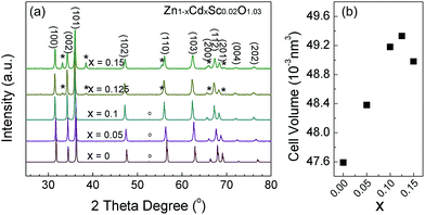 |
| | Fig. 1 (a) The XRD patterns of Zn1−xCdxSc0.02O1.03 (x = 0 to 0.15) samples. (b) Refined unit cell volume of the primary phase plotted as a function of Cd composition. | |
The XRD patterns of Zn0.9Cd0.1ScyO1+1.5y (y = 0 to 0.04) samples are presented in Fig. 2a and show that the main crystalline structure is still wurtzite (P63mc space group). For y = 0.02, 0.03 and 0.04, the secondary Sc2O3 phase that belongs to the I213 space group is indicated by weak peaks marked with ‘○’ (Fig. 2a). The unit cell volumes remain almost constant with very slight changes irrespective of y values (Fig. 2b). This is because the ionic radius of Cd2+ (0.078 nm, 4-fold coordination) is more similar to that of Sc3+ (0.075 nm, 6-fold coordination) than to that of Zn2+ (0.06 nm, 4-fold coordination). This confirmed that Sc substitution likely occurs at Cd sites. Table S2 in the ESI† presents the detailed parameters obtained from Rietveld refinement of the XRD patterns.
 |
| | Fig. 2 (a) The XRD patterns of Zn0.9Cd0.1ScyO1+1.5y (y = 0 to 0.04) samples. (b) Refined unit cell volume of the primary phase plotted as a function of Sc composition. | |
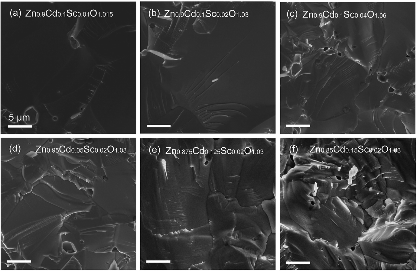
Representative SEM images of Zn1−xCdxSc0.02O1.03 (x = 0.05 to 0.15) and Zn0.9Cd0.1ScyO1+1.5y (y = 0.01 to 0.04) samples are shown in Fig. 3. A higher number of grain boundaries and smaller sized grains can be observed as the Sc concentration increases from 0.01 to 0.04 (Fig. 3a–c). Based on the XRD spectra presented in Fig. 3b and d, this trend can be attributed to the formation of the I213 secondary phase by excessive Sc. Cd addition promoted the sintering, and thus, the samples displayed fewer grain boundaries for a Cd concentration of 0.1 than for a Cd concentration of 0.05. Adding additional Cd degraded the microstructure by introducing more grain boundaries and pores at grain boundaries, as shown in Fig. 3e and f. This is because of the limited solubility of Cd in ZnO, which led to the loss of CdO during sintering above its melting temperature of 1120 K. The precipitation of the Fm3m secondary phases was also increased by excessive CdO.
 |
| | Fig. 3 SEM images of fractured surfaces for Zn0.9Cd0.1ScyO1+1.5y (y = 0.01 to 0.04) samples: (a) y = 0.01, (b) y = 0.2, (c) y = 0.04, and fractured surfaces for Zn1−xCdxSc0.02O1.03 (x = 0.05 to 0.15) samples: (d) x = 0.05, (e) x = 0.125, (f) x = 0.15. | |
To elucidate the precise distributions of Cd and Sc in the main ZnO matrix, STEM-EDS mapping was performed for Zn0.9Cd0.1Sc0.01O1.03. As shown in Fig. 4, Zn and Cd are alloyed well with each other in the grain interiors (Fig. 4c and d), which is consistent with the XRD results. Sc is not likely to be homogenously distributed. Instead, Sc segregates into separate particles (Fig. 4b), which is consistent with the observation of the I213 secondary phase from XRD spectra. However, Sc concentrations in the other areas are very low, indicating a low Sc solubility in CdO or ZnO.
 |
| | Fig. 4 STEM-EDS elemental mapping of a Zn0.9Cd0.1Sc0.01O1.03 sample: the dark field image in (a), the distribution of Sc in (b), the distribution of Zn in (c), and the distribution of Cd in (d). | |
Thermoelectric properties
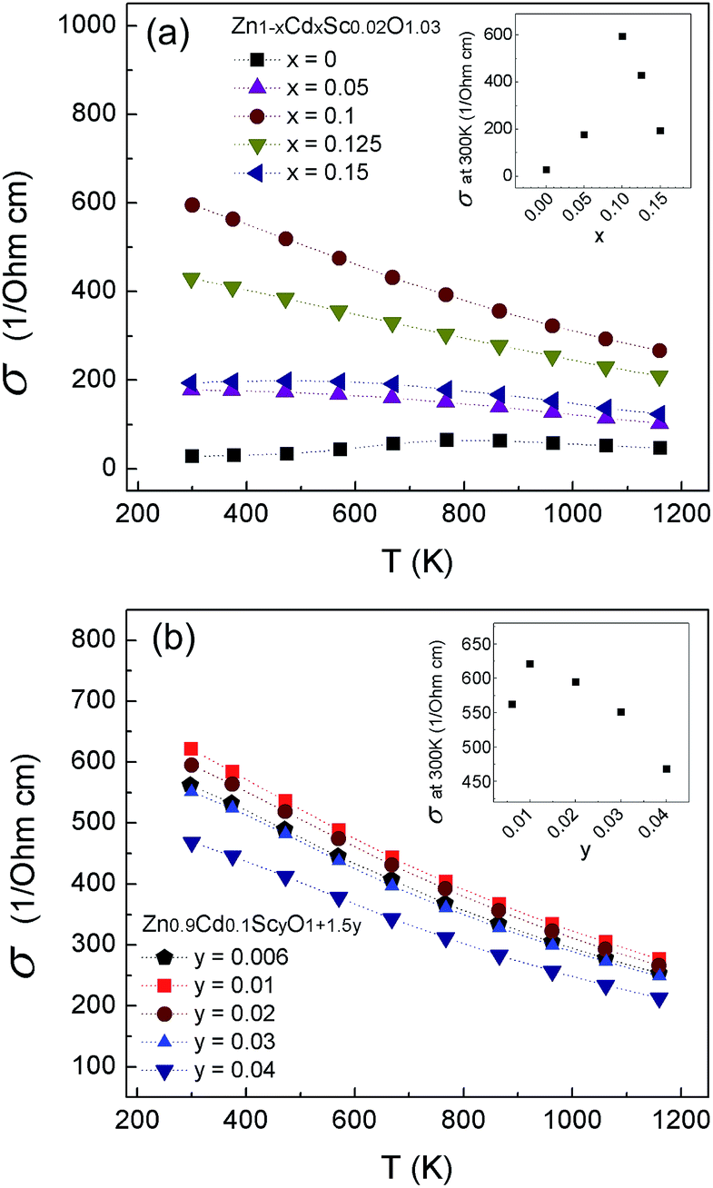
The electrical conductivities (σ) of the Zn1−xCdxSc0.02O1.03 (x = 0 to 0.15) samples are shown in Fig. 5a. The ZnSc0.02O1.03 sample exhibited the lowest conductivity with mixed conduction characteristics. As the Cd concentration increased, the corresponding σ values also increased. This is because according to XRD results, CdO addition provides substitution sites for Sc, so that the process expressed by| |  | (1) |
provides free carriers to the system, thereby increasing the conductivity. The highest conductivity was observed for the sample with x = 0.1, which exhibited metallic conduction behaviour. Further increasing the Cd content resulted in a decrease in σ (inset of Fig. 5a). This may be explained by the phase separation of CdO and the deterioration of the carrier mobility by increased grain boundary scattering and defect scattering. Such explanations were verified by the hall measurement results which are shown in Table 1 and will be discussed later. The influences of the Sc concentration on the electrical conductivity (σ) for the Zn0.9Cd0.1ScyO1+1.5y (y = 0.006 to 0.04) samples are shown in Fig. 5b. All the samples in this group show metallic conductivity. When y = 0.01, the conductivity is highest, which is comparable to that of the best Al doped ZnO bulk materials.35 As y increased beyond 0.01, the conductivity decreased (inset of Fig. 5b). This may be explained by the precipitation of the I213 secondary phase and the increased grain boundary scatterings.
 |
| | Fig. 5 Temperature dependence of the electrical conductivity σ for (a) Zn1−xCdxSc0.02O1.03 (x = 0 to 0.15) samples and (b) Zn0.9Cd0.1ScyO1+1.5y (y = 0.006 to 0.04) samples. | |
Table 1 Electrical transport properties at room temperature
| Sample |
σ (1/Ω cm−1) |
S (μV K−1) |
n (1019 cm−3) |
μ (cm2 V−1 S−1) |
D.O.S. effective mass (m*/me) |
| Zn1−xCdxSc0.02O1.03 |
x = 0 |
28.1 |
−194 |
0.24 |
71.6 |
0.19 |
|
x = 0.05 |
177 |
−60.1 |
3.52 |
31.4 |
0.33 |
|
x = 0.1 |
595 |
−70.6 |
5.61 |
66.2 |
0.53 |
|
x = 0.125 |
429 |
−72.5 |
5.99 |
44.8 |
0.56 |
|
x = 0.15 |
193 |
−58.1 |
5.48 |
22.1 |
0.42 |
| Zn0.9Cd0.1ScyO1+1.5y |
y = 0.01 |
621 |
−73.9 |
5.84 |
67 |
0.57 |
|
y = 0.02 |
595 |
−70.6 |
5.61 |
66.2 |
0.53 |
|
y = 0.03 |
552 |
−76.5 |
6.02 |
57.2 |
0.59 |
|
y = 0.04 |
469 |
−84.1 |
4.71 |
62 |
0.56 |
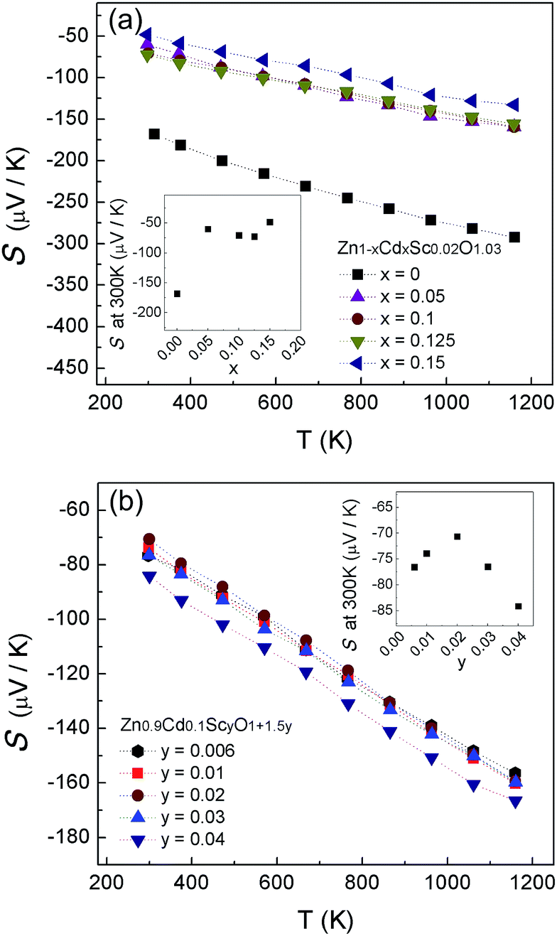
Fig. 6 shows the temperature dependence of the samples' Seebeck coefficients (S). Their negative S values indicated n-type conduction. Additionally, the monolithically increasing absolute S values with increasing temperature suggested the thermal excitation of electrons and the negligible contribution from bipolar conduction. Fig. 6a shows that the ZnSc0.02O1.03 sample had the highest |S| because it had the lowest carrier concentration n (Table 1). The addition of Cd severely lowered the |S| by significantly increasing n. However, increasing the effective mass m*/me had a positive effect, preventing |S| from becoming too low. When x = 0.1, |S| is still much higher than that of our previous AZO sample26 which has a similar n. Fig. 7b shows the temperature dependence of the Seebeck coefficients, S, of the Zn0.9Cd0.1ScyO1+1.5y (y = 0.006 to 0.04) samples. The |S| values for all samples were found to be very similar. The Zn0.9Cd0.1Sc0.02O1.03 sample had a slightly higher |S| value than the other compositions. The inset of Fig. 7b shows the plot of S at room temperature vs. y for the Zn0.9Cd0.1ScyO1+1.5y.
 |
| | Fig. 6 Temperature dependence of the Seebeck coefficient S for (a) Zn1−xCdxSc0.02O1.03 (x = 0 to 0.15) samples and (b) Zn0.9Cd0.1ScyO1+1.5y (y = 0.006 to 0.04) samples. | |
 |
| | Fig. 7 Room temperature Seebeck coefficient S plotted as a function of carrier concentration n for (a) Zn0.9Cd0.1ScyO1+1.5y (y = 0.01 to 0.04) samples, and (b) Zn1−xCdxSc0.02O1.03 (x = 0 to 0.15) samples. The solid colored lines represent the calculated values based on (a) scattering mechanisms with m*/me = 0.59 and (b) effective mass with λ = 0. | |
A room-temperature Hall measurement was conducted to determine the carrier concentration (n), and the results are presented in Table 1 together with the results for other electrical transport properties. The effective mass (m*/me) was obtained according to the Pisarenko relation, as discussed previously.26 The addition of Cd increased n to the order of 1019 cm−3 without severely decreasing μ. For x = 0.1, μ was maintained at 66.2 cm2 V−1 S−1, which is comparable or higher than the value obtained for the AZO samples.24–26 In contrast, m*/me was notably increased by increasing Cd from 0.19 for ZnSc0.02O1.03 to 0.53 for Zn0.9Cd0.1Sc0.02O1.03, and the latter's value exceeded that of ZnAl0.02O1.03 (∼0.4).26 However, the addition of excessive Cd, e.g., x = 0.15, resulted in a reverse effect, lowering the n, μ, and m*/me values, which is not desirable. Changing the Sc concentration from 0.01 to 0.04 had a much smaller effect on the transport properties than changing the Cd content. n and μ were found to be relatively stable with only minor fluctuations. Using the n and m*/me values shown in Table 1, a simple parabolic band model1 can be applied to describe the carrier density and Seebeck coefficient:
| |  | (2) |
| |  | (3) |
| |  | (4) |
where
Fλ(
ξ) is the Fermi integral and
ξ is the reduced electrochemical potential.
λ is a scattering parameter which takes the value 0 for acoustic phonon scattering, 1 for optical phonon scattering, and 2 for ionized impurity scattering.
1Fig. 7 shows
S as a function of
n at room temperature. In
Fig. 7a, the
S values for Zn
0.9Cd
0.1Sc
yO
1+1.5y (
y = 0.01 to 0.04) samples correspond very well to
λ = 0, indicating that acoustic phonon scattering is the dominant scattering mechanism. In
Fig. 7b, the three lines correspond to the three different
m* values obtained assuming that acoustic phonon scattering is the dominant scattering mechanism. A clear increase of
m* with increasing
x can be observed. Given that their
μ values are comparable, according to the band theory,
27 it is reasonable to suggest that the increase of
m* arises from the convergence of the conduction bands in Zn
1−xCd
xSc
0.02O
1.03 (
x = 0.05 to 0.15). However, further investigations are needed to confirm this hypothesis.
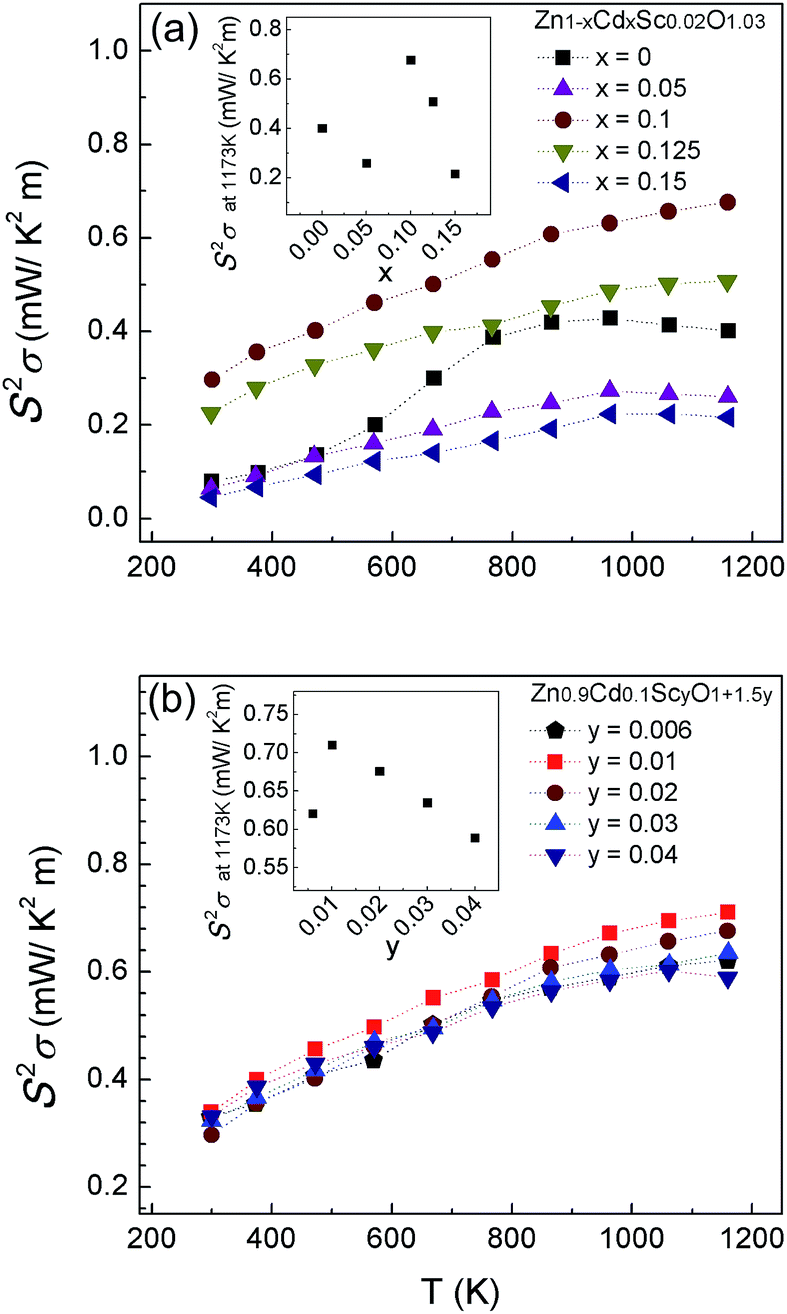
Fig. 8 shows the power factor (S2σ) of the samples. For the Zn1−xCdxSc0.02O1.03 (x = 0 to 0.15) samples shown in Fig. 8a, the highest S2σ values were obtained for x = 0.1 because of the well-maintained μ and adequately increased n and m*. Further increasing x decreased S2σ. For the Zn0.9Cd0.1ScyO1+1.5y (y = 0.006 to 0.04) samples, the change in S2σ with changing y was not as pronounced as that with changing x. Among the tested values, the highest power factor of ∼ 7.1 × 10⁻⁴ W m−1 K−2 at 1173 K was achieved for y = 0.01; this value is comparable to that of the conventional AZO.26
 |
| | Fig. 8 Temperature dependence of the power factor S2σ for (a) Zn1−xCdxSc0.02O1.03 (x = 0 to 0.15) samples, and (b) Zn0.9Cd0.1ScyO1+1.5y (y = 0.006 to 0.04) samples. | |
Fig. 9a shows the total thermal conductivity as a function of temperature for the Zn1−xCdxSc0.02O1.03 (x = 0 to 0.15) samples. For x = 0, ZnSc0.02O1.03 shows a high thermal conductivity similar to those of pure ZnO and AZO.35 The addition of Cd effectively reduced the thermal conductivity by alloy scattering. The Zn0.9Cd0.1Sc0.02O1.03 sample showed 7-fold lower thermal conductivity than the ZnSc0.02O1.03 sample. The decrease in the thermal conductivity with increasing Cd concentration continued to a minimum of ∼2.5 W m−1 K−1 at 1173 K (x = 0.125). Further increasing the Cd content had a reverse effect on the thermal conductivity values, presumably because of phase separation. The small κ values obtained for the Zn0.875Cd0.125Sc0.02O1.03 sample are comparable to or even smaller than those previously reported for the AZO nanocomposites (κ values between 2 and 3.5 W m−1 K−1 at 1173 K).24–26 The lattice contribution κL to the total κ was estimated using a reduced Lorenz number of 1.8 × 10⁻⁸ WΩK−2. The extracted κL values are shown in Fig. 9b. The values of κL are somewhat similar to the values of κ, indicating that the lattice component dominates the thermal conductivity for all the samples. The Debye–Callaway model36–39 was used to calculate the lattice thermal conductivity as follows:
| |  | (5) |
where
kB is the Boltzmann constant,
v is the speed of sound,
ħ is the reduced Planck's constant,
x is the normalized frequency
ħω/
kBT,
T is the absolute temperature, and
θ is the Debye temperature.
τc is the combined relaxation time calculated using Mathieson's rule as follows:
| | | τc−1 = τpad−1 + τN−1 + τB−1 | (6) |
where
τc is composed of alloy point defect scattering
τpad, normal phonon–phonon scattering
τN, and boundary scattering
τB. The relaxation time for these scattering mechanisms is calculated from the following relations:
where
A,
B,
α and
β are the scattering strength-related parameters,
ω is the phonon frequency, and
L is the average grain size values. The parameters used for the calculations are listed in Table S3 in the ESI.
† The calculated results are shown as solid lines in
Fig. 9b. The calculations indicated that the reduction of the thermal conductivity was mainly caused by point defect scattering or alloy scattering, indicating that adding CdO results in oxide alloys with ZnO. The grain size also influences the reduction of the thermal conductivity, but its influence is quite small compared to that of alloy scattering.
 |
| | Fig. 9 Temperature dependence of (a) the total thermal conductivity κ and (b) the lattice thermal conductivity κL for Zn1−xCdxSc0.02O1.03 (x = 0 to 0.15) samples. The solid lines in (b) represent values calculated using a Debye–Callaway model. | |
Fig. 10a shows the thermal conductivity as a function of temperature for the Zn0.9Cd0.1ScyO1+1.5y (y = 0.006 to 0.04) samples. Varying the Sc concentration in this range exerted a small effect on the thermal conductivity. All samples in this group have comparable thermal conductivities. As the Sc concentration increased, the thermal conductivity slightly decreased, and the lowest κ value was obtained for y = 0.04. The lattice contribution κL to the total κ was estimated and is shown in Fig. 11b. The values of κL remain similar to the values of the total conductivity. The calculated values are shown as solid lines in the figure.
 |
| | Fig. 10 Temperature dependence of (a) the total thermal conductivity κ and (b) the lattice thermal conductivity κL for Zn0.9Cd0.1ScyO1+1.5y (y = 0.006 to 0.04) samples. The solid lines in (b) represent values calculated using a Debye–Callaway model. | |
 |
| | Fig. 11 The phonon MFP vs. normalized phonon frequency (ħω/kBT) at (a) 300 K and (b) 1173 K according to the Debye–Callaway model. | |
To elucidate the mechanism of the alloy scattering based reduction of lattice thermal conductivity, the phonon mean free path (MFP) was plotted against the normalized phonon frequency (ħω/kBT) according to the Debye–Callaway model, as shown in Fig. 10. At 300 K, most of the phonon spectrum, especially in the lower-frequency region, was reduced significantly as x increased from 0 to 0.1, providing a good explanation for the 7-fold-smaller thermal conductivity obtained for the Zn0.9Cd0.1Sc0.02O1.03 sample compared to that of the ZnSc0.02O1.03 sample (Fig. 11a). At 1173 K, the effect of alloy scattering remains quite pronounced because of the depression of the phonon spectrum in the intermediate- and high-frequency regions (Fig. 11b). Additionally, density functional theory (DFT) calculations of phonon density of states (DOS) spectra were performed for these samples. A clear red shift relative to ZnO and the occurrence of low-energy phonons were observed for Zn0.875Cd0.125O. These results revealed the signature of phonon glass formed by alloying Cd into ZnO (Fig. S1 in the ESI†).
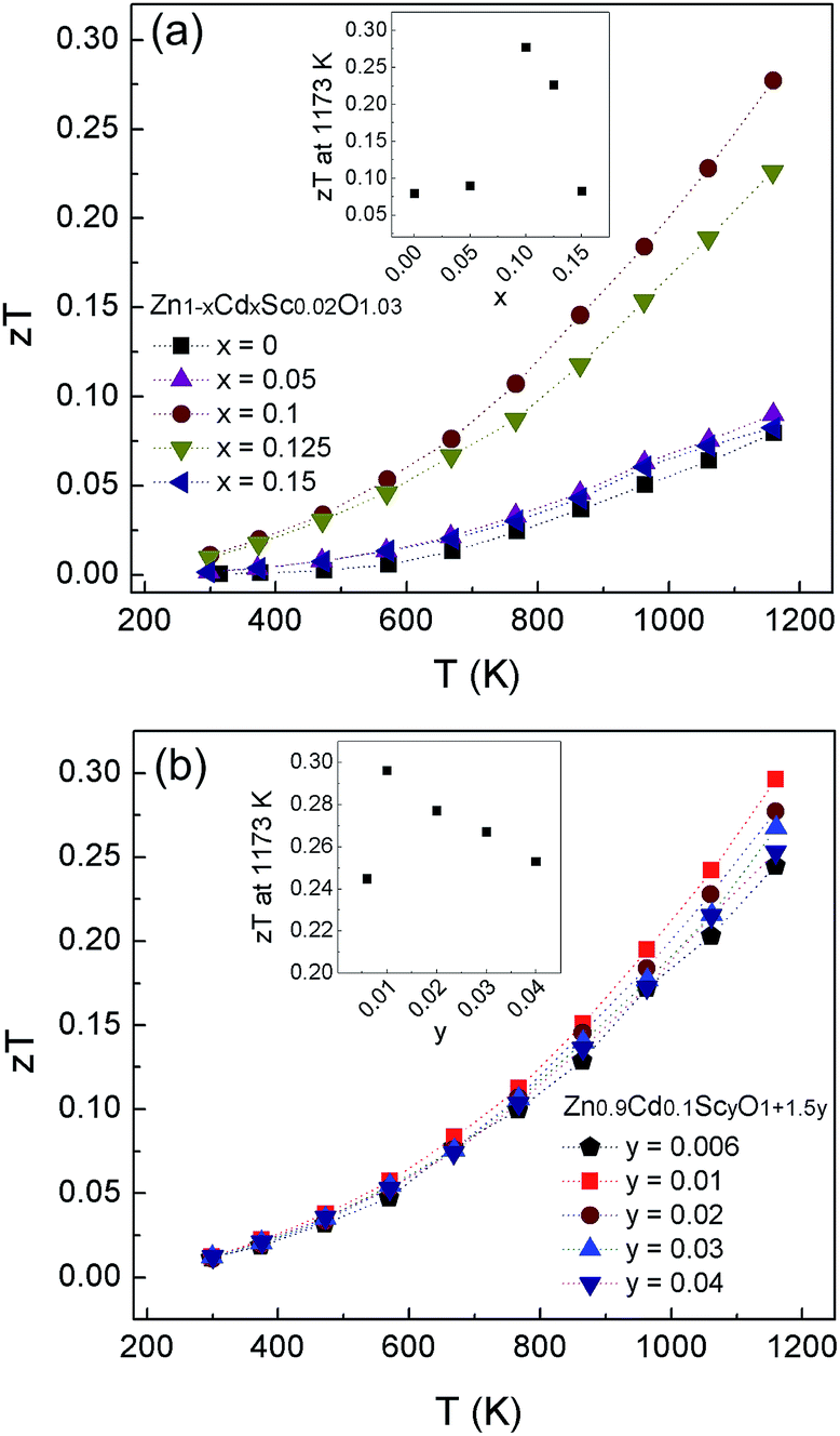
The values for the ZT figure of merit are shown in Fig. 12. When x = 0, the peak ZT value at 1173 K for the ZnSc0.02O1.03 sample is only 0.075, even lower than that previously obtained for the AZO;40 when x = 0.1, the peak ZT value at 1173 K for Zn0.9Cd0.1Sc0.02O1.03 was increased to 0.28, corresponding to an improvement by a factor of 2.73. Further increasing the Cd concentration only decreased the obtained ZT values. Clearly, adding Cd significantly influences the ZT. In Fig. 12b, the ZT values for Zn0.9Cd0.1ScyO1+1.5y (y = 0.006 to 0.04) samples are quite similar. Despite the error bar for the ZT values (∼30%), Zn0.9Cd0.1Sc0.1O1.15 achieved the highest peak ZT value: 0.3 at 1173 K. Comparing the ZT of Zn0.9Cd0.1Sc0.1O1.15 to our previous results for AZO26,40 and the state-of-the-art AZO from literature results24,25,35,41 shows that Zn0.9Cd0.1Sc0.01O has one of the highest currently known ZT values over a range of temperatures among ZnO based TE materials, e.g., its ZT value of 0.012 at 300 K is over 1 order of magnitude higher than that (0.0013) obtained for the state-of-the-art nanostructured AZO.24,25 Thus, this material is a good candidate for improving the overall conversion efficiencies in oxide TE modules.
 |
| | Fig. 12 Temperature dependence of the figure of merit ZT for (a) Zn1−xCdxSc0.02O1.03 (x = 0 to 0.15) samples and (b) Zn0.9Cd0.1ScyO1+1.5y (y = 0.006 to 0.04) samples. | |
Engineering power factor and figure of merit ZT
An engineering power factor (PF)eng and a dimensionless engineering figure of merit (ZT)eng were defined by Ren et al. as a function of the temperature difference between the cold and hot sides to reliably predict the output power and practical conversion efficiency, respectively.42 These factors are defined by formulas with cumulative temperature-dependent properties and are expressed as follows:
where TH is the hot side temperature, Tc is the cold side temperature, and ΔT is the temperature difference between the cold and hot sides. The as-defined (PF)eng and (ZT)eng can reliably predict the output power and practical conversion efficiency, respectively, thereby preventing the reporting of unrealistic efficiency values using average ZT values and complex numerical simulations. Therefore, the (PF)eng and (ZT)eng for the new Zn0.9Cd0.1Sc0.1O1.15 material were calculated and compared with those for the other state-of-the-art AZO samples, as shown in Fig. 13. Zn0.9Cd0.1Sc0.1O1.15 shows the highest (PF)eng because of its superior electrical transport properties relative to the AZO, although the bulk AZO40 shows a higher peak PF at 1173 K than the new materials. Compared to the other AZO nanocomposites, this improvement was even more substantial. When TH = 1173 K, the (PF)eng of Zn0.9Cd0.1Sc0.1O1.15 was ∼0.5 W m−1 K−1, whereas that of the AZO nanocomposite was ∼0.05–0.15 W m−1 K−1. Fig. 13b shows the (ZT)eng of these samples as a function of TH. The AZO nanocomposite exhibited higher (ZT)eng than the AZO bulk samples. When TH = 1173 K, the (ZT)eng of the AZO nanocomposite was higher than that of the AZO bulk by a factor of ∼2, whereas the new Zn0.9Cd0.1Sc0.1O1.15 showed ∼10 times-higher (ZT)eng than the AZO bulk, suggesting that the new material has a significantly enhanced practical conversion efficiency compared to the conventional AZO materials.
 |
| | Fig. 13 Comparison of Zn0.9Cd0.1Sc0.1O1.15 with other AZO materials reported in the literature24,25,40 in terms of (a) the engineering power factor (PF)eng and (b) the engineering figure of merit (ZT)eng, as a function of hot side temperature TH. The cold side temperature Tc is 300 K. | |
High temperature stability in air
One of the most striking advantages of this newly developed material is its stability in air. For a long time, ZnO based materials, such as AZO, have suffered from electrical conductivity degradation in air at high temperatures. Such degradation is related to the elimination of intrinsic electron donor defects within ZnO, such as oxygen vacancies VO, zinc interstitials, Zni, and zinc antisites, Zno. The formation of these point defects follows these general reaction equations:43| |  | (11) |
| |  | (12) |
| |  | (13) |
where δ, β, λ = 1 or 2, and the equilibrium constants of reactions (11)–(13) can be obtained using the mass action law, as expressed by the following equations:| |  | (14) |
| |  | (15) |
| |  | (16) |
where PO2 represents the partial pressure of oxygen in the system. From these equations we can see that the probabilities of forming oxygen vacancies, zinc interstitials, and zinc antisite defects are all related to the partial pressure of oxygen in the system. The charge carrier concentrations are also directly related to these reactions. Moreover, the dopant impurities, for example, AlZn˙, Zni˙, also undergo a reaction with oxygen by:| | | 2AlZn˙ + Zni˙ + 3e′ + 2O2 → ZnAl2O4 | (17) |
in which ZnAl2O4 is a non-conducting spinel phase,40 the same as ZnGa2O4 in Ga-doped ZnO. According to previous investigations,44 Zn antisites and Zn interstitials are the main source of free electrons in doped ZnO. However, when heated at an elevated temperature with excessive oxygen, Zn antisites and Zn interstitials undergo chemical reactions and form insulating secondary phases such as ZnA2O4 and ZnGa2O4. Therefore the Ga and Al-doped ZnO work usually at a semi-stable state with defects, for example, sintered in nitrogen. After curing with oxygen at high temperature, their carrier density would dramatically decrease and therefore they are not suitable for high temperature thermoelectrics in air.
In contrast, the new material bypasses the problem by introducing Cd and Sc dopants, a majority of the donors are from the Sc replacing Cd, ScCd˙, and there are no irreversible chemical reactions that will lead to the formation of insulating phases, as previously discussed in eqn (1). To verify its stability, an in situ measurement of the electrical conductivity σ in air was performed for the new Zn0.9Cd0.1Sc0.02O1.03 and the conventional Zn0.98Al0.02O1.03 samples from our previous work40 to compare their thermal stability, as shown in Fig. 14. Both samples were treated with two heating and cooling cycles up to 1073 K in air over approximately 48 hours. Zn0.9Cd0.1Sc0.02O1.03 showed stable σ compared to Zn0.98Al0.02O1.03, whereas the latter's σ decreased by more than 1 order of magnitude after the cycles, consistent with the observations of Schäuble et al.45.
 |
| | Fig. 14 Electrical conductivity σ of Zn0.9Cd0.1Sc0.02O1.03 and Zn0.98Al0.02O1.03 samples40 during heating and cooling cycles in air. | |
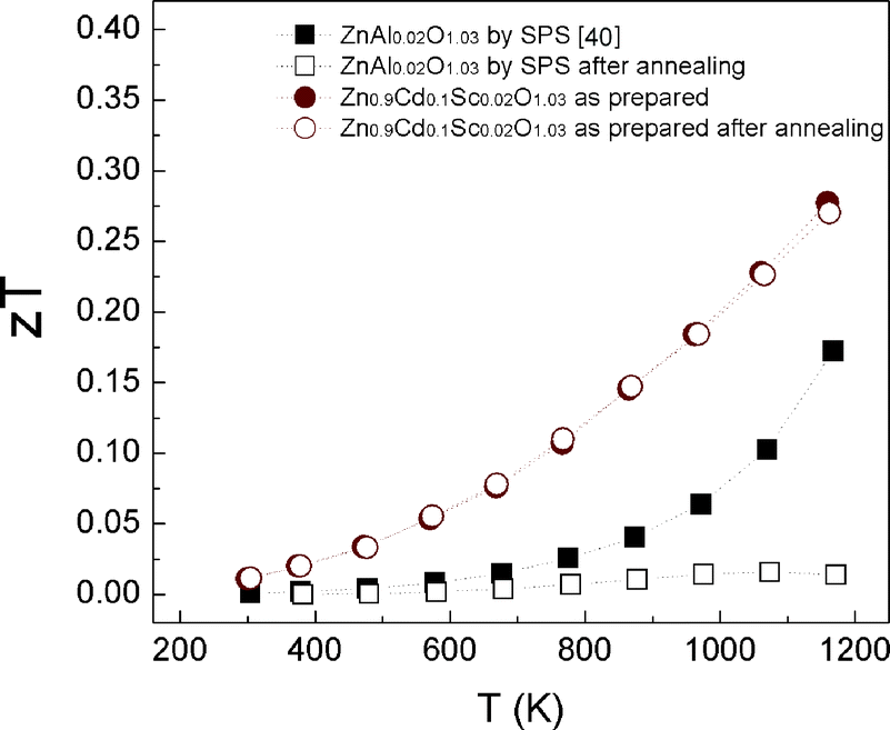
The TE long-term stability was also tested by annealing the samples in air at 1073 K for 72 h in a muffle furnace with the TE properties of ZnAl0.2O1.03 and Zn0.9Cd0.1Sc0.02O1.03 measured before and after the annealing. The figure of merit ZT before and after annealing is shown in Fig. 15. A slight degradation of ZT ∼ 5% occurred in the Zn0.9Cd0.1Sc0.02O1.03 sample after 72 h of annealing in air despite the errors, whereas the Zn0.98Al0.02O1.03 sample showed extremely large degradation (up to ∼90%). Changes in the electrical transport properties constituted the major reason for the change in the ZT, because the change in the lattice thermal conductivity was negligible. The TE properties of the samples, both before and after the annealing, are concluded in Fig. S2 in the ESI†. The degradation of ZnAl0.02O1.03 is mainly attributable to the elimination of donor defects such as zinc interstitials and oxygen vacancies, and can be simply observed by the changes in the samples' colour. In Fig. 16a and c, the ZnAl0.02O1.03 sample appeared dark after SPS in a vacuum, but after annealing in air at 1073 K for 72 h, the segment turned light yellow, indicating a significant change in its electrical properties. In contrast, in Fig. 16b and d, the Zn0.9Cd0.1Sc0.02O1.03 sample sintered in air retained its dark greenish colour after annealing in air at 1073 K for 72 h. Nevertheless, the stability of the material under working conditions in a large temperature gradient (>500 K) in air should be further investigated.
 |
| | Fig. 15 Temperature dependence of the figure-of-merit ZT for Zn0.9Cd0.1Sc0.02O1.03 and Zn0.98Al0.02O1.03 samples40 before and after annealing for 72 h at 1073 K in air. | |
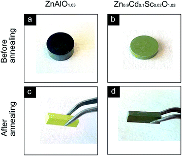 |
| | Fig. 16 Photographs of (a) a bulk pellet of ZnAl0.02O1.03 sintered by spark plasma sintering in a vacuum, (b) a bulk pellet of Zn0.9Cd0.1Sc0.02O1.03 sintered in air, (c) a cuboid segment of ZnAl0.02O1.03 after annealing in air at 1073 K for 72 h, (d) a cuboid segment of Zn0.9Cd0.1Sc0.02O1.03 after annealing in air at 1073 K for 72 h. | |
Conclusions
The TE properties of newly developed Sc-doped ZnCdO materials were systematically investigated. The Zn0.9Cd0.1Sc0.01O1.03 sample showed the highest ZT (∼0.3 at 1173 K and ∼0.24 at 1073 K) and a good engineering ZT that was significantly higher than those of the nanostructured AZO materials. These superior ZT values can be attributed to the alloying of CdO with ZnO, which significantly reduced the lattice thermal conductivity. Meanwhile, the alloying of CdO increased the DOS effective mass without decreasing the carrier mobility. After tuning the carrier concentration, a large power factor of ∼7.1 × 10⁻⁴ W m−1 K−1 was obtained. Meanwhile, Sc-doped ZnCdO is robust in air at high temperatures up to 1073 K for 72 h, and its TE performance is retained after heating and cooling cycles in air. In contrast, other ZnO based TE materials, such as AZO, experience rapid degradation of their TE performances. Overall, the Sc-doped ZnCdO material represents a new and promising n-type material with superior properties for high-temperature TE applications.
Acknowledgements
The authors would like to thank the Department of Energy Conversion and Storage, Technical University of Denmark for generously supporting this research work. This research work was sponsored by the Programme Commission on Energy and Environment (EnMi) which is a part of the Danish Council for Strategic Research (Contract No. 10-093971), and the authors would also like to thank the European Union's Seventh Programme for research, technological development and demonstration (grant agreement No. 604647) for sponsoring the NanoCaTe research project.
Notes and references
- D. M. Rowe, New York, 1995, 16, 1251–1256 Search PubMed.
- G. J. Snyder and E. S. Toberer, Nat. Mater., 2008, 7, 105–114 CrossRef CAS PubMed.
- Y. Gelbstein, Z. Dashevsky and M. P. Dariel, Phys. B, 2007, 396, 16–21 CrossRef CAS.
- Y. Gelbstein, J. Davidow, S. N. Girard, D. Y. Chung and M. Kanatzidis, Adv. Energy Mater., 2013, 3, 815–820 CrossRef CAS.
- K. Kirievsky, Y. Gelbstein and D. Fuks, J. Solid State Chem., 2013, 203, 247–254 CrossRef CAS.
- Y. Gelbstein, N. Tal, A. Yarmek, Y. Rosenberg, M. P. Dariel, S. Ouardi, B. Balke, C. Felser and M. Köhne, J. Mater. Res., 2011, 26, 1919–1924 CrossRef CAS.
- A. Pokhrel, Z. P. Degregorio, J. M. Higgins, S. N. Girard and S. Jin, Chem. Mater., 2013, 25, 632–638 CrossRef CAS.
- Y. Sadia, L. Dinnerman and Y. Gelbstein, J. Electron. Mater., 2013, 42, 1926–1931 CrossRef CAS.
- K. Koumoto, Y. Wang, R. Zhang, A. Kosuga and R. Funahashi, Annu. Rev. Mater. Res., 2010, 40, 363–394 CrossRef CAS.
- Y. Wang, Y. Sui, F. Li, L. Xu, X. Wang, W. Su and X. Liu, Nano Energy, 2012, 1, 456–465 CrossRef CAS.
- N. Van Nong, N. Pryds, S. Linderoth and M. Ohtaki, Adv. Mater., 2011, 23, 2484–2490 CrossRef CAS PubMed.
- N. Wang, H. Li, Y. Ba, Y. Wang, C. Wan, K. Fujinami and K. Koumoto, J. Electron. Mater., 2010, 39, 1777–1781 CrossRef CAS.
- H. Ohta, S. Kim, Y. Mune, T. Mizoguchi, K. Nomura, S. Ohta, T. Nomura, Y. Nakanishi, Y. Ikuhara, M. Hirano, H. Hosono and K. Koumoto, Nat. Mater., 2007, 6, 129–134 CrossRef CAS PubMed.
- M. Ohtaki, T. Tsubota, K. Eguchi and H. Arai, J. Appl. Phys., 1996, 79, 1816 CrossRef CAS.
- M. Ohtaki, K. Araki and K. Yamamoto, J. Electron. Mater., 2009, 38, 1234–1238 CrossRef CAS.
- L. T. Hung, N. Van Nong, L. Han, D. Le Minh, K. a. Borup, B. B. Iversen, N. Pryds and S. Linderoth, J. Mater. Sci., 2012, 48, 2817–2822 CrossRef.
- D. Flahaut, T. Mihara, R. Funahashi, N. Nabeshima, K. Lee, H. Ohta and K. Koumoto, J. Appl. Phys., 2006, 100, 084911 CrossRef.
- S.-M. Choi, C.-H. Lim and W.-S. Seo, J. Electron. Mater., 2010, 40, 551–556 CrossRef.
- L. Bocher, M. H. Aguirre, D. Logvinovich, A. Shkabko, R. Robert, M. Trottmann and A. Weidenkaff, Inorg. Chem., 2008, 47, 8077–8085 CrossRef CAS PubMed.
- T. Minami, T. Miyata and T. Yamamoto, J. Vac. Sci. Technol., A, 1999, 17, 1822 CAS.
- Y. Wang, Y. Sui, H. Fan, X. Wang, Y. Su, W. Su and X. Liu, Chem. Mater., 2009, 21, 4653–4660 CrossRef CAS.
- K. Koumoto, R. Funahashi, E. Guilmeau, Y. Miyazaki, A. Weidenkaff, Y. Wang and C. Wan, J. Am. Ceram. Soc., 2013, 96, 1–23 CrossRef CAS.
- Y. Kinemuchi, H. Nakano, M. Mikami, K. Kobayashi, K. Watari and Y. Hotta, J. Appl. Phys., 2010, 108, 053721 CrossRef.
- P. Jood, R. J. Mehta, Y. Zhang, G. Peleckis, X. Wang, R. W. Siegel, T. Borca-Tasciuc, S. X. Dou and G. Ramanath, Nano Lett., 2011, 11, 4337–4342 CrossRef CAS PubMed.
- W. H. Nam, Y. S. Lim, S.-M. Choi, W.-S. Seo and J. Y. Lee, J. Mater. Chem., 2012, 22, 14633 RSC.
- L. Han, N. Van Nong, W. Zhang, L. T. Hung, T. Holgate, K. Tashiro, M. Ohtaki, N. Pryds and S. Linderoth, RSC Adv., 2014, 4, 12353 RSC.
- Y. Pei, X. Shi, A. LaLonde, H. Wang, L. Chen and G. J. Snyder, Nature, 2011, 473, 66–69 CrossRef CAS PubMed.
- L. D. Zhao, H. J. Wu, S. Q. Hao, C. I. Wu, X. Y. Zhou, K. Biswas, J. Q. He, T. P. Hogan, C. Uher, C. Wolverton, V. P. Dravid and M. G. Kanatzidis, Energy Environ. Sci., 2013, 6, 3346–3355 CAS.
- Y. Pei, H. Wang and G. J. Snyder, Adv. Mater., 2012, 24, 6125–6135 CrossRef CAS PubMed.
- Y. Pei, N. a. Heinz and G. J. Snyder, J. Mater. Chem., 2011, 21, 18256 RSC.
- Y. Zhu, G. Chen, H. Ye, A. Walsh, C. Moon and S.-H. Wei, Phys. Rev. B: Condens. Matter Mater. Phys., 2008, 77, 245209 CrossRef.
-
V. Venkatachalapathy, PhD Thesis, University of Oslo, 2011 Search PubMed.
- V. Venkatachalapathy, A. Galeckas, M. Trunk, T. Zhang, A. Azarov and A. Y. Kuznetsov, Phys. Rev. B: Condens. Matter Mater. Phys., 2011, 83, 125315 CrossRef.
- K. P. Ong, D. J. Singh and P. Wu, Phys. Rev. B: Condens. Matter Mater. Phys., 2011, 83, 115110 CrossRef.
- T. Tsubota, M. Ohtaki, K. Eguchi and H. Arai, J. Mater. Chem., 1997, 7, 85–90 RSC.
- J. Callaway, Phys. Rev., 1959, 113, 1046–1051 CrossRef CAS.
- D. Cahill, S. Watson and R. Pohl, Phys. Rev. B: Condens. Matter Mater. Phys., 1992, 46, 6131–6140 CrossRef CAS.
- A. Majumdar, J. Heat Transfer, 1993, 115, 7 CrossRef.
- K. S. Dubey and R. H. Misho, Phys. Stat. Sol., 1977, 84, 69–81 CrossRef CAS.
- L. Han, N. Van Nong, L. T. Hung, T. Holgate, N. Pryds, M. Ohtaki and S. Linderoth, J. Alloys Compd., 2013, 555, 291–296 CrossRef CAS.
- M. Søndergaard, E. D. Bøjesen, K. A. Borup, S. Christensen, M. Christensen and B. B. Iversen, Acta Mater., 2013, 61, 3314–3323 CrossRef.
- H. S. Kim, W. Liu, G. Chen, C.-W. Chu and Z. Ren, Proc. Natl. Acad. Sci., 2015, 112, 8205–8210 CrossRef CAS PubMed.
- A. Janotti and C. G. Van de Walle, Rep. Prog. Phys., 2009, 72, 126501 CrossRef.
- U. Özgür, Y. I. Alivov, C. Liu, a. Teke, M. a. Reshchikov, S. Doğan, V. Avrutin, S.-J. Cho and H. Morkoç, J. Appl. Phys., 2005, 98, 041301 CrossRef.
- N. Vogel-Schäuble, Y. E. Romanyuk, S. Yoon, K. J. Saji, S. Populoh, S. Pokrant, M. H. Aguirre and A. Weidenkaff, Thin Solid Films, 2012, 520, 6869–6875 CrossRef.
Footnote |
| † Electronic supplementary information (ESI) available: Calculated results from Rietveld refinements of XRD spectra, parameters used for the Callaway model, calculated phonon density of states by DFT calculation, and supplement TE properties. See DOI: 10.1039/c6ta03126a |
|
| This journal is © The Royal Society of Chemistry 2016 |
Click here to see how this site uses Cookies. View our privacy policy here. 
 Open Access Article
 This Open Access Article is licensed under a Creative Commons Attribution-Non Commercial 3.0 Unported Licence