
 Open Access Article
 This Open Access Article is licensed under a
 Creative Commons Attribution 3.0 Unported Licence
Metal-substrate-supported tungsten-oxide nanoarrays via porous-alumina-assisted anodization: from nanocolumns to nanocapsules and nanotubes†
Alexander
Mozalev
*a,
Maria
Bendova
a,
Francesc
Gispert-Guirado
b,
Zdenek
Pytlicek
a and
Eduard
Llobet
b
aCEITEC – Central European Institute of Technology, Brno University of Technology, Technicka 10, 61600 Brno, Czech Republic. E-mail: alexander.mozalev@ceitec.vutbr.cz
bMINOS-EMaS, University Rovira i Virgili, Av. Paisos Catalans 26, 43007 Tarragona, Spain
First published on 20th April 2016
Abstract
An array of highly aligned tungsten-oxide (TO) nanorods, ∼80 nm wide, up to 900 nm long, spatially separated at their bottoms by tungsten metal on a substrate is synthesized via the self-localized anodization of aluminum followed by the porous-alumina-assisted re-anodization of tungsten in a sputter-deposited Al/W bilayer. Moreover, the pore-directed TO nanocapsules may grow, which can be electrochemically top-opened in alumina nanopores and transformed to TO nanotubes, representing unique architectures built up on tungsten substrates to date. The as-grown nanorods are composed of amorphous WO3 mixed with minor amounts of WO2 and Al2O3 in the outer layer and oxide–hydroxide compound (WO3·nH2O) with aluminum tungstate (2Al2O3·5WO3), mainly present inside the rods. Once the growing oxide fills up the pores, it comes out as an array of exotic protuberances of highly hydrated TO, with no analogues among the other valve-metal oxides. Vacuum or air annealing at 550 °C increases the portion of non-stoichiometric oxides ‘doped’ with OH-groups and gives monoclinic WO2.9 or a mixture of WO3 and WO2.9 nanocrystalline phases, respectively. The nanorods show n-type semiconductor behavior when examined by Mott–Schottky analysis, with a high carrier density of 7 × 10¹⁹ or 3 × 1019 cm−3 for the air- or vacuum-annealed samples, associated with a charge depletion layer of about 8 or 10 nm, respectively. A model for the growth of the metal-substrate-separated TO nanocapsules and tubes is proposed and experimentally justified. The findings suggest that the new TO nanoarrays with well-defined nano-channels for carriers may form the basic elements for photoanodes or emerging 3-D micro- and nano-sensors.
1 Introduction
Tungsten oxide (TO) has become one of the most investigated functional metal oxides impacting many research fields. TO is useful for a variety of commercial and potential applications, including electro- and photo-chromic, thermo- and ferro-electric, photocatalytic, chemical, and gas-sensing devices, and, more recently, has been employed in the development of dye-sensitized solar cells, optical data storage devices, field-emission cathodes, and high-Tc superconductors.1Despite the large number of potential applications and useful properties, the well-controlled preparation of TO films with reproducible chemical composition, morphology, structure, and engineering performance remains a challenge.1–3 Nowadays, functionalization of TOs is based on increasing the surface-to-volume ratio, which intensifies chemical and physical interactions, and making the films regularly micro- and nano-structured and ‘decorated’ with some other nanomaterials, which significantly influence charge transport, electronic and optical properties of the material and may offer unique characteristics not found in the bulk form.4–7 Vapor-phase synthesis (sputtering, thermal evaporation, pulsed laser deposition, arc-discharge deposition, and chemical vapor deposition), liquid-phase synthesis (sol–gel, hydrothermal, and electrodeposition), and combined techniques have been recently developed for nanostructuring tungsten oxides.1 Since the first reports by Mukherjee et al.,8 nanoporous TO films grown via direct anodizing of tungsten have been the subject of several studies.9–12 Despite the most recent advances in this approach,13 the anodic TO films grow as sponge-like nanoporous layers with an irregular morphology, platelet crystals,14 or nanoparticles on a substrate.15
An alternative electrochemical approach based on porous-anodic-alumina16 (PAA)-assisted anodization17 of a layer of tungsten18 has generated arrays of TO nanodots and nanocolumns self-organized on a thin, continuous layer of tungsten oxide that separates the TO nanostructures from the substrate.18–20 Such a dual film configuration, also being typical for other valve metals processed in a similar way,21,22 has limited potential applications of the PAA-assisted TOs, especially for building up emerging 3-dimensional (3-D) nanofilms, where well-defined nano-channels for charge carrier transport and enhanced surface reactions are in demand.23
In this work, we have developed a blend of electrical and electrolytic conditions for the PAA-assisted anodizing of tungsten layers, achieving a pore-directed growth of TO nanorods, vertically aligned and directly anchored to the substrate metal and not being merged in a continuous solid oxide layer. This is a unique situation at the oxide/metal interface never described before in PAA-assisted anodizing. Moreover, we have found out that, at a certain formation condition, long-aspect-ratio TO nanocapsules grow, which may be electrochemically top-opened and thus transformed to TO nanotubes. Such highly regular TO nanorods, nanocapsules, and nanotubes well-distanced and upright-standing on a conducting substrate are expected to show high performance for different applications in electronic circuits, sensors, optic-electronic and energy-conversion devices. We combined field-emission scanning electron microscopy (SEM), X-ray photoelectron spectroscopy (XPS), X-ray diffraction (XRD), electrochemical impedance spectroscopy (EIS), and Mott–Schottky analysis to study the relationship between the morphology, structure, interfacial chemistry, and functional properties of the as-grown and differently annealed TO nanoarrays and uncover the mechanism of the PAA-assisted growth of metal-substrate-supported TO nanocolumns, capsules and tubes.
2 Experimental section
2.1 Sample preparation
Face-side polished Si wafers (n-type, 4′′, 500 μm thick, 4–40 Ω cm), covered with a 500 nm layer of SiO2 were used as starting substrates. Adhesion layers of Ti, about 20 nm thick, followed by W layers of thicknesses from 60 to 200 nm, and Al layers of thicknesses from 500 to 1000 nm were successively sputter-deposited onto the wafers by a magnetron method. The wafers were then cut into pieces of ca. 2 cm × 2 cm, which were individually processed in a cylindrical top-open two-electrode PTFE cell with a platinum round counter electrode. In the cell, the sample was placed horizontally onto a stainless-steel base and secured from the electrolyte side by a protecting ring of 15 mm in diameter, as reported elsewhere.24 The bulk electrolyte temperature was 22 °C, maintained within +2 °C of the set value. Depending on the current density and potential range, either an Agilent 5752A or a Keithley 2410 programmable power supply, controlled by a homemade software written in LabVIEW, was used as the anodizing unit.The anodizing and re-anodizing processes were carried out either in 0.2 mol dm−3 phosphoric acid (H3PO4) or 0.4 mol dm−3 malonic acid (CH2(COOH)2) aqueous solutions. A constant-current polarization was chosen as the anodizing mode, as it maintains a constant rate of metal oxidation during the porous oxide growth and results in a relatively lower density of terminated pores and wider pore outlets.25 The re-anodized samples were annealed in air or in a vacuum (10−4 Pa) by heating at 550 °C for 5 hours and then slowly cooling down to room temperature to achieve crystallization and alter the stoichiometry of the nanostructured oxides. From some of the samples, the alumina overlayer was dissolved partly or completely in a selective etchant, as described elsewhere.21
2.2 Film characterization and measurements
The surfaces and cross sections of metal-oxide nanofilms were examined by SEM in a TESCAN MIRA II field emission microscope equipped with an InBeam detector for secondary electrons, so that no conducting layer was deposited onto the samples prior to SEM observation. XPS analysis was carried out with a Kratos Axis Ultra DLD spectrometer using a monochromatic Al Kα source. The X-ray emission energy was 150 W with a 15 kV accelerating voltage focused to a spot of 300 μm × 700 μm. Typical operating pressures were less than 10−9 Torr. The emitted electrons were detected by a hemispherical analyzer at fixed pass energies of 160 eV for the survey spectra and 20 eV for the high-resolution spectra. The take-off angle was 90°. The Kratos charge neutralizer system was used for all specimens. The depth-profiling analysis was performed using an argon ion beam of 3 kV provided by a standard ion gun with a filament emission current of 2.5 μA and a spot size of 2 mm × 2 mm. Each sputter cycle lasted 70 s. Spectra were analyzed using CasaXPS software version 2.3.16 PR 1.6. XRD analysis was carried out in a Bruker-AXS D8-Discover diffractometer, equipped with a parallel incident beam (Göbel mirror), vertical θ–θ goniometer, XYZ motorized stage, and a general area diffraction system (GADDS). The samples were analyzed in the reflection mode, and the area of interest was selected with a video-laser-focusing system. An X-ray collimator of 500 μm system allowed the analysis of a mean area represented by an ellipsoid with a constant short axis of 500 μm and a variable long axis of 1500 down to 600 μm. The X-ray diffractometer was operated at 40 kV and 40 mA to generate Cu Kα radiation. The GADDS detector was an HI-STAR (a multiwire proportional counter of 30 cm × 30 cm with a 1024 × 1024 pixel grid) placed at a 15 cm distance from the sample. Three frames (2-D diffractograms) were collected in the reflecting mode covering 16–85° 2θ. The exposition time was 300 s per frame, and it was γ-integrated to generate the conventional 2θ vs. intensity diffractogram. The experimental diffractograms were fitted with the crystal structure (Rietveld analysis)26 for the phases identified with the aid of TOPAS software (Bruker-AXS, 2009). From these fittings, we determined the cell parameters and the microstructure (crystallite size and microstrain). The wt% of the phases involved was estimated by refining the Rietveld scale factor and applying the corresponding formulas.27 The instrumental contribution was obtained from a sample of LaB6 (SRM 660a) analyzed under the same conditions and was considered prior to estimating the microstructure contribution to the peak width. More details of the microstructure estimation can be found in the ESI.† Electrochemical impedance spectroscopy (EIS) was employed to examine semiconductive properties of anodic oxide films. A PGSTAT204 FRA32M Metrohm Autolab Potentiostat/Galvanostat was used as the impedance analyzer linked to a PC via an USB cable. The measured impedance data were analyzed using selected equivalent circuits by a computer simulation and fitting program Autolab NOVA 1.10. To designate a surface area of samples available for analysis (ca. 5 mm2), the samples were masked with a viscous PMMA-anisole mixture. A two-electrode setup employing an Au circular counter electrode of approx. the same size as the tested area, distanced from the sample surface up to 3 mm, was used. All EIS measurements were done in a 50 μl droplet of 0.1 M Na2SO4, pH 5, in air atmosphere, in a shielded dark box at room temperature. The measurements were performed at a DC bias of open-circuit potential with a 10 mV AC perturbation voltage in a frequency range of 1 MHz to 10 mHz. Mott–Schottky analysis was carried out in a cathodic direction from 2.0 to −0.5 V in a shorter frequency range of 100 kHz to 100 mHz to minimize electrochemical dissolution of the sample surface.3 Results
3.1 Anodizing behavior
As it was shown in a recent publication,25 under galvanostatic conditions the growth of a PAA film depends substantially on the applied current density. In the current density range of 0.5 to ∼10 mA cm−2 under potentials up to ∼50 V, anodization proceeds in a well-established way, resulting in the formation of PAA films over the whole sample surface and thickening proportionally to the anodizing time.28 However, at formation potentials over ∼60 V, the pore self-ordering substantially deteriorates owing to the broadening of pore size distribution, which is especially the case when thin aluminum films are anodized.29 Therefore, at moderate currents and high formation potentials (60–300 V), the pores that reach the underlying metal are not well organized. To improve the self-organization of the alumina nanopores, a method has been recently developed and applied to aluminum anodization.25,30 According to the method, at higher current densities a self-localizing mechanism begins to concentrate the ionic current to a local spot smaller than the whole sample surface, which is moving continuously along the sample consuming steadily the whole aluminum thickness and forming a homogeneous amorphous porous anodic film with a highly self-ordered porous-cellular nanostructure, without physical defects and dielectric breakdowns. Here, we modified the method and applied it, for the first time, to anodize a sputter-deposited Al/W metal bilayer striving to improve the order and uniformity of alumina nanopores grown at potentials over 100 V.Fig. 1a shows the electrochemical responses during the self-localized high-current anodization of the Al/W/Ti/SiO2/Si sample in 0.2 mol dm−3 H3PO4. The current density is raised stepwise until it reaches a desired value of 200 mA cm−2, which results in a steady-state potential of 150 V. Over this period, a porous alumina grows consuming locally and gradually the aluminum layer and partly oxidizing the underlying tungsten. When the whole sample surface is processed, the potential begins to increase to reach a set value of 160 V, this being followed by a short current decay. A smooth current–time curve without overshoots or visible bubble generation from the sample surface assumes the formation of amorphous TO at the Al2O3/W interface.
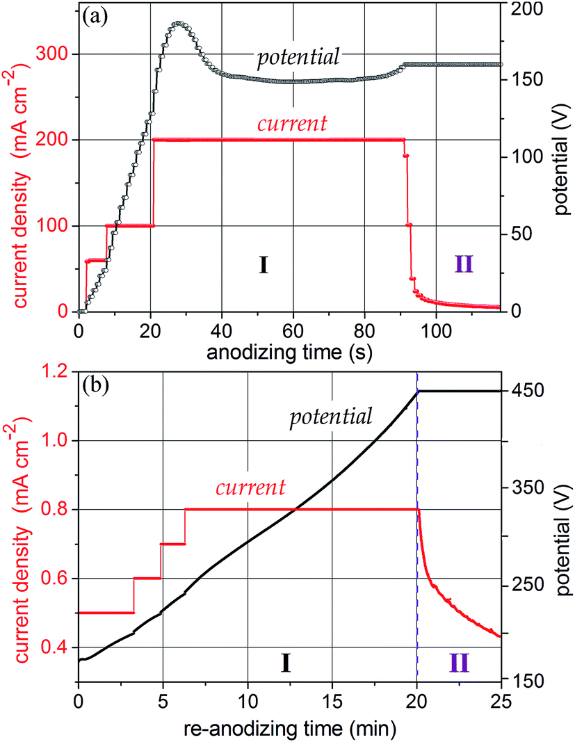 | ||
| Fig. 1 The potential–time and current–time responses for (a) anodizing and (b) re-anodizing in 0.2 mol dm−3 H3PO4 at 22 °C of Al (600 nm)/W (200 nm)/Ti (20 nm) metal layers sputter-deposited onto an oxidized Si wafer. | ||
The re-anodizing behavior of the same specimen is shown in Fig. 1b. To provide a uniform potential growth at a moderate rate, the current was stepwise raised up in the segment of 200 to 250 V. The systematic rise in the formation potential up to 450 V during the constant-current re-anodizing assumes the field-assisted growth of defect-free anodic oxide on the tungsten underlayer.
3.2 Film morphology
The first row of SEM images in Fig. 2 shows an anodic film derived from an Al/W/Ti/SiO2/Si sample anodized as shown in Fig. 1a, before and after selectively dissolving the alumina layer. Notably, the order of the alumina nanopores has been substantially improved due to the self-localized anodizing employed in this study. As a typical example, Fig. 2b demonstrates an array of well-aligned nanopores extended from the top to bottom of the thin alumina film, without branching inside or bending at the alumina surface, all being perfectly perpendicular to the substrate. Further, an array of nanosized protrusions (bulges), presumably of tungsten oxide, well ordered and separated by the tungsten metal at their bottoms are revealed in the micrographs of Fig. 2b–d. Each bulge consists of two parts – the upper, longer part above the Al2O3/W interface, which penetrates the alumina barrier layer, and the lower part below the interface, which forms as a local concave depression in the tungsten layer. Above the surface of the tungsten film, the bulges are surrounded by a continuous network of unoxidized aluminum, which remains after the completion of the anodizing process, as sketched later in Fig. 3c. An instability of TO growth is revealed in that some of the oxide bulges have an additional, tip-like region of material raised from their tops, pointed out by arrows in Fig. 2b. Likely, the tips consist of tungsten oxide because they extend from the surface of TO bulges developed by the PAA-assisted anodizing of the tungsten layer.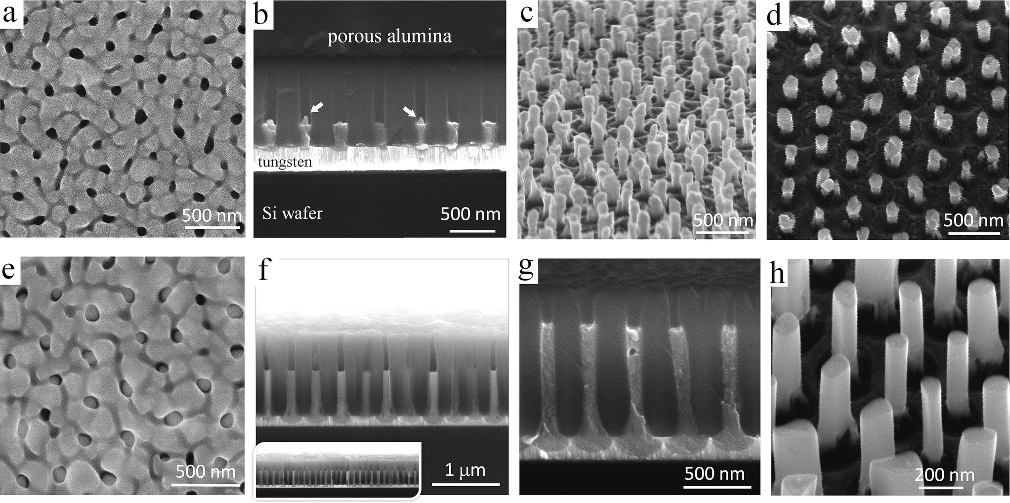 | ||
| Fig. 2 SEM images of anodic films derived from an Al/W/Ti trilayer (a–d) anodized as in Fig. 1a and (e–h) re-anodized as in Fig. 1b. The images in (c), (d), and (h) were recorded after the alumina layer had been selectively dissolved away. | ||
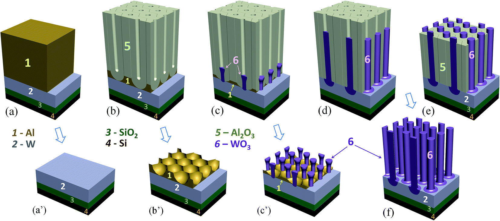 | ||
| Fig. 3 Schematic diagram showing the main steps for forming a metal-substrate-supported tungsten oxide (TO) nanorod array: (a) sputter-deposition of an Al/W/Ti trilayer (Ti not shown) onto a SiO2-coated Si wafer, (b) anodizing the Al layer to form a porous anodic alumina (PAA) film, (c) PAA-assisted anodizing of the W layer, (d) PAA-assisted high-voltage re-anodizing of the W layer to grow TO nanorods spatially separated by tungsten metal at their bottoms, (e and f) partial and complete dissolution of the PAA layer. Sketches in (a′), (b′), and (c′) give the samples' views after selective dissolution of the Al or PAA layers at stages (a), (b), and (c) respectively. | ||
However, the re-anodizing (as in Fig. 1b) results in lengthening the TO protrusions along the alumina pores in the form of vertically aligned, nearly cylindrical nanorods, all being essentially of the same height of 800 nm, an average diameter of 100 nm, and a population density of 7 × 108 cm−2, with flat tops and no hints of any instability at the electrolyte/oxide interface (Fig. 2e–h). Notably, the rods are directly anchored to the substrate metal, being well distanced and not merged in a continuous solid oxide layer, which is a unique situation at the PAA/metal interface achieved until now. A scheme developed with a computer-aided graphic program showing details of the process for forming substrate-metal-supported TO nanoarrays is outlined in Fig. 3.
In the course of SEM examination of numerous experimental samples and optimizing the formation conditions, it was revealed that the composition of rods is not uniform, such that the material inside the rods differs from that composing the outmost layer. To ‘look inside’ the rods, we etched to various extents the alumina of a selected sample, as depicted in Fig. 3e and f, to incompletely and then completely release the rods, cutting them off such as to directly observe their sections at different height levels. A typical situation that arises from the anodizing/re-anodizing of the Al/W layers is shown in the upper panel of images in Fig. 4. One may see that the rods are thin-walled nano-cylinders filled with a material, presumably tungsten oxide, from top to bottom.
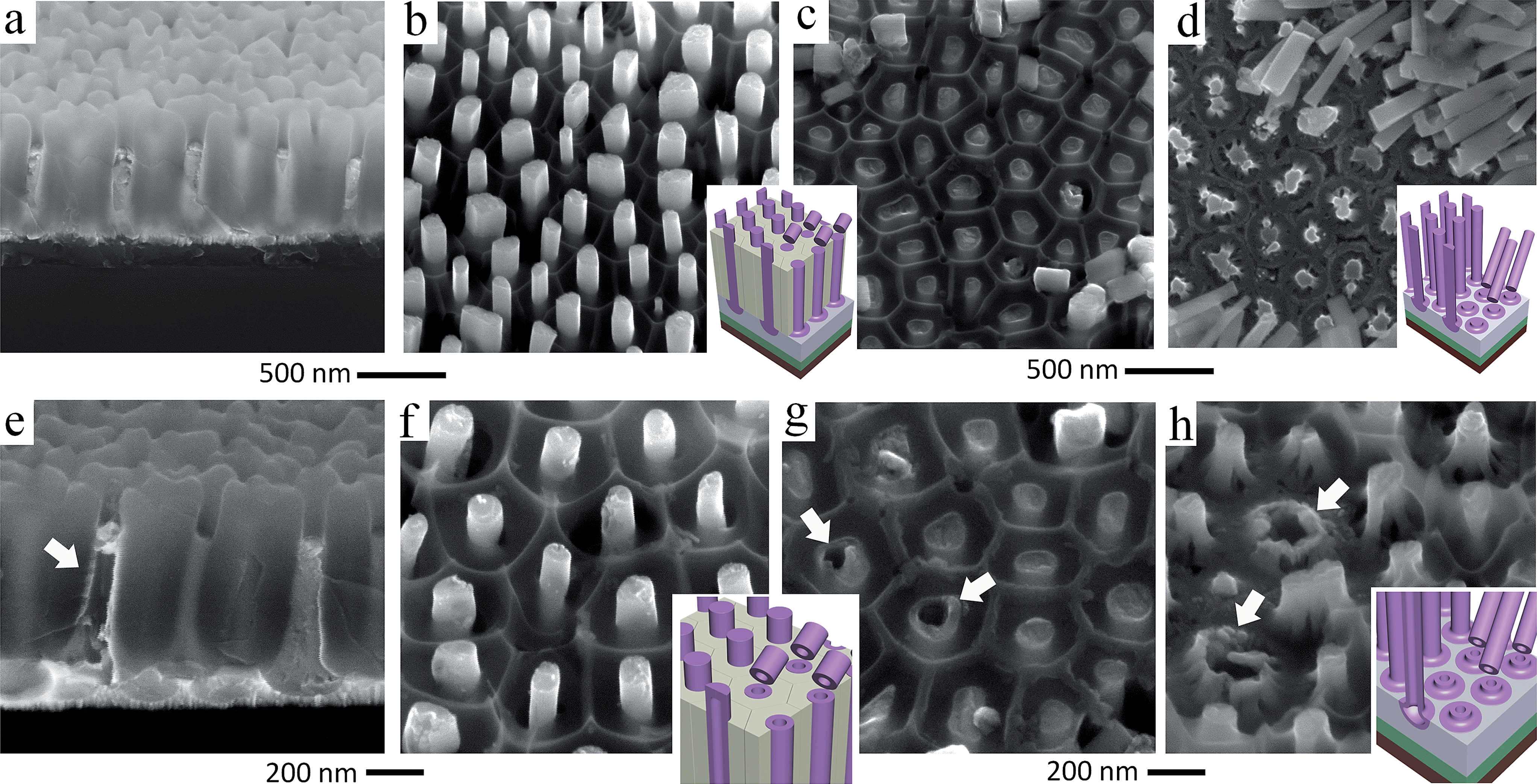 | ||
| Fig. 4 (a and e) Cross-sectional and (b–d, f–h) surface SEM images of the Al/W/Ti trilayers which had been re-anodized as in Fig. 1b and subjected to stepwise dissolution of the alumina layer followed by cutting off the TO nanorods to observe the inside of the rods. The lower panel of images shows the local formation of TO nanocapsules with closed tops and ‘empty’ interior. | ||
Locally, few ‘nanocapsules’ may develop in the alumina pores, that is, long-aspect-ratio top-closed nanotubes. At the first sight, the as grown nanocapsules look like the described-above nanorods (Fig. 4b and f). However, through the stepwise etching of the alumina film and breaking the rods, as shown in the lower row of SEM images in Fig. 4, it becomes clear that the inside of those rods is empty, i.e. not filled with a material (pointed out by arrows in Fig. 4e, g and h). The situation when the nanocapsules are likely to grow has been noticed at the edges of samples, where the local electrolytic conditions for processing the sample may deviate from those established for the bulk of the sample surface. Although the exact conditions for growing the capsules are not yet well understood, the local temperature, forming current density, and electrolyte concentration are among the factors that should be considered in detail in a future study.
The possibility to deliberately make the nanocapsules top-open arises through applying a post-reanodizing chemical treatment in a solution of pH about 7, which dissolves the caps and consumes the material inside the rods, thus ‘drilling’ nanochannels along the rods towards the metal substrate. The cylinder-like outer material of the rods remains intact as it is chemically more stable due to its mixed composition and more dense structure. The schematic diagram in Fig. 5 shows a range of the metal-oxide nanostructures that may derive from the same initial Al/W bilayer due to the differences in electrical and electrolytic formation conditions. The procedure for obtaining TO nanotubes and a mechanism of ionic transport and solid-state reactions at the electrolyte/film and film/substrate-metal interfaces will be discussed in Section 4.2.
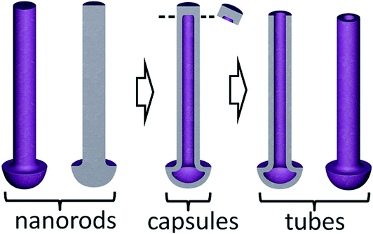 | ||
| Fig. 5 Schematic representation of a range of the metal-oxide nanostructures that may derive from the re-anodized Al/W bilayer due to the differences in electrical and electrolytic formation conditions. | ||
3.3 Chemical composition
Examination of the chemical composition and bonding states in the metal-oxide nanorods was performed by XPS. The specimens analyzed were (i) the air-annealed PAA-half-etched sample (as in Fig. 3e and 4b), (ii) the vacuum-annealed PAA-etched sample, (iii) the air-annealed PAA-etched sample, and (iv) the sample that was air-annealed after the PAA layer had been dissolved away. The presence of carbon, tungsten, oxygen, aluminum, phosphorous, and silicon was identified in the survey spectra of all the samples not sputter-cleaned prior to the analysis. Narrow-scan C 1s, W 4f, O 1s, Al 2p, P 1s, and Si 2p spectra were collected to analyze the core levels of the above elements. Gaussian (Y%)–Lorentzian (X%), defined in CasaXPS as GL(X), profiles were used for oxide components. For metallic core lines, asymmetry was defined in the form of LA (α, β, and m) where α and β outline the spread of the tail on either side of the Lorentzian component. The parameter m specifies the width of the Gaussian used to convolute the Lorentzian curve. A standard Shirley background was used in all fitted spectra. All binding energies were referenced to the C 1s at 285.0 eV generated by photoelectrons emitted from carbon atoms in C–H bonds. For all the unsputtered as-received surfaces, the peak-fitting of C 1s spectra was done as described in a previous study.21
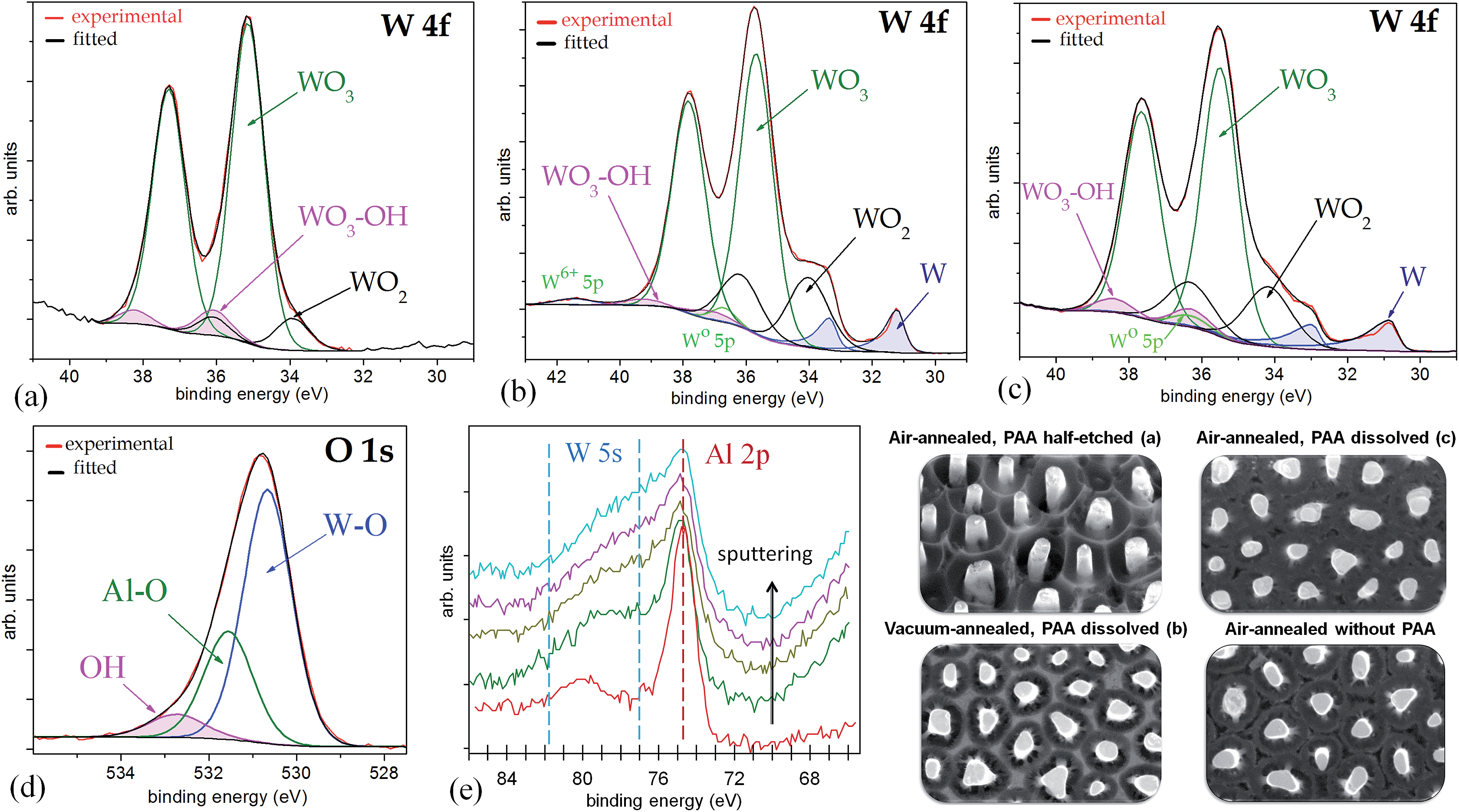
Fig. 6a shows a W 4f spectrum of the air-annealed PAA-half-etched sample surface (as in Fig. 3e and 4b), in which the photoelectrons are emitted only from the upper part of the rods. Three doublet peaks (W 4f7/2 and W 4f5/2) are used to reproduce the spectrum. Here and after, the W 4f5/2 peak for each species is constrained to be at a fixed energy increment of 2.15 eV above the W 4f7/2 peak, and the intensity ratio of the W 4f7/2 and W 4f5/2 peaks is fixed to 4![[thin space (1/6-em)]](https://www.rsc.org/images/entities/char_2009.gif) :3. The full widths at half maximum (FWHMs) for W6+ 4f7/2 and 4f5/2 peaks are set slightly narrower than those for the Wn+ 4f doublets where n < 6, since the structure of tungsten suboxides is thought to be loosely ordered.
:3. The full widths at half maximum (FWHMs) for W6+ 4f7/2 and 4f5/2 peaks are set slightly narrower than those for the Wn+ 4f doublets where n < 6, since the structure of tungsten suboxides is thought to be loosely ordered.
 | ||
| Fig. 6 Experimental and curve-fitted XP spectra of (a) W 4f for the unsputtered air-annealed PAA-half-etched sample (as in Fig. 3e), (b) W 4f for the unsputtered vacuum-annealed PAA-full-etched sample (as in Fig. 3f), (c) W 4f for the unsputtered air-annealed PAA-full etched sample (as in Fig. 3f), (d) O 1s for the sputter-cleaned air-annealed PAA-full-etched sample, (e) Al 2p for the sputter-profiled air-annealed PAA-full-etched sample. The SEM images show the evolution of surface morphology of the differently treated samples. | ||
The highest-intensity doublet with binding energies of 35.15 eV (W 4f7/2) and 37.30 eV (W 4f5/2) is associated with photoelectrons emitted from W6+ ions, i.e., stoichiometric WO3.31 The lowest-energy doublet at 33.93 (W 4f7/2) and 36.08 eV (W 4f5/2), shifted to −1.22 eV from the dominating spectrum component, is associated with photoelectrons emitted from W atoms with +4 oxidation state (W4+) in WO2.32 The highest-energy doublet with components at 36.1 eV (W 4f7/2) and 38.25 eV (W 4f5/2) can be associated with the presence of hydroxyl groups bonded with tungsten W–(OH)2, which remain after the decomposition of oxide–hydroxide compounds WO3·(OH2)n−, or ‘tungstic acids’.1,6 No peaks attributed to metallic W are identified in the spectrum.
Fig. 6b shows a W 4f spectrum of the vacuum-annealed PAA-etched sample surface (as in Fig. 2h). The highest-intensity doublet with binding energies of 35.67 eV (W 4f7/2) and 37.82 eV (W 4f5/2) dominates in the spectrum and is assigned to the W3+ oxidation state (WO3). At the lower energy edge, the doublet at 31.20 and 33.35 eV is associated with W0 4f7/2 and 4f5/2 electrons emitted from W0. Besides, the spectrum reveals two more chemical shifts from the bulk level, which correspond to tungsten suboxides. A doublet with a peak binding energy of 34.02 eV (W 4f7/2), shifted to +2.82 eV from the metal level is assigned to the W4+ oxidation state (WO2). The highest-energy doublet at 37.1 eV (W 4f7/2) may again be associated with the hydroxylated part of the tungsten oxide. Since the W 4f spectrum contains the metal and oxide species, additional components corresponding to the W0 5p3/2 and W6+ 5p3/2 peaks are factored (with their RSF set to 0) at 5.5 eV above the W0 4f7/2 and W6+ 4f7/2 peaks, respectively.
The W 4f spectrum of the air-annealed PAA-etched sample shown in Fig. 6c is similarly reproduced by the four doublets associated with photoelectrons emitted from W6+, W4+, W0 (WO3, WO2, W), and W–OH bonds. The difference, however, between the air- and vacuum-annealed samples is in the percentage of spectral components: the concentration of WO3 hydrates decreases from 7.4 to 2.2 at% while the concentration of WO2 increases from 17.5 to 20.5 at% due to the annealing in a vacuum.
Complementing the set of XPS analysis data, the W 4f core-level spectrum was recorded for the sample that was PAA-etched prior to air annealing at 550 °C (not shown). Following the above interpretation, the spectrum is reproduced by the two doublet peaks associated with WO3 (dominating amount) and W–OH (minor amount). Neither tungsten suboxides nor metal is detected. This implies that when the rods are exposed to air atmosphere under the given thermal conditions and without the alumina overlayer, the oxygen molecules absorb on the surface of the rods, diffuse inside, restore the oxide stoichiometry, and oxidize to some extent the surface of tungsten metal surrounding the columns.
The O 1s spectra of unsputtered surfaces of the air- and vacuum-annealed PAA-etched samples were very complex. In the air-annealed sample, besides the usual O 1s peak components due to H2O (chemisorbed water) at 533.5 eV and OH (hydroxylated region) at 532.4 eV, there were two more well-resolved peaks of relatively higher intensities in the lower-energy range. The most intensive peak at 530.7 eV is assigned to oxygen species O2− in WO3 while the smaller peak at 531.6 eV is assigned to O2− species bonded with Al3+(Al2O3). With the Ar ion sputtering of the air-annealed (PAA-free) sample (Fig. 6d), the relative intensity of the Al2O3-associated peak decreased, likely due to the gradual removal of the alumina-containing outmost layer. Further, the higher-energy H2O-associated peak is not present, and a singlet peak at 532.8 eV is assigned to the hydroxylated part of the tungsten oxide. The presence of hydroxyl oxygen revealed clearly in the O 1s spectra is obviously due to OH bonded with WO3, as also confirmed by the analysis of the W 4f core-level spectrum.
The Al 2p spectra of both the air- and vacuum-annealed PAA-etched samples are well reproduced by a singlet with a binding energy of 74.6 eV, which is associated with Al2O3. When the air-annealed specimen is Ar+ ion sputtered (Fig. 6e), the Al3+ peak intensity monotonically decreases, the peak being still identified until the 10th sputter cycle. An interesting feature is that, close to the Al 2p peak, there is a broad additional peak in the energy window of 77–82 eV, which is associated with 5s electrons emitted from tungsten oxides. This peak becomes even broader and more intensive when the sample surface is Ar-ion sputtered (Fig. 6e). From the Al 2p/W 5s profiling behavior it is obvious that alumina is incorporated in the outer layer of the material, being mixed with tungsten oxides and dispersed along the rod length. The Al 2p/W 5s core-level spectra also suggest that aluminum tungstate 2Al2O3·5WO3 is formed, the phenomenon being discussed in detail in Section 4.2.
An amount of adventitious carbon and the minor atomic concentrations of P and Si were detected on the unsputtered surfaces of the annealed PAA-free samples. The adventitious carbon contamination was used as a charge reference for all the XP spectra. However, neither of the above elements was detected by recording the corresponding high resolution spectra of all the samples already after the first sputter-cleaning cycle. This confirms that carbon, phosphorus, and silicon were present only in the outermost layer of the organic contamination, incomparable even with the depth of alumina incorporation.
Conclusively, the XPS analysis of the 550 °C-air-annealed samples reveals that the TO nanorods are mostly composed of stoichiometric WO3 and surrounded at their bottoms by the substrate tungsten metal. The rods also comprise relatively smaller amounts of WO2 located in the outer layer and on the top of the rods. The tungsten oxides are mixed with the minor amount of Al2O3 in the outmost region while the inner material of the nanorods is mostly hydroxylated tungsten oxide derived from the thermally modified WO3·nH2O oxide–hydroxide component. Likely, aluminum tungstate, Al2(WO4)3, is formed in the nanorods. The annealing in a vacuum results in increasing the portion of WO2 and decreasing the portion of hydroxylated oxide, the WO3 component being still dominating, at least at the surface region. The nanorods are free from any electrolyte- and substrate-derived impurities, such as metallic W, Ti, Al, Si, or P. A mechanism that explains the formation and chemical composition of the oxide nanorods is presented in Sections 4.1 and 4.2.
3.4 Crystal structure
Fig. 7 shows the experimental, calculated, and difference diffractograms of the as-anodized, air-annealed, and vacuum-annealed samples, together with the 2-D diffractograms, from which the conventional diffractograms were obtained. The crystal structure for each phase found in the ICSD database (FIZ, 2015), the main refined parameters, and details of the XRD profile line and quantitative phase analysis are listed in the ESI.†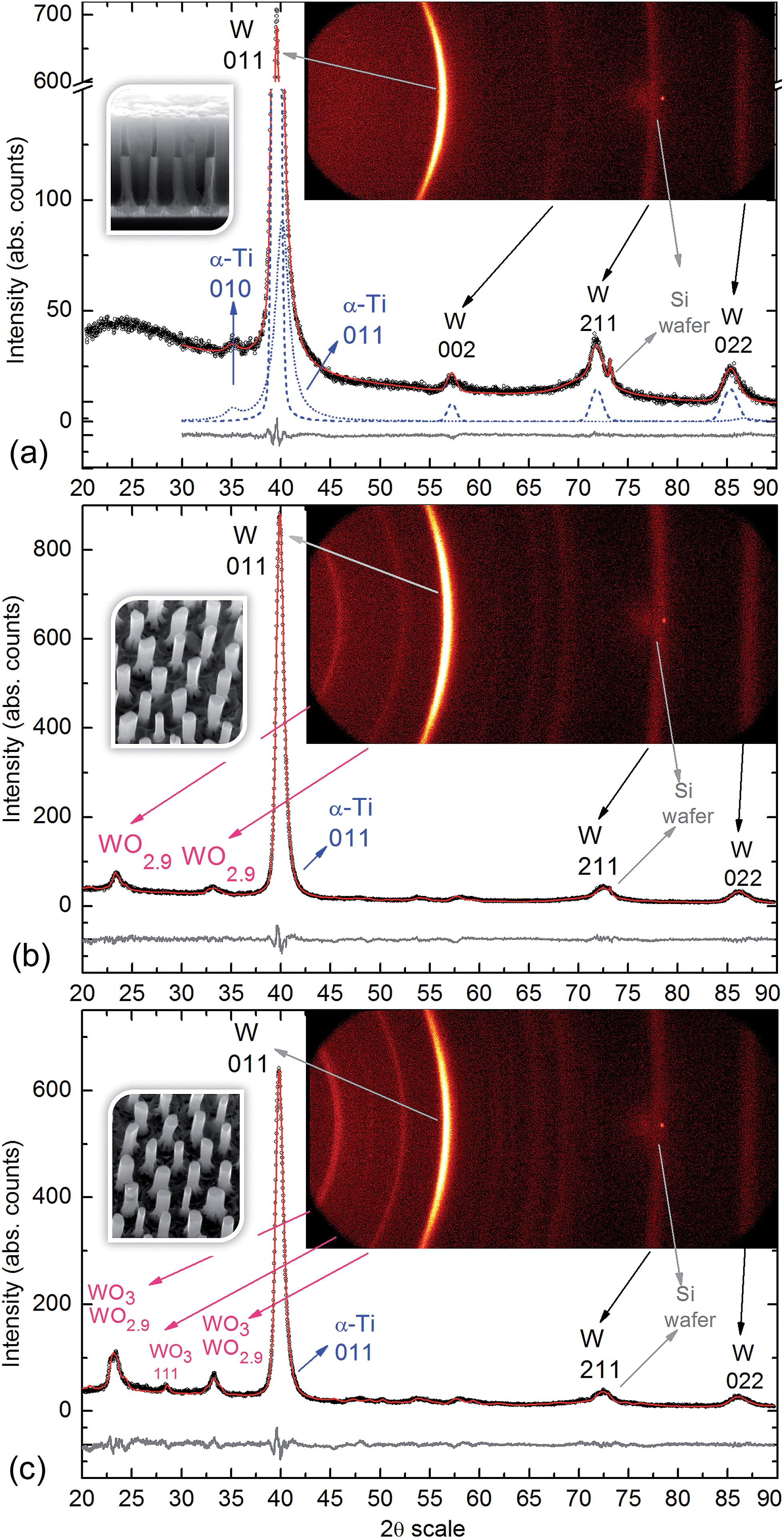 | ||
| Fig. 7 X-ray diffractograms of the (a) as-anodized, (b) vacuum-annealed, and (c) air-annealed samples. Insets: 2-D diffractograms and SEM images of the corresponding films. Symbols: circles – conventional diffractograms resulted from the γ integration of the 2-D diffractograms; red solid line – calculated diffractograms; grey lines underneath – difference diffractograms; blue dashed line – calculated diffractogram for W phase; blue dotted line – calculated diffractogram for α-Ti phase. The arrows relate the observed Debye rings of the 2-D diffractogram with the corresponding peaks of the conventional diffractograms. The hkl indices of main reflections are also indicated. | ||
Fig. 7a shows the resulting diffractogram in the range of 20–90° 2θ angles of the as-anodized (not annealed) sample, as sketched in Fig. 3d. The main peak at 39.6° 2θ exhibits an asymmetry at high angles that can be explained neither by the instrumental effects nor by the presence of W only (cubic, space group (sg) Im![[3 with combining macron]](https://www.rsc.org/images/entities/char_0033_0304.gif) m). We assume that the asymmetry is due to the presence of α-Ti (hexagonal, sg P63/mmc) in such a way that the reflection (011) of α-Ti is almost overlapped by the reflection (011) of W. It is known that α-Ti is a low temperature phase that transforms to β-Ti (cubic, sg Imm) at about 1155 K. By introducing this second phase (α-Ti), the asymmetry is easily modelled. The presence of α-Ti is also confirmed by a small broad peak at 35° 2θ produced by the (010) reflection of α-Ti. Both phases were corrected for preferred orientation, as would be expected by the synthesis process. The amount of α-Ti was estimated by the Rietveld method to be about 4.5%, high enough to produce an asymmetry effect of the main diffraction peak of W. The microstructure of both phases was estimated from peak broadening. We observed for the W phase an important contribution of the microstrain, e0, to the peak broadening that was estimated to be 3.43(5) × 10−3, whereas the contribution of the crystallite size to the peak broadening was of 68.3(8) nm. For α-Ti we considered only the crystallite size to the peak broadening resulting in 4.3(1) nm. We cannot estimate the microstrain contribution to the peak broadening of α-Ti because of the lack of well resolved peaks for this phase. We can consider that the crystallites of α-Ti are smaller than the crystallites of W. The microstrain detected for tungsten can be interpreted as a result of the synthesis process. Apparently, the two phases detected for this sample are associated with a portion of the substrate metals that have been produced by r.f. magnetron sputter-deposition and remain partly unoxidized after the anodic treatment. In the analyzed range, there is no evidence of peaks associated with any crystalline phases of Al2O3, TiO2, or WO3 (at the available detection limit). This implies that the oxides composing the anodic film are amorphous. These findings underline the importance of having high quality and purity precursor materials (Ti, W), with known crystalline structures and physically and electronically sharp interfaces, prepared via magnetron sputter-deposition technique for the successful and reproducible anodic synthesis of metal-oxide nanofilms.
m). We assume that the asymmetry is due to the presence of α-Ti (hexagonal, sg P63/mmc) in such a way that the reflection (011) of α-Ti is almost overlapped by the reflection (011) of W. It is known that α-Ti is a low temperature phase that transforms to β-Ti (cubic, sg Imm) at about 1155 K. By introducing this second phase (α-Ti), the asymmetry is easily modelled. The presence of α-Ti is also confirmed by a small broad peak at 35° 2θ produced by the (010) reflection of α-Ti. Both phases were corrected for preferred orientation, as would be expected by the synthesis process. The amount of α-Ti was estimated by the Rietveld method to be about 4.5%, high enough to produce an asymmetry effect of the main diffraction peak of W. The microstructure of both phases was estimated from peak broadening. We observed for the W phase an important contribution of the microstrain, e0, to the peak broadening that was estimated to be 3.43(5) × 10−3, whereas the contribution of the crystallite size to the peak broadening was of 68.3(8) nm. For α-Ti we considered only the crystallite size to the peak broadening resulting in 4.3(1) nm. We cannot estimate the microstrain contribution to the peak broadening of α-Ti because of the lack of well resolved peaks for this phase. We can consider that the crystallites of α-Ti are smaller than the crystallites of W. The microstrain detected for tungsten can be interpreted as a result of the synthesis process. Apparently, the two phases detected for this sample are associated with a portion of the substrate metals that have been produced by r.f. magnetron sputter-deposition and remain partly unoxidized after the anodic treatment. In the analyzed range, there is no evidence of peaks associated with any crystalline phases of Al2O3, TiO2, or WO3 (at the available detection limit). This implies that the oxides composing the anodic film are amorphous. These findings underline the importance of having high quality and purity precursor materials (Ti, W), with known crystalline structures and physically and electronically sharp interfaces, prepared via magnetron sputter-deposition technique for the successful and reproducible anodic synthesis of metal-oxide nanofilms.
For the air-annealed PAA-etched sample (sketched in Fig. 3f), the detected peaks are from the WO3 phase (monoclinic, sg P21/n, crystallite size 18.6 nm) and the WO2.9 phase (monoclinic sg P2/c, crystallite size 5.2 nm), additionally to the metallic α-Ti and W peaks originating from the substrate metals that remain unoxidized after the air-annealing treatment (Fig. 7c).
For the vacuum-annealed PAA-etched sample (Fig. 7b), the diffraction peaks are from the same WO2.9 phase, although the crystallite size is relatively bigger (6.8 nm) and, again, from the metallic α-Ti and W phases associated with the substrate metals.
Comparing the wt% ratio between the W and α-Ti phases in the as-anodized (21.2) and air-annealed (12.5) samples, one may conclude that the amount of metallic tungsten that remains after the anodizing is relatively smaller in the air-annealed sample, which is likely due to partial thermal oxidation of the tungsten layer. The crystallite size in the α-Ti increases from 4.3 nm to 7.7 and 6.8 nm due to the annealing, which corresponds to a typical impact of the recrystallization process. The microstrain (e0) for the W phase also shows a normal temperature-dependent behavior, decreasing from 3.43 × 10⁻³ to 2.96 × 10⁻⁵ and 2.57 × 10⁻⁵. Contrarily to the α-Ti phase, the crystallite size in the W phase appears to decrease in the annealed samples (45.2 and 57.3 nm) relative to the as-anodized sample (68.3 nm).
The XRD analysis reveals clearly that the amorphous TO in the as-anodized nanorods crystallizes due to the annealing at 550 °C. The formation of WO2.9 phase in the vacuum-annealed sample results partially from oxygen release into the gas phase at low pressures and from temperature-assisted diffusion of oxygen ions from WO3 towards the substrate and their dissolution in the tungsten layer. The same phenomena occur during the heating in air, although to a smaller extent, competing with the thermal oxidation of tungsten at the oxide/metal interface and, at a higher partial pressure of O2, filling the oxygen vacancies in the WO3. Thus, after cooling down the samples, the two monoclinic crystalline phases, WO2.9 (∼37 wt%) and WO3 (∼14 wt%) co-exist in the oxide nanorods. From comparison of the XPS and XRD results, it is likely that a portion of WO3 still remains amorphous, being mixed with amorphous Al2O3 and located at the surface layer. Another important finding is that a portion of the W/Ti bilayer remains unoxidized beneath and around the bottoms of the rods, in the amount of ∼57 and ∼45 wt% in the vacuum-annealed and air-annealed samples, respectively.
3.5 Electrochemical properties
For determining semiconducting properties of the TO nanoarrays, EIS and Mott–Schottky analyses were performed on the air- and vacuum-annealed PAA-containing samples, as depicted in Fig. 3d and 4a. Due to the uncertainty in the applied potential value associated with the two-electrode configuration employed and the complexity of equivalent circuits, Mott–Schottky analysis was mainly applied to estimate the semiconducting properties and to determine the dopant level in the TO nanoarrays.Fig. 8b and c shows the Bode diagrams recorded for the air- and vacuum-annealed samples. The EIS data for the air-annealed sample are best fitted with a circuit containing three R–CPE loops connected in series, showing the presence of three capacitive layers in the sample (Fig. 8b): one with a high parallel resistance (107 to 109 Ω cm2) and two others with low parallel resistances (103 to 105 Ω cm2). A constant phase element (CPE) was used in the circuit in order to account for frequency dispersion, and the effective capacitance was calculated and used for evaluation. From the analysis of the C(V), 1/C2(V), and R(V) dependences (linear 1/C2(V), high R increasing with the potential), we conclude that the capacitive layer with the highest resistance is consistent with a charge depletion layer that is thinner than the total film thickness and forms at the tops of the rods, as shown in Fig. 8a. The other capacitive layers are associated with the double layers at the sample surface and at the gold counter electrode (see ESI† for further evaluation and more discussion).33
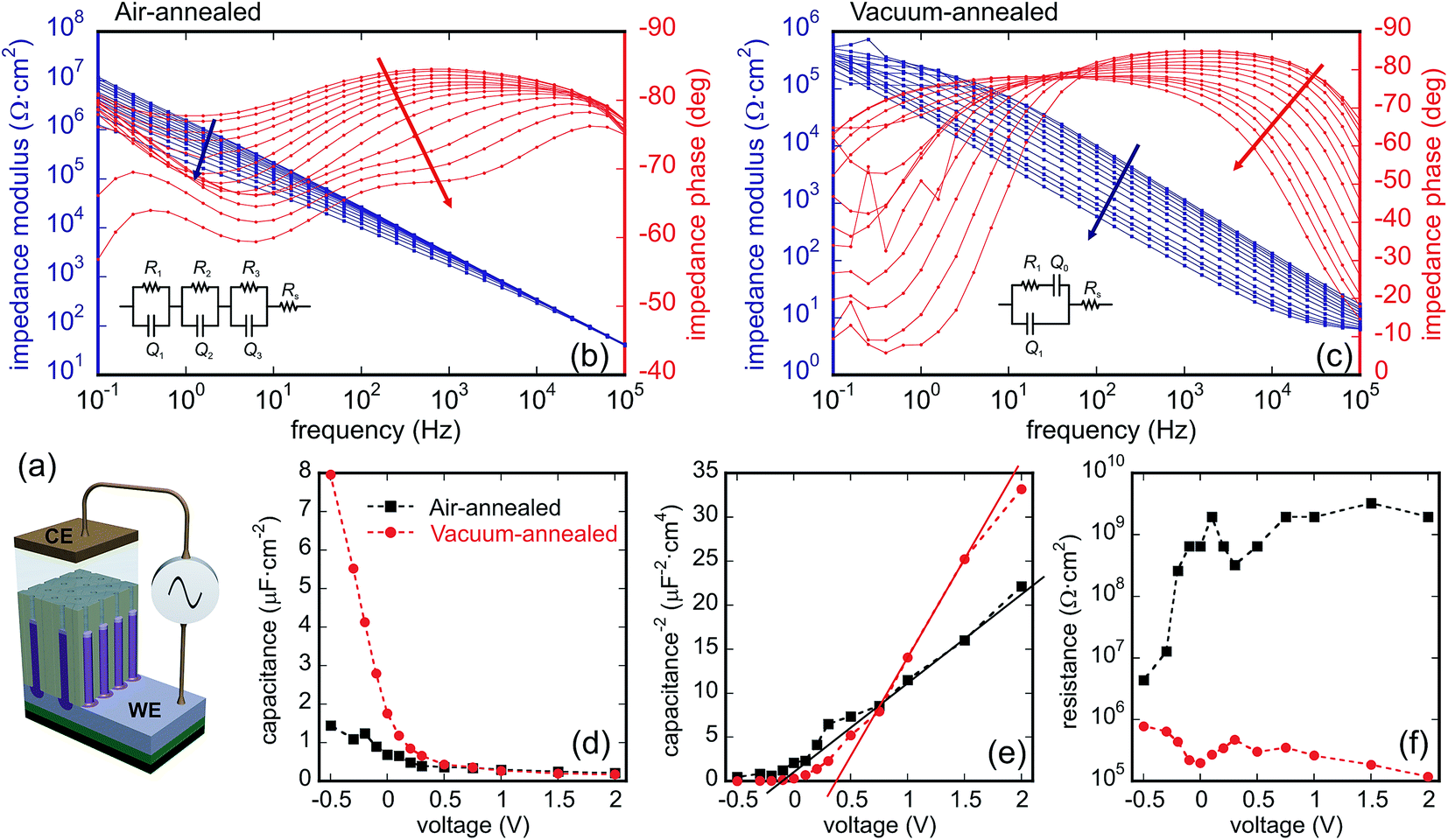 | ||
| Fig. 8 (a) Schematic representation of the microcell used for EIS measurements. (b and c) Bode diagrams recorded at bias potentials from 2.0 to −0.5 V (arrow direction) in 0.1 M Na2SO4, pH 5, of the air- and vacuum-annealed PAA-incorporated TO nanorod arrays. The insets show equivalent circuits used for data fitting and evaluation. (d–f) Three plots showing the behavior of the calculated potential-dependent parameters (d) C(V), (e) 1/C2(V), and (f) R(V). | ||
The EIS data of the vacuum-annealed sample were fitted most satisfactorily with a circuit of one R–CPE loop, having an additional CPE in series with the resistance (Fig. 8c). One of the two time constants (the one being in parallel with the resistance) is certainly associated with a charge depletion layer at the top of the rods, due to their C(V), 1/C2(V), and R(V) behavior (see ESI† for more discussion). The C(V), 1/C2(V), and R(V) dependences associated with the space-charge layer behavior of the two samples are shown in Fig. 8d–f. Both samples are characterized by a positive slope in the Mott–Schottky plot (1/C2(V)), as expected for an n-type semiconductor. The air-annealed sample shows relatively smaller slope, suggesting an increased donor density, Nd, based on the Mott–Schottky equation,
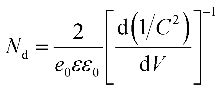 | (1) |
4 Discussion
4.1 Semiconductor properties
According to the point-defect model,34 the electronic conduction in an n-type metal-oxide semiconductor originates from the presence of oxygen vacancies and/or interstitial metal ions acting as electronic dopants. On the first sight, the higher donor density revealed in the air-annealed nanorods relative to the vacuum-annealed nanorods by Mott–Schottky analysis contradicts the above model since higher donor densities are usually associated with vacuum-annealed WO3 nanostructures. The ‘inverse’ Nd behavior may be explained through the following consideration. The oxygen vacancies in WO3 acting as electron donors and leading to a substoichiometric composition of the oxide are present as point defects at lower amounts. However, higher concentrations of oxygen vacancies in the annealed oxides lead to their accumulation in shear planes (Wadsley defects), randomly present in the structure, whereas some of the corner-sharing WO6 octahedra transform into edge-sharing ones. When reaching the composition of WO2.9, the shear planes become distributed periodically, altering the crystal structure. It is claimed in the literature that the shear planes lead as well to an increase in the charge carrier concentration and thus increase the conductivity.35,36 Experimentally determined conductivities of 10 to 10−4 and 103 S cm−1 were reported for differently doped WO3 (ref. 1) and WO2.9 (ref. 37) oxides, respectively. In our work, a several orders of magnitude difference in the depletion layer conductivity is revealed as well by the EIS measurements of the air- and vacuum-annealed TO nanoarrays comprising the WO3 and WO2.9 phases, respectively, at the tops of the nanorods. Moreover, a similarly high difference was revealed in conductivities of these TO nanostructures assembled in solid-state microdevices based on metal-semiconductor/metal (MSM) microcells; this will be reported in our future study.In contrast, the donor densities obtained by the EIS measurements appear to be of the same order of magnitude in the two types of the nanoarrays. Since no Mott–Schottky estimation of Nd for the WO2.9 phase is found in the literature, we assume that the formation of shear planes in the WO2.9 crystal structure may lead actually to elimination of the oxygen vacancies,38 thus causing a lower donor density, as expected from the oxide stoichiometry.
4.2 Mechanism of film growth
A model of nucleation and growth of the metal-substrate-separated TO nanorods, nanocapsules, and tubes is proposed and discussed in this section, based on the findings of previous studies,39–41 with help of a diagram in Fig. 9. According to the model, over the first current decay during the anodizing (Fig. 1a), TO grows due to the local oxidation of tungsten layer under the pores. At these sites, the tungsten oxidizes with a large volume change and a column of tungsten oxide is forced into the alumina barrier layer (Fig. 9a). The width of the column depends upon the pore size and dimension of the site of exposed tungsten, which will enlarge as oxidation proceeds. The column continues to grow provided it can retain a significant current compared with the adjacent alumina. This is possible as long as there is aluminum remaining. As the amount of aluminum is reduced, the regions of tungsten metal exposed to oxidation increase, this being followed by the thickening of the oxide by displacement of and mixing with alumina above a growing column. The local consumption of tungsten proceeds at a faster rate than the oxidation of the adjacent aluminum since anodic TO has lower ionic resistivity than anodic alumina.41,42 The SEM (Fig. 2) and XPS results (not shown here) confirm that a net-like aluminum layer remains around the TO protrusions after completing the first anodizing step (sketched in Fig. 3c), confining the growth of bottom parts of the TO nanorods and not allowing them to merge (Fig. 9a).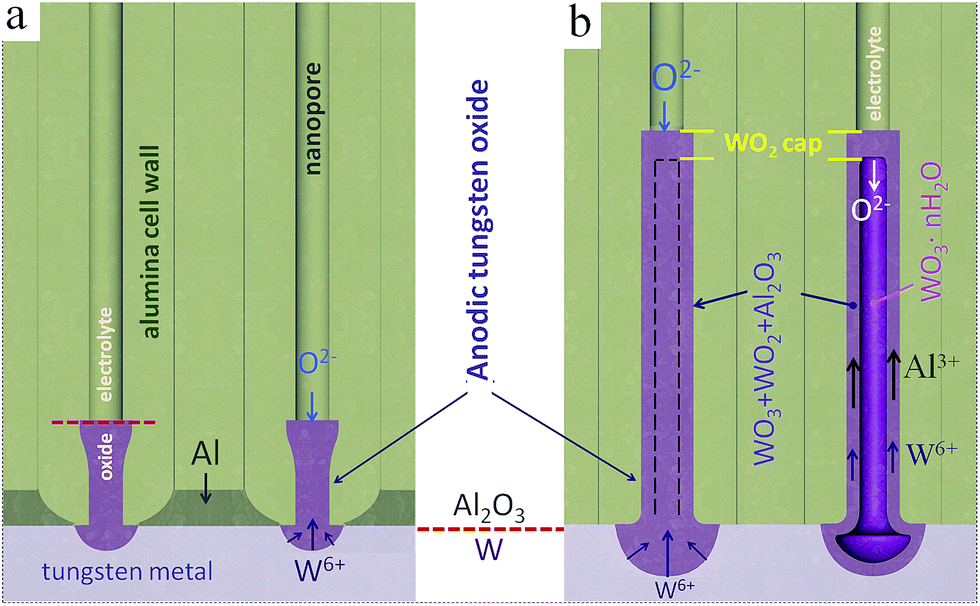 | ||
| Fig. 9 Schematic model of oxide growth and ionic transport processes during the anodization/re-anodization of an Al/W bilayer as in Fig. 1: (a) the formation of TO protrusions at the Al2O3/W interface, (b) the formation of PAA-assisted TO nanorods (nanocapsules) via re-anodization of the W underlayer. | ||
During the re-anodizing (Fig. 1b), the W layer is further consumed and new, rod-like oxide continuously forms and is directed into the pores via cross-migration of W6+, Al3+, and O2− ions, with the expanding of the pre-existing migration pathways in the alumina barrier layer. The adjacent aluminum is oxidized slowly during the re-anodizing, and is completely consumed only when the potential reaches about 350 V. The slow oxidation rate of the adjacent aluminum is an explanation why the TO nanorods grow well separated by the remaining tungsten metal till the end of the re-anodization process. Due to the differences in ionic conduction between the outer and inner parts of the alumina cells,18 the tungsten and aluminum cations migrate within a ‘contaminated’ part of the alumina cell wall, which decides the outer shape (diameter) of the rods and results in the mixed composition of the outer layer (WO3 + Al2O3). Furthermore, aluminum tungstate Al2(WO4)3 may form due to reaction of WO3 with Al2O3, as derived from the XPS analysis.
The development of anodic tungsten oxide above and beneath the film/metal interface is determined by a combination of the WO3/W volume expansion factor, the transport numbers for tungsten species, and the ratio of ionic resistances of the TO and alumina encircling the columns.41 Considering a large Pilling–Bedworth ratio (PBR) of 3.6 for W/WO3 and even suggesting an increased transport number for W6+ cations of ∼0.48,18 it is not obvious why such a large volume of the oxide forms above the Al2O3/W interface, i.e. inside the pores. In our opinion, the explanation lies in the difference in composition of the outer and inner material of the rods. While the outer layer of the rods is mainly composed of WO3, WO2, and Al2O3, the inner material consists of tungstic acid WO3·nH2O, which has a flimsy structure and obviously larger PBR relative to WO3. Moreover, it is known that, in neutral and especially acidic aqueous solutions, aluminum tungstate Al2(WO4)3 may give the heteropoly acids and polyoxometalate anions.43 An unstable, very soluble metatungstate anion, [H2W12O40]6−, is formed; the inclusion of a different atom such as aluminum or phosphorus in place of the two central hydrogens in metatungstate may produce large molecules, for example phosphotungstic acid H3PW12O40,44 which might also contribute to expanding the material inside the rods.
The ‘caps’ that close the rods or capsules (Fig. 9) prevent the inner material from being dissolved already during the re-anodizing process. Likely, the caps are first developed at the commencement of re-anodizing and then remain on the surface of the oxide nanorods. It is not immediately obvious how the caps move outward when the rods grow up. A possible interpretation of this paradoxical feature is to consider the difference in the electrochemical properties of the caps and the inner material composing the rods. From the XPS results, the caps contain or may be mostly composed of tungsten suboxide WO2, which prevents outward migration of W6+ ions and makes the growth of anodic TO at the electrolyte/film interface impossible or negligible. If this is the case, the growth of the rods occurs merely due to inward migration of O2−, and OH− ions and electrolyte-derived species. Thus, the oxide grows mainly under the caps, pushing the caps outward, similarly to the situation described by Habazaki et al.45 for compact anodizing of Al–Hf alloys.
4.3 Oxide growth beyond the pores
The inner material may grow in the rods independently in some sense from the outer material, which is developed via migration of W6+ and Al3+ ions in the anodic alumina. When the rods reach the surface of the alumina film, the caps lose their contact with the cell walls, and the kinetics of TO growth changes dramatically. The inner material of the rods becomes no longer pore-directed, ‘breaks’ the cap, and continues to grow as a protuberance coming out from the pore in the form of exotic nanothread or curved nanowire, as seen in SEM images in Fig. 10. This unique phenomenon gives us a better understanding of what material forms inside the rods. Analysis of the W 4f XP spectrum recorded at the surface of such a film (Fig. 10e), confirms the presence in the protuberances of a substantially larger amount of WO3·2H2O (31 at%), and WO2 (27 at%) relative to the 7 and 17 at% respectively in the ‘normally’ prepared, air-annealed TO nanorods (Fig. 6c). Analysis of the W 5s core-level spectrum of this sample (Fig. 10g) gives a number of components in the intensive well-defined W 5s peak arising from tungsten atoms existing in several oxidation states, and further supports the previously made suggestion that aluminum tungstate forms inside the rods.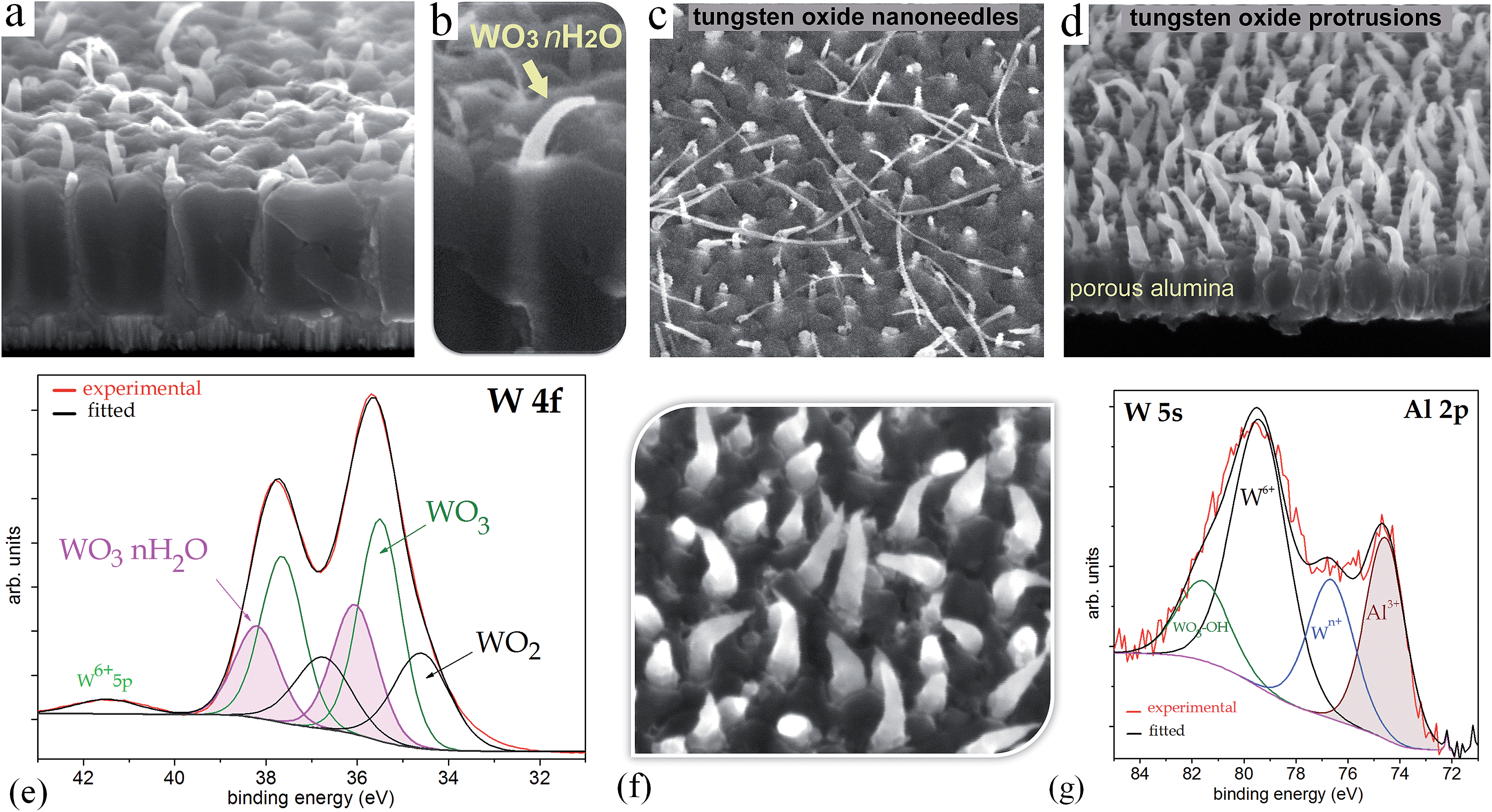 | ||
| Fig. 10 (a–d) and (f) SEM images showing the growth of TO protuberances over the general surface of the alumina film and the results of their XPS surface analysis: (e) W 4f and (g) Al 2p/W 5s core-level XP surface spectra of a TO protuberance sample as imaged in (d) and (f). | ||
It is known that tungstic acids (WO3·nH2O) decompose already at about 200 °C giving amorphous WO3 or resulting in monoclinic WO3 at 400 °C.15 However, the XPS analysis performed in the present work undoubtedly shows the presence of OH-groups in the composition of the TO nanorods annealed at 550 °C. According to Shpak et al.,6 OH and H2O may remain only in the annealed nonstoichiometric WO3−x oxides because the oxygen vacancies may be filled by OH-groups, and their amount is proportional to the degree of nonstoichiometry (x-value). Structurally, the W5+ cation should be in the center of an octahedron built up of five O2− and one OH− ion.6 The result can be expressed as Wx5+W1−x6+O3−x(OH)x, where x is the number of hydroxyl groups that fill the oxygen vacancies.6
A modified point-defect model46 involves the formation and/or annihilation of hydroxyl vacancies, at the film/metal and solution/film interfaces, respectively. The experimentally determined values of the oxygen vacancies and hydroxyl vacancies diffusivities in the passive films appeared to be of the same order of magnitude.46 Thus, one may expect that the hydroxylation of the TO nanorods impacts substantially their chemical, structural, and electronic properties. For instance, it has been reported that OH− anions that are present in TOs in enlarged amounts greatly influence catalytic and electrochemical activity of the oxides.47 The compositional-structure-functionality of the TO nanoarrays assembled in MSM microcells will be described in a future study.
4.4 From nanocapsules to nanotubes
Returning to the formation of TO nanotubes, we would like to stress that the tops of the TO capsules may be deliberately perforated such as to transform the capsules to open-top nanotubes. This may be achieved either via the field-assisted oxide dissolution inside the pores or by chemical etching in a solution. Fig. 11a–c shows how the tops of the capsules change in the course of electrochemically perforating the caps, performed prior to dissolution of the alumina layer. For doing so, after the re-anodizing, an anodic polarization is applied to the tungsten metal in a phosphate buffer solution of pH near 7 at a potential equal to or higher than the formation potential, for a period of about 20 min, ending when the anodic current begins to rise at a progressively increasing rate, up to about 0.5 mA cm−2. The cross sectional SEM image of Fig. 11d demonstrates the result of transforming the capsules to tubes before the alumina host is dissolved.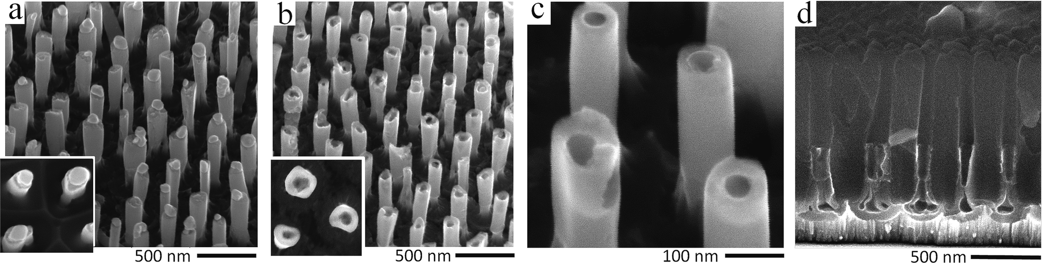 | ||
| Fig. 11 SEM images of an anodic film derived from an Al/W/Ti trilayer that was anodized and re-anodized through the alumina nanopores to 450 V to grow TO nanocapsules which were then electrochemically top-opened and transformed to nanotubes. The treatment to open the tops of the capsules was carried out via anodic polarization of the tungsten layer in a phosphate buffer solution of pH 7 for a period of 20 min: (a) nanocapsules with partly etched tops, (b and c) nanocapsules with fully opened tops, (d) open-top nanotubes incorporated yet in the alumina overlayer. | ||
5 Conclusions
(1) In this work we have demonstrated that an Al/W bilayer can be anodically processed in such a way that it allows the growth of a self-organized array of long-aspect-ratio TO solid-state nanorods or nanocapsules with closed tops and ‘empty’ interior, which can be electrochemically top-opened and thus transformed to TO nanotubes, vertically aligned and spatially ordered on a conducting substrate. The as-anodized nanorods are composed of amorphous WO3 mixed with minor amount of Al2O3, WO2, and tungsten-oxide hydroxide compound WO3·nH2O, being free from electrolyte-derived impurities. Annealing the films in air and vacuum at 550 °C increases the portion of suboxides and oxide hydrates and gives the formation of monoclinic WO3 + WO2.9 and WO2.9 crystal phases, respectively. Further oxide growth beyond the pores produces exotic nanoarrays of highly hydrated TO protrusions, with no analogues among the other metal oxides.(2) Mott–Schottky analysis of an array of TO nanorods grown in the alumina pores at 400 V revealed n-type semiconductor behavior with a carrier density of 7 × 10¹⁹ and 3 × 1019 cm−3 for the air- and vacuum-annealed samples, associated with a charge depletion layer of about 8 and 10 nm, respectively, at the tops of the nanoarrays.
(3) The advantageous rod-like or tube-like morphologies, chemical composition, interfacial chemistry, and electrical/semiconducting properties of the metal-substrate-separated TO nanoarrays developed here are expected to bring substantial benefits for use as photoanodes for solar-driven water oxidation48 or basic elements or supports for emerging 3-D micro- and nano-sensors.23,49
Acknowledgements
Research leading to these results was supported by a grant from the Czech Science Foundation (GA ČR) no. 14-29531S. Eduard Llobet acknowledges the ICREA Academia Award.References
- H. Zheng, J. Z. Ou, M. S. Strano, R. B. Kaner, A. Mitchell and K. Kalantar-zadeh, Adv. Funct. Mater., 2011, 21, 2175–2196 CrossRef CAS.
- C. Janáky, K. Rajeshwar, N. R. de Tacconi, W. Chanmanee and M. N. Huda, Catal. Today, 2013, 199, 53–64 CrossRef.
- V. Khatko, A. Mozalev, G. Gorokh, D. Solovei, F. Guirado, E. Llobet and X. Correig, J. Electrochem. Soc., 2008, 155, K116–K123 CrossRef CAS.
- S. Vallejos, T. Stoycheva, F. E. Annanouch, E. Llobet, P. Umek, E. Figueras, C. Cane, I. Gracia and C. Blackman, RSC Adv., 2014, 4, 1489–1495 RSC.
- G. Korotcenkov, Sens. Actuators, B, 2005, 107, 209–232 CrossRef CAS.
- A. P. Shpak, A. M. Korduban, M. M. Medvedskij and V. O. Kandyba, J. Electron Spectrosc. Relat. Phenom., 2007, 156, 172–175 CrossRef.
- C. S. Blackman, X. Correig, V. Katko, A. Mozalev, I. P. Parkin, R. Alcubilla and T. Trifonov, Mater. Lett., 2008, 62, 4582–4584 CrossRef CAS.
- N. Mukherjee, M. Paulose, O. K. Varghese, G. K. Mor and C. A. Grimes, J. Mater. Res., 2003, 18, 2296–2299 CrossRef CAS.
- H. Tsuchiya, J. M. Macak, I. Sieber, L. Taveira, A. Ghicov, K. Sirotna and P. Schmuki, Electrochem. Commun., 2005, 7, 295–298 CrossRef CAS.
- H. Zheng, A. Z. Sadek, K. Latham and K. Kalantar-Zadeh, Electrochem. Commun., 2009, 11, 768–771 CrossRef CAS.
- Y. Guo, X. Quan, N. Lu, H. Zhao and S. Chen, Environ. Sci. Technol., 2007, 41, 4422–4427 CrossRef CAS PubMed.
- K. Kalantar-zadeh, A. Z. Sadek, H. Zheng, V. Bansal, S. K. Bhargava, W. Wlodarski, J. Zhu, L. Yu and Z. Hu, Sens. Actuators, B, 2009, 142, 230–235 CrossRef CAS.
- J. Z. Ou, R. A. Rani, S. Balendhran, A. S. Zoolfakar, M. R. Field, S. Zhuiykov, A. P. O'Mullane and K. Kalantar-zadeh, Electrochem. Commun., 2013, 27, 128–132 CrossRef CAS.
- A. Z. Sadek, H. Zheng, M. Breedon, V. Bansal, S. K. Bhargava, K. Latham, J. Zhu, L. Yu, Z. Hu, P. G. Spizzirri, W. Wlodarski and K. Kalantar-zadeh, Langmuir, 2009, 25, 9545–9551 CrossRef CAS PubMed.
- C.-K. Wang, C.-K. Lin, C.-L. Wu, S.-C. Wang and J.-L. Huang, Electrochim. Acta, 2013, 112, 24–31 CrossRef CAS.
- T. Kikuchi, D. Nakajima, O. Nishinaga, S. Natsui and R. O. Suzuki, Curr. Nanosci., 2015, 11, 560–571 CrossRef CAS.
- A. Mozalev, M. Sakairi, I. Saeki and H. Takahashi, Electrochim. Acta, 2003, 48, 3155–3170 CrossRef CAS.
- A. Mozalev, V. Khatko, C. Bittencourt, A. W. Hassel, G. Gorokh, E. Llobet and X. Correig, Chem. Mater., 2008, 20, 6482–6493 CrossRef CAS.
- S. H. Park, Y. H. Kim, T. G. Lee, H. K. Shon, H. M. Park and J. Y. Song, Mater. Res. Bull., 2012, 47, 3612–3618 CrossRef CAS.
- R. Calavia, A. Mozalev, R. M. Vazquez, I. Gracia, C. Cané, R. Ionescu and E. Llobet, Sens. Actuators, B, 2010, 149, 352–361 CrossRef CAS.
- A. Mozalev, R. M. Vázquez, C. Bittencourt, D. Cossement, F. Gispert-Guirado, E. Llobet and H. Habazaki, J. Mater. Chem. C, 2014, 2, 4847–4860 RSC.
- R. M. Vázquez, A. Mozalev, R. Calavia, F. Gispert-Guirado, X. Vilanova, H. Habazaki and E. Llobet, Sens. Actuators, B, 2014, 204, 588–595 CrossRef.
- A. Mozalev, M. Bendova, R. M. Vazquez, Z. Pytlicek, E. Llobet and J. Hubalek, Sens. Actuators, B, 2016, 229, 587–598 CrossRef CAS.
- A. Mozalev, R. Calavia, R. M. Vázquez, I. Gràcia, C. Cané, X. Correig, X. Vilanova, F. Gispert-Guirado, J. Hubálek and E. Llobet, Int. J. Hydrogen Energy, 2013, 38, 8011–8021 CrossRef CAS.
- G. Knörnschild, A. A. Poznyak, A. G. Karoza and A. Mozalev, Surf. Coat. Technol., 2015, 275, 17–25 CrossRef.
- H. M. Rietveld, J. Appl. Crystallogr., 1969, 2, 65–71 CrossRef CAS.
- R. J. Hill and C. J. Howard, J. Appl. Crystallogr., 1987, 20, 467–474 CrossRef CAS.
- A. Mozalev, S. Magaino and H. Imai, Electrochim. Acta, 2001, 46, 2825–2834 CrossRef CAS.
- Z. Su and W. Zhou, J. Mater. Chem., 2011, 21, 357–362 RSC.
- A. Mozalev, I. Mozaleva and A. Poznyak, Doklady BGUIR, 2006, 2, 127–133 Search PubMed.
- X. P. Wang, B. Q. Yang, H. X. Zhang and P. X. Feng, Nanoscale Res. Lett., 2007, 2, 405–409 CrossRef CAS.
- O. Yu Khyzhun, J. Alloys Compd., 2000, 305, 1–6 CrossRef.
- A. G. Muñoz, Electrochim. Acta, 2007, 52, 4167–4176 CrossRef.
- R. Cabrera-Sierra, M. A. Pech-Canul and I. González, J. Electrochem. Soc., 2006, 153, B101–B107 CrossRef CAS.
- I. Jiménez, J. Arbiol, G. Dezanneau, A. Cornet and J. R. Morante, Sens. Actuators, B, 2003, 93, 475–485 CrossRef.
- D. B. Migas, V. L. Shaposhnikov and V. E. Borisenko, J. Appl. Phys., 2010, 108, 093714(6) Search PubMed.
- G. Kieslich, I. Veremchuk, I. Antonyshyn, W. G. Zeier, C. S. Birkel, K. Weldert, C. P. Heinrich, E. Visnow, M. Panthöfer, U. Burkhardt, Y. Grin and W. Tremel, Phys. Chem. Chem. Phys., 2013, 15, 15399–15403 RSC.
- J. P. Bonnet, J. Nowotny, M. Onillon and I. Sikora, Oxid. Met., 1979, 13, 273–282 CrossRef CAS.
- M. M. Lohrengel, Mater. Sci. Eng. R Rep., 1993, 11, 243–294 CrossRef.
- J. P. S. Pringle, Electrochim. Acta, 1980, 25, 1423–1437 CrossRef CAS.
- L. Iglesias-Rubianes, P. Skeldon, G. E. Thompson, H. Habazaki and K. Shimizu, J. Electrochem. Soc., 2002, 149, B23–B26 CrossRef CAS.
- L. Iglesias-Rubianes, P. Skeldon, G. E. Thompson, H. Habazaki and K. Shimizu, Corros. Sci., 2003, 45, 2905–2913 CrossRef CAS.
- E. I. Ross-Medgaarden and I. E. Wachs, J. Phys. Chem. C, 2007, 111, 15089–15099 CAS.
- M. Dabiri and S. Bashiribod, Molecules, 2009, 14, 1126–1133 CrossRef CAS PubMed.
- M. Fogazza, M. Santamaria, F. Di Quarto, S. J. Garcia-Vergara, I. Molchan, P. Skeldon, G. E. Thompson and H. Habazaki, Electrochim. Acta, 2009, 54, 1070–1075 CrossRef CAS.
- R. Cabrera-Sierra, J. M. Hallen, J. Vazquez-Arenas, G. Vázquez and I. González, J. Electroanal. Chem., 2010, 638, 51–58 CrossRef CAS.
- I. M. Szilágyi, B. Fórizs, O. Rosseler, Á. Szegedi, P. Németh, P. Király, G. Tárkányi, B. Vajna, K. Varga-Josepovits, K. László, A. L. Tóth, P. Baranyai and M. Leskelä, J. Catal., 2012, 294, 119–127 CrossRef.
- C. Zhen, R. Chen, L. Wang, G. Liu and H.-M. Cheng, J. Mater. Chem. A, 2016, 4, 2783–2800 CAS.
- S. Wu, H. Zhou, M. Hao, X. Wei, S. Li, H. Yu, X. Wang and Z. Chen, Appl. Surf. Sci. DOI:10.1016/j.apsusc.2016.02.087 , in press.
Footnote |
| † Electronic supplementary information (ESI) available: Details of Mott–Schottky measurements, XRD peak quantitative analysis, structural data used from the ICSD database, refined cell parameters, crystallite size, microstrain, preferred orientation correction, and calculated wt% for each phase. See DOI: 10.1039/c6ta02027e |
| This journal is © The Royal Society of Chemistry 2016 |