
 Open Access Article
 This Open Access Article is licensed under a
 Creative Commons Attribution 3.0 Unported Licence
A re-evaluation of transparent conductor requirements for thin-film solar cells†
Daniel A.
Jacobs
*,
Kylie R.
Catchpole
,
Fiona J.
Beck
and
Thomas P.
White
Centre for Sustainable Energy Systems, Research School of Engineering, The Australian National University, Canberra, Australian Capital Territory, Australia. E-mail: daniel.jacobs@anu.edu.au
First published on 25th February 2016
Abstract
The needs of thin-film solar cells are a significant driver in transparent conductor research, making it vital that these requirements are properly understood. Here we demonstrate that the oft-quoted need for sheet resistances less than 10 Ω sq−1 arises only when the addition of a metal grid is unfeasible, and for cells of a particular size. In addition we show that the performance of a highly transparent layer with a metal grid is generally superior to that of a single layer fulfilling the 10 Ω sq−1 requirement without a grid. In order to clarify these issues we introduce simple measures of electrode performance which correspond directly to cell efficiency. These specialized figures of merit can be applied to electrodes with or without a metal grid, and also to those embedded in a tandem cell where good electrode performance is often imperative. By comparison we show that the ratio of DC to optical conductivity, the most widely used figure of merit for transparent conductors, is a bad predictor of performance in a solar cell. Our work jointly motivates the development of scalable techniques for incorporating thin metal wires into front-side electrodes, and research into transparent conductors which prioritize transparency over sheet resistance.
1 Introduction
Transparent conductors are a crucial enabling technology for the future of thin-film solar cells. Contenders for this role range from the familiar transparent conducting oxides such as indium- and fluorine-doped tin oxide, to graphene, carbon nanotubes, metallic nanowires, nano-patterned metallic films, conducting polymers and a variety of composites.1–3 Each technology reaches a different compromise between the two primary properties of any transparent conductor, that is its optical transparency and sheet resistance. Consequently, the required balance between transparency and sheet resistance can have a profound effect on which technologies and processes are declared relevant, and which receive the most attention.The issue of transparent conductor (TC) requirements has been the subject of a renewed focus recently with the advent of perovskite cells, which have attractive characteristics for use in a tandem arrangement with either conventional silicon cells or other perovskites.4,5 Tandem concepts such as the 4-terminal mechanical stack require as many as three transparent electrodes in total, putting a greater than usual pressure on electrode transparency.6 The 2-terminal monolithically integrated tandem cell avoids the need for intermediate electrodes, but suffers losses of a different nature due to the necessity of current-matching between cells, making transparent electrode performance a key factor in the competition between these two designs. Finding a suitable transparent conductor for the rear of the perovskite top-cell is one of the major challenges that will need to be overcome before a viable 4-terminal tandem device can be demonstrated.7,8 In the absence of metallization, such a conductor should have a sheet resistance no greater than about 10 Ω sq−1,9 a challenging requirement to meet at high transparency. With metallization in the form of a conducting grid the required sheet resistances are considerably relaxed, allowing for the use of thinner layers which block less of the valuable light.
Transparent conductors are usually among the first or the last layers to be deposited in a thin-film solar cell. Electrodes which are deposited last, as in the window layer of a CIGS cell10 or the rear electrode of a semitransparent perovskite cell,11 can be metallized with little difficulty. Electrodes which are deposited first will affect the topography of all subsequent layers, so that any wires should be kept below a threshold height depending on the device structure to avoid producing shunt pathways or other undesirable features. Alternatively, wires may be embedded into the front-surface substrate so as to produce a relatively flat surface for subsequent layers, for example, by using metallic paste to fill grooves fashioned with an imprint12–14 or laser scribing process. The wire sizes we consider lie in the range of 5–30 μm, whose upper limit falls within the present capability of industrially-relevant techniques such as screen,15 ink-jet16,17 and flexographic printing.18,19 Smaller metal wires with widths <20 μm can be fabricated using a variety of techniques including nano-imprint lithography,20 micro-contact printing21 and nanotransfer printing,22 although it is beyond the scope of this paper to assess whether any of these techniques are viable candidates for low-cost mass-production in the near-future. Instead, we analyze the effects of metallization on transparent conductor requirements and performance, and in doing so provide impetus for the improvement of metallization technology.
We begin by reviewing the basic impact of ohmic and transparency loss on the efficiency of a solar cell. These loss mechanisms are tied together by introducing the efficiency factor, a measure of the TC's impact on its parent cell's efficiency, which we then use to perform a comparative study of TC technologies under different schemes of metallization. Finally, we give evidence that the standard figures of merit for transparent conductors may not be reliable indicators of performance in a solar cell, and suggest some simple alternatives based on the efficiency factor.
2 Transparent conductor requirements with metallization
In a homogeneous conducting layer the trade-off between sheet resistance and transparency is largely unavoidable, as increasing the planar carrier density for the sake of conductivity will tend to reduce transparency (one can circumvent this by increasing the carrier mobility instead, but this provides only a limited scope for improvement). However, without the constraint of homogeneity, there is much to be gained in transparency by condensing carriers into a sparse network of dense filaments. In the limit of high concentration such networks become effectively metallic and opaque, with a transparency determined only by their covering fraction, and can therefore be made almost arbitrarily tall without affecting transparency. For example, a layer of silver 50 nm thick has a transparency close to zero over the visible range, whereas the same volume of metal (having the same capacity to carry current over large distances) will produce an array of wires 1 μm tall with a covering fraction of just 5% or 95% transparency. Of course in heterogeneous conductors of this kind, such as arrays of regular or random metal wires, it becomes necessary to conduct current to the wires from all the intervening spaces, but as these distances are much smaller than the cell dimensions this task can be accomplished with only a very thin or lightly doped layer. This explains why the combination of a homogeneous layer to collect current, and a network of metallic wires to transport it over macroscopic distances, is so effective at achieving efficient carrier transport with high transparency.23–25 Different possibilities for incorporating metal wires into a typical thin-film cell structure are illustrated in Fig. 1(b and c).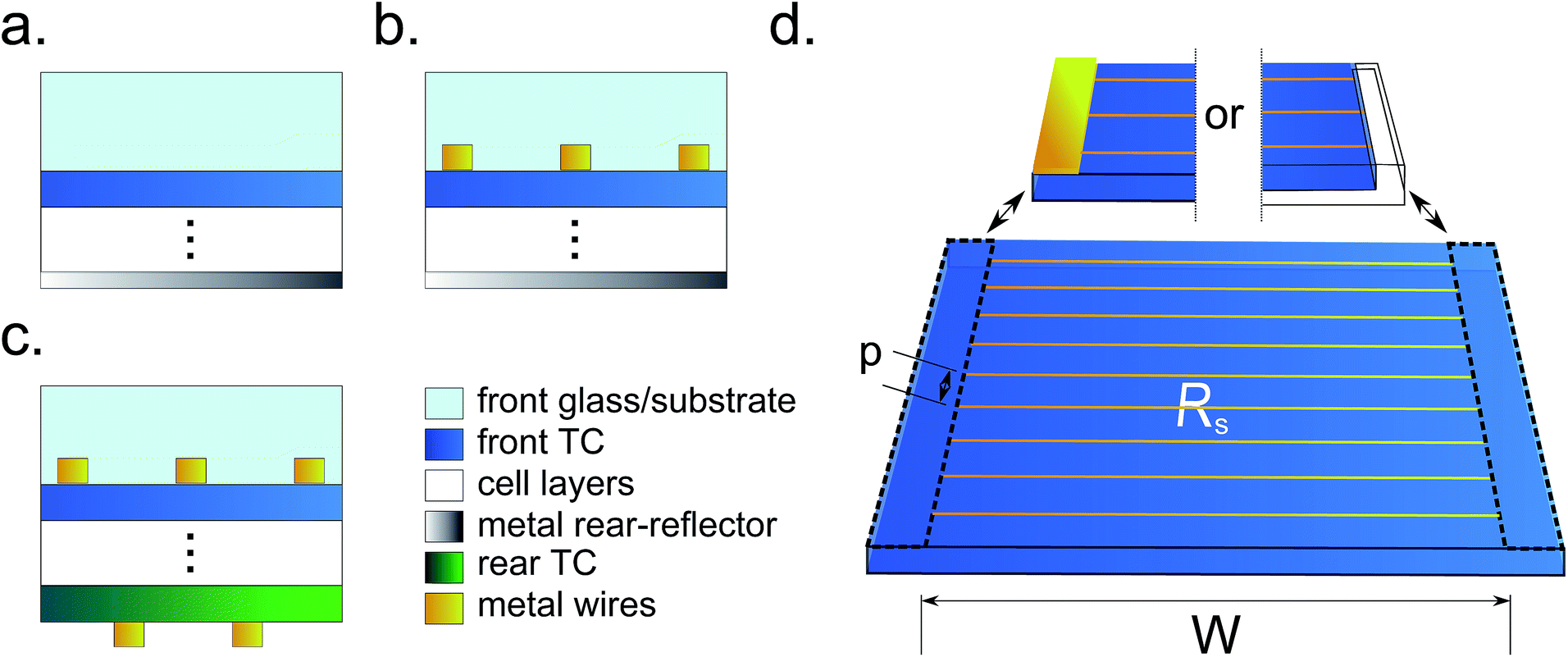 | ||
| Fig. 1 (a–c) Cross-sections of three basic cell types: (a) single cell with a bare front-side TC (b) single cell with metal wires inset into the front glass/substrate and (c) a semi-transparent cell with metallized front and rear TCs, such as might be used as the top-cell in a 4-terminal tandem device. (d) Schematic of a metallized TC in which the cell width W is defined as the distance between bus-bars (standard Si-type module), the scribed interconnect regions (monolithic thin-film module) or cell contacts (lab cell). | ||
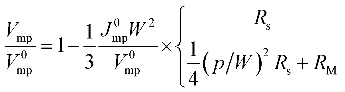
Whether or not a transparent conductor is metallized, the optimal balance between its sheet resistance and transparency is determined by the joint effect of these properties on its cell's efficiency. To model this effect we will at first consider the top electrode on a stand-alone cell (Fig. 1(a and b)). To a good approximation26 the sheet resistance of such an electrode affects the cell output voltage, whilst its transparency affects the current. Eqn (1a) given below is for the reduction in voltage Vmp/V0mp in a cell with an un-metallized or “bare” transparent conductor (Fig. 1(a)), normalized to its nominal value in an idealized cell without any ohmic loss. The second eqn (1b) for the same factor is also standard27 and applies instead to a layer with metal wires as in Fig. 1(b and d). It is derived by assuming that all the collected current flows directly through the TC to wires spaced at a period of p, before being conducted along the wires to the cell's contact, busbar or interconnect regions separated by a distance W (see Fig. 1(d)):
 | (1a,b) |
 . In general this represents a significant improvement as the value RM can be made very small at an almost negligible cost to transparency – for example, mesoscopic copper wires with p/w = 100 and h = 1 μm will shade just 1% of the incident radiation at RM ≈ 2 Ω sq−1. By comparison, a typical TC with comparable sheet resistance would block around 20% of the incoming light or more.2 Within fabrication constraints the wires can be made taller to reduce RM at no cost to transparency, which is therefore equivalent to reducing the metal's intrinsic resistivity ρ. Meanwhile, the factor (p/W)2 in the effective sheet resistance can drastically reduce the impact of the TC's sheet resistance Rs in a metallized electrode when the wires are spaced close together, allowing for the use of highly transparent TCs with a larger sheet resistance than would otherwise be optimal. For this purpose the wire width w must be made as small as possible so that the wires do not incur a large shading loss when closely spaced.
The W2 scaling of ohmic loss with cell width makes this parameter an important determinant of sheet resistance requirements. In a monolithic thin-film module the tendency to make W smaller in order to reduce ohmic loss is countered by the necessary presence of interconnect regions, which represent undesirable dead space and should therefore be spaced far apart. Technological limits on the width of these interconnect regions set the balance at roughly W ≈ 1 cm, which leads to a required sheet resistance without metallization of about 10 Ω sq−1.9 This well-known figure is visible in Fig. 2 where we have plotted the maximum allowable sheet resistance in order to keep losses under 5%, versus cell width, assuming a bare transparent conductor with perfect transparency (blue dotted line). The same quantity is also plotted for a metallized layer, but this time including the effect of wire shading in the 5% loss (red solid line). For longer cell widths metallization relaxes the required sheet resistances by a large amount, indeed by over two orders of magnitude at W = 1 cm. Another important point regarding W is that whereas for a bare electrode the cell length affects the voltage loss through Rs, in a metallized electrode the variation in loss with length scales with RM, tying the optimal value for W to the wire height. Taller wires with their reduced RM will allow for larger values of the cell width, which can reduce the negative impact of interconnect dead-space and thereby enhance module efficiency (see ESI† for quantitative estimates).
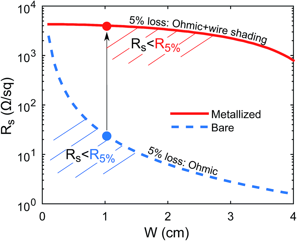 | ||
| Fig. 2 Sheet resistance requirements as a function of the contact/interconnect separation W for a bare TC (dotted, blue) and metallized TC (solid, red) assuming 5% efficiency loss in a cell with J0mp/V0mp = 22 kΩ−1 cm−2. Losses were calculated assuming 100% TC transparency, and therefore include only ohmic dissipation for the bare layer, and ohmic dissipation plus wire shading for the metallized layer. | ||
Just as the ohmic losses discussed above incur a reduction in cell voltage Vmp/V0mp, the effect of non-ideal transparency is to reduce the cell's nominal photocurrent J0mp by a factor  from the wire shading, and further by a factor T due to the TC's transparency. At the module level, current is again reduced by a factor
  due to the interconnect space discussed above, where s is the interconnection width. Taken together the ohmic and current losses reduce power generation efficiency by a factor of Jmp/J0mp × Vmp/V0mp, or
 | (2a,b) |
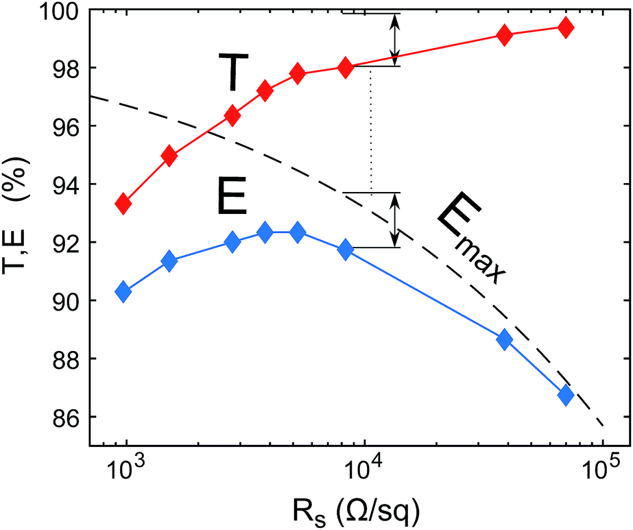 | ||
| Fig. 3 Experimental transparency and sheet resistance values for the carbon nanotube layers of ref. 28 (red upper series) and the corresponding efficiency factors (blue lower series) after including metallization with w = 30 μm and W = 1 cm. Each point lies below the maximal efficiency factor Emax (dotted) by a distance proportional to (1 − T). | ||
In Fig. 4 we have used published Rs,T data28,30–38 to compute efficiency factors for a variety of TC technologies with and without a metal grid.29 The cell parameters are taken to correspond roughly with a state-of-the-art perovskite cell, so that J0mp/V0mp = 25 mA cm−2/1.1 V = 22 kΩ−1 cm−2, and we use an interconnection width of s = 200 μm.9 The shaded regions in Fig. 4 denote unphysical efficiency factors defined by E > Emax, and each data point is situated at the coordinates (Rs,TEmax). This comparison reveals that the wire width plays a deciding role in determining which TC technologies give acceptable performance in a solar device. For moderate wire widths of w = 30 μm (Fig. 4(a)), corresponding roughly to the capabilities of industrial screen printing, sheet resistances up to a few hundreds of Ohms per square remain competitive, and in that region the competition between technologies is fairly close. For smaller wires of width w = 5 μm the playing field is almost completely leveled, and high performance can be obtained with sheet resistances as large as several thousands of Ohms per square (Fig. 4(b)). By contrast, without metallization electrode performance drops off rapidly with increasing sheet resistance and the best candidates lie in the region of 10–50 Ω sq−1 (Fig. 4(c)). Comparing the best performers in each case we find that a relative efficiency improvement of approximately 5% can be expected in moving from bare to metallized electrodes. It is also clear that transparency becomes the primary measure of TC quality when smaller wire widths are available. This means that emerging TC technologies such as carbon-nanotubes, which are generally regarded as having unsuitably high sheet resistance for solar applications, can give competitive and even superior performance with the use of narrow-width metallization due to their ultra-high transparency.39 Significantly, nearly all of the data in Fig. 4(a and b) trends steeply upwards with increasing sheet resistance, suggesting that in most cases the optimal transparency for these technologies (when augmented with a metal grid) has yet to be demonstrated.
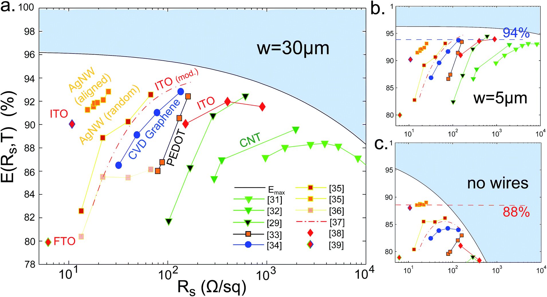 | ||
| Fig. 4 Plots of the efficiency factor E calculated using experimental (Rs,T) data from the literature.29 The wire widths are 30 μm in (a), 5 μm in (b), whereas (c) corresponds to a bare electrode. In each case the interconnect width is set to 200 μm and for (a) and (b) the wire height is 3 μm. | ||
The efficiency factors defined in (2) were introduced for the top electrode of a stand-alone cell, but a similar strategy can be pursued to model the performance of TCs in tandem cells with only slightly different equations. We include such an analysis in the ESI.†
3 Figures of merit for solar cells
To ease comparisons TCs are often ranked in terms of a figure of merit which is a simple function of sheet resistance and transparency. The most widely used is the DC to optical conductivity ratio40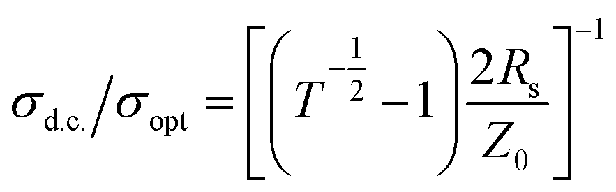 | (3) |
| ΦH = Tq/Rs | (4) |
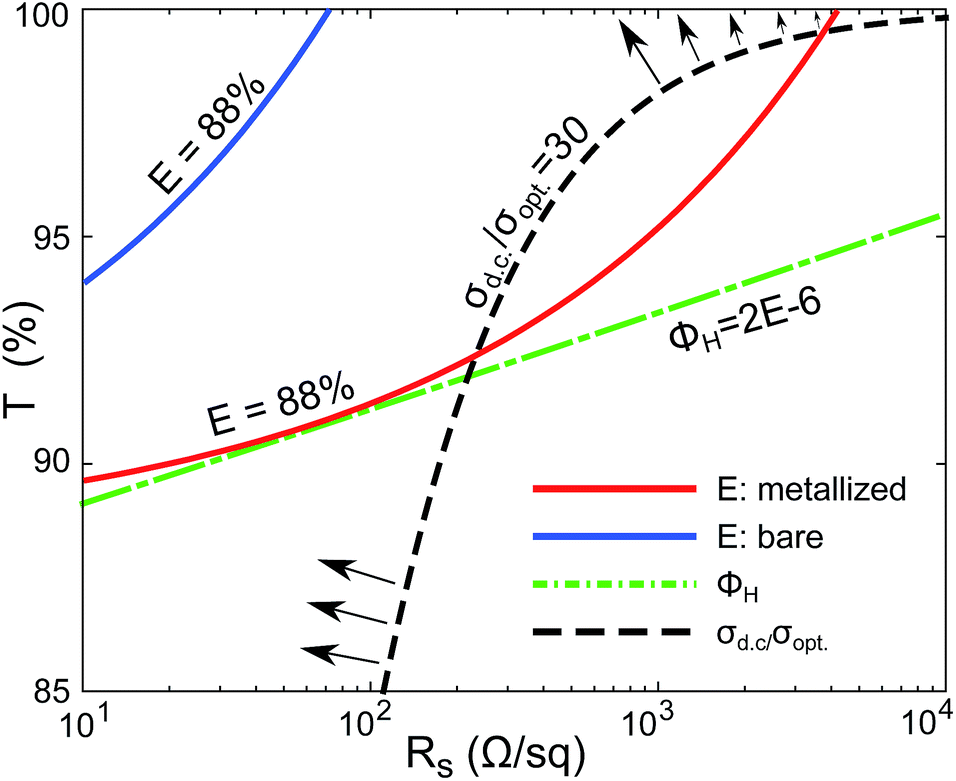 | ||
| Fig. 5 Level curves of the d.c. to optical conductivity ratio (black dashed) and Haacke's function (green dot-dash), as compared to contours of equal loss factor computed using eqn (5) (blue) and (6) (red). For the bare loss factor we have set s = 200 μm, the wire width w = 30 μm and in both cases J0mp/V0mp = 22 kΩ−1 cm−2. Normally-oriented arrows on the conductivity ratio point in the direction of maximum “improvement”. | ||
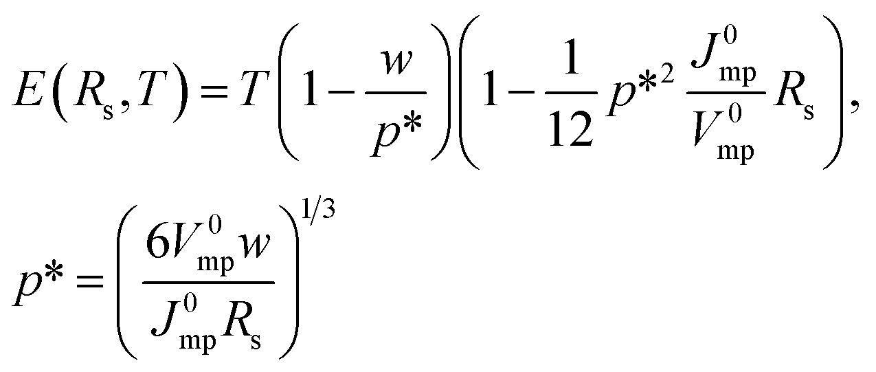
For a bare electrode eqn (2a) can readily be put in the form of a simple figure of merit as the optimization problem for W has a simple analytic solution. This gives the expression:
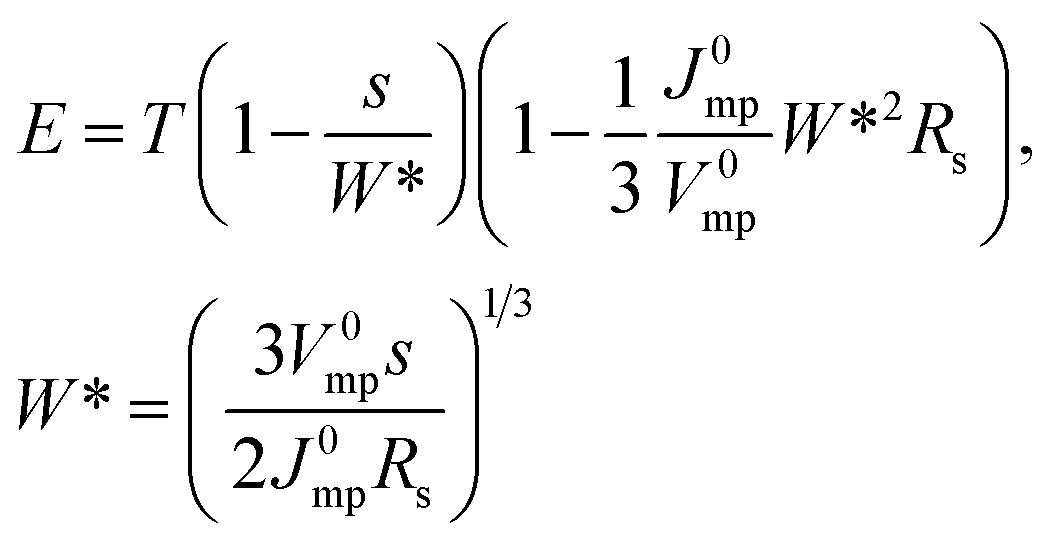 | (5) |
 | (6) |
4 Conclusions
Metallization relieves the burden on a transparent conductor's sheet resistance, leveling the competition between technologies and allowing for other factors such as material compatibility or ease of processing to take precedence. Whenever it is possible to incorporate a narrow metallic grid (w < 30 μm), the requirements for a transparent conductor shift dramatically towards achieving ultra-high transparency (>95%). Wire widths in the range of 20–30 μm already relax the conventional sheet resistance requirement of 10 Ω sq−1 by more than an order of magnitude, encompassing a wide range of emerging technologies, whilst widths approaching 5 μm will allow for several thousands of ohms per square in the transparent layer. Furthermore, we have shown that metallized transparent layers generally exceed the performance of the best bare transparent conductors due to a combined reduction of losses at the cell and module level. Narrow-width metallization therefore provides a clear route for approaching ideal electrode performance in thin-film solar cells. These findings demonstrate the potential for scalable methods of incorporating thin metal wires into cell substrates to disrupt the transparent conductor landscape.For sensitive cell architectures embedding of the wires may be necessary to avoid drastic nonuniformities, and this is likely to be simpler for flexible polymer substrates than for glass. However even in the latter case one may look to the literature of microfluidics where the problem of structuring glass has received considerable attention,44,45 or to well-established sol–gel techniques12,13 for imprinting patterns onto glass. Once embedded, these metal wires could be made very much taller than otherwise in order to accommodate larger cell widths, providing a reduction in module dead-space. Electrodes which are naturally exposed, such as the rear electrode in a perovskite four-terminal tandem device, can be easily metallized and researchers should be aware that this obviates the standard requirement of 10 Ω sq−1.
As a figure of merit for solar cells we have shown that the widely used optical to d.c. conductivity ratio exhibits highly unphysical biases in the low and high Rs regimes, and particularly overestimates the value of having low sheet resistance, even for un-metallized electrodes. By modeling their expected impact on solar cell efficiency, we have suggested new figures of merit for transparent conductors with clear relevance for solar applications and a sound physical basis.
Acknowledgements
The authors gratefully acknowledge The Duong for his contribution of the TCO film data appearing in Fig. 4, and Niraj Lal for useful discussions. KC acknowledges support from the Australian Research Council Future Fellowship Scheme. This work has been supported by the Australian Government through the Australian Renewable Energy Agency (ARENA). Responsibility for the views, information or advice expressed herein is not accepted by the Australian Government.References
- D. S. Hecht, L. Hu and G. Irvin, Adv. Mater., 2011, 23, 1482–1513 CrossRef CAS PubMed.
- K. Ellmer, Nat. Photonics, 2012, 6, 809–817 CrossRef CAS.
- M. Layani, A. Kamyshny and S. Magdassi, Nanoscale, 2014, 6, 5581–5591 RSC.
- H. J. Snaith, J. Phys. Chem. Lett., 2013, 4, 3623–3630 CrossRef CAS.
- M. A. Green, A. Ho-Baillie and H. J. Snaith, Nat. Photonics, 2014, 8, 506–514 CrossRef CAS.
- N. Lal, T. White and K. Catchpole, Journal of Photovoltaics, 2014, 4, 1380–1386 CrossRef.
- C. D. Bailie, M. G. Christoforo, J. P. Mailoa, A. R. Bowring, E. L. Unger, W. H. Nguyen, J. Burschka, N. Pellet, J. Z. Lee, M. Gratzel, R. Noufi, T. Buonassisi, A. Salleo and M. D. McGehee, Energy Environ. Sci., 2015, 8, 956–963 CAS.
- P. Löper, S.-J. Moon, S. Martín de Nicolas, B. Niesen, M. Ledinsky, S. Nicolay, J. Bailat, J.-H. Yum, S. De Wolf and C. Ballif, Phys. Chem. Chem. Phys., 2015, 17, 1619–1629 RSC.
- M. W. Rowell and M. D. McGehee, Energy Environ. Sci., 2011, 4, 131–134 CAS.
- J. Wennerberg, J. Kessler and L. Stolt, Sol. Energy Mater. Sol. Cells, 2001, 67, 59–65 CrossRef CAS.
- T. Duong, N. Lal, D. Grant, D. Jacobs, P. Zheng, S. Rahman, H. Shen, M. Stocks, A. Blakers, K. Weber, T. P. White and K. R. Catchpole, IEEE Journal of Photovoltaics, 2016, PP, 1–9 CrossRef.
- C. Marzolin, S. P. Smith, M. Prentiss and G. M. Whitesides, Adv. Mater., 1998, 10, 571–574 CrossRef CAS.
- O. J. A. Schueller, G. M. Whitesides, J. A. Rogers, M. Meier and A. Dodabalapur, Appl. Opt., 1999, 38, 5799–5802 CrossRef CAS PubMed.
- K. Tvingstedt and O. Inganäs, Adv. Mater., 2007, 19, 2893–2897 CrossRef CAS.
- M. Ju, Y.-J. Lee, J. Lee, B. Kim, K. Ryu, K. Choi, K. Song, K. Lee, C. Han, Y. Jo and J. Yi, Sol. Energy Mater. Sol. Cells, 2012, 100, 204–208 CrossRef CAS.
- H. Sirringhaus, T. Kawase, R. H. Friend, T. Shimoda, M. Inbasekaran, W. Wu and E. P. Woo, Science, 2000, 290, 2123–2126 CrossRef CAS PubMed.
- Z. Li, P.-C. Hsiao, W. Zhang, R. Chen, Y. Yao, P. Papet and A. Lennon, Energy Procedia, 2015, 67, 76–83 CrossRef CAS.
- A. Lorenz, A. Senne, J. Rohde, S. Kroh, M. Wittenberg, K. Kruger, F. Clement and D. Biro, Energy Procedia, 2015, 67, 126–137 CrossRef CAS.
- S. Thibert, D. Chaussy, D. Beneventi, N. Reverdy-Bruas, J. Jourdan, B. Bechevet and S. Mialon, 38th Photovoltaic Specialists Conference, 2012, pp. 2266–2270 Search PubMed.
- S. H. Ahn and L. J. Guo, Adv. Mater., 2008, 20, 2044–2049 CrossRef CAS.
- A. Kumar and G. M. Whitesides, Appl. Phys. Lett., 1993, 63, 2002–2004 CrossRef CAS.
- Y.-L. Loo, R. L. Willett, K. W. Baldwin and J. A. Rogers, Appl. Phys. Lett., 2002, 81, 562–564 CrossRef CAS.
- P.-C. Hsu, S. Wang, H. Wu, V. K. Narasimhan, D. Kong, H. Ryoung Lee and Y. Cui, Nat. Commun., 2013, 4, 2522 Search PubMed.
- J. Zou, H.-L. Yip, S. K. Hau and A. K.-Y. Jen, Appl. Phys. Lett., 2010, 96, 203301 CrossRef.
- Y. Zhu, Z. Sun, Z. Yan, Z. Jin and J. M. Tour, ACS Nano, 2011, 5, 6472–6479 CrossRef CAS PubMed.
- G. T. Koishiyev and J. R. Sites, Sol. Energy Mater. Sol. Cells, 2009, 93, 350–354 CrossRef CAS.
- M. Green, Centre Photovoltaic Devices & Systems, Silicon Solar Cells: Advanced Principles & Practice, 1995, p. 366 Search PubMed.
- H.-Z. Geng, K. K. Kim, K. P. So, Y. S. Lee, Y. Chang and Y. H. Lee, J. Am. Chem. Soc., 2007, 129, 7758–7759 CrossRef CAS PubMed.
- In all figures we have used transparency values reported at 550 nm, with the exception of the transparent oxide films (ITO and FTO) which generally exhibit a considerable variation in transmission with wavelength. For ITO and FTO each transmittance was weighted with the AM1.5g spectrum. For the other technologies full spectral data was not available.
- V. Scardaci, R. Coull and J. N. Coleman, Appl. Phys. Lett., 2010, 97, 5–8 CrossRef.
- J. Li, L. Hu, L. Wang, Y. Zhou, G. Grüner and T. J. Marks, Nano Lett., 2006, 6, 2472–2477 CrossRef CAS PubMed.
- J. E. McCarthy, C. a. Hanley, L. J. Brennan, V. G. Lambertini and Y. K. Gun'ko, J. Mater. Chem. C, 2014, 2, 764–770 RSC.
- S. Bae, H. Kim, Y. Lee, X. Xu, J.-S. Park, Y. Zheng, J. Balakrishnan, T. Lei, H. R. Kim, Y. I. Song, Y.-J. Kim, K. S. Kim, B. Ozyilmaz, J.-H. Ahn, B. H. Hong and S. Iijima, Nat. Nanotechnol., 2010, 5, 574–578 CrossRef CAS PubMed.
- S. Kang, T. Kim, S. Cho, Y. Lee, A. Choe, B. Walker, S.-J. Ko, J. Y. Kim and H. Ko, Nano Lett., 2015, 15, 7933–7942 CrossRef CAS PubMed.
- Silver nanowire data34 (random array) with the efficiency factor calculated without metallization (i.e. for a bare electrode), included for comparison.
- For this series we have modelled the transmission through ITO layers of varying thickness using the Beer-Lambert formula for absorption, taking the extinction coefficient from ref. 46 and neglecting reflection.
- In-house measurements of RF-sputtered ITO deposited at room temperature (see ref. 11 for further details).
- In-house measurements of commercial samples of ITO (Sigma Aldrich 578274, t≈120 nm on glass) and FTO (Dyesol TEC7, t≈650 nm on glass). As the reflectance of these thin-films can vary widely we have elected to include only absorption in the transparency data, so that T = 1−A, making these values an upper estimate.
- We note that a significant loss in voltage or collection efficiency may result if the mobility of the underlying active layer is not sufficient to ensure a smooth passage for carriers to the individual tubes (for CNT layers) or nanowires (AgNW electrodes), an issue which may arise in certain organic semiconductors.
- S. De and J. N. Coleman, MRS Bull., 2011, 36, 774–781 CrossRef CAS.
- G. Haacke, J. Appl. Phys., 1976, 47, 4086–4089 CrossRef CAS.
- K. Ramanathan, J. Keane and R. Noufi, Conference Record of the Thirty-first IEEE Photovoltaic Specialists Conference, 2005, pp. 195–198 Search PubMed.
- X. Wu, R. G. Dhere, D. S. Albin, T. A. Gessert, C. DeHart, J. C. Keane, A. Duda, T. J. Coutts, S. Asher, D. H. Levi and et al., in High-Efficiency CTO/ZTO/CdS/CdTe Polycrystalline Thin-Film Solar Cells: Preprint, 2001 Search PubMed.
- M. Stjernström and J. Roeraade, J. Micromech. Microeng., 1999, 8, 33–38 CrossRef.
- C. Iliescu, F. E. H. Tay and J. Miao, Sens. Actuators, A, 2007, 133, 395–400 CrossRef CAS.
- Z. C. Holman, M. Filipič, A. Descoeudres, S. DeWolf, F. Smole, M. Topič and C. Ballif, J. Appl. Phys., 2013, 113, 013107 CrossRef.
Footnote |
| † Electronic supplementary information (ESI) available. See DOI: 10.1039/c6ta01670g |
| This journal is © The Royal Society of Chemistry 2016 |