
 Open Access Article
 This Open Access Article is licensed under a
 Creative Commons Attribution 3.0 Unported Licence
Synthesis, characterization and DFT studies of zinc-doped copper oxide nanocrystals for gas sensing applications†
V.
Cretu
 a,
V.
Postica
a,
A. K.
Mishra
b,
M.
Hoppe
c,
I.
Tiginyanu
a,
Y. K.
Mishra
c,
L.
Chow
d,
Nora H.
de Leeuw
*be,
R.
Adelung
c and
O.
Lupan
*ac
a,
V.
Postica
a,
A. K.
Mishra
b,
M.
Hoppe
c,
I.
Tiginyanu
a,
Y. K.
Mishra
c,
L.
Chow
d,
Nora H.
de Leeuw
*be,
R.
Adelung
c and
O.
Lupan
*ac
aDepartment of Microelectronics and Biomedical Engineering, Technical University of Moldova, 168 Stefan cel Mare Av., MD-2004 Chisinau, Republic of Moldova
bDepartment of Chemistry, University College London, 20 Gordon Street, London WC1H 0AJ, UK. E-mail: n.h.deleeuw@ucl.ac.uk; deleeuwn@cardiff.ac.uk; abhishek.mishra@ucl.ac.uk
cFaculty of Engineering, Institute for Materials Science, Christian-Albrechts Universität zu Kiel, Kaiserstr. 2, D-24143, Kiel, Germany. E-mail: ra@tf.uni-kiel.de; ollu@tf.uni-kiel.de; lupanoleg@yahoo.com
dDepartment of Physics, University of Central Florida, Orlando, FL 32816-2385, USA
eSchool of Chemistry, Cardiff University, Main Building, Park Place, Cardiff CF10 3AT, UK
First published on 7th April 2016
Abstract
Due to their unique properties, p-type copper oxide nanostructures have demonstrated promising potential for various applications, especially for the detection of ethanol vapour and other volatile organic compounds (VOCs). In this work a simple and cost-effective synthesis from chemical solutions (SCS) at low temperatures (≤80 °C) and rapid thermal annealing (RTA) process were used to grow zinc-doped copper oxide (ZnxCu1−xOy) nanostructures. The structural, morphological, vibrational, chemical, electronic and sensorial characteristics of ZnxCu1−xOy nanocrystallite layers obtained by using such an efficient approach based on both, the SCS and RTA processes, have been studied. The investigations demonstrated the possibility to tune sensitivity from VOC to H2, as well as an improved response and high selectivity with respect to hydrogen gas for ZnxCu1−xOy nano-crystalline thin films with x = 0.03. Density functional theory calculations showed that the charge transfer together with changes in the Fermi level facilitate H2 gas sensing, which is further enhanced by Zn doping. Hydrogen gas sensing with a high response and selectivity using p-type hybrid semiconductor nanostructures has been reported. An improved stability in humid air was observed by exposure of doped samples to rapid thermal annealing process for the first time. The experimental and calculation results provide an alternative to sensitive and selective detection of ethanol and hydrogen gases, which would be of particular benefit in the area of public security, industrial and environmental applications.
Introduction
Hydrogen is widely used in industries, as a power source in aerospace, for metal sintering and annealing, in research laboratories, biomedical systems, automotive and transportation equipment, etc.1–8 Therefore, the reliable, selective and fast detection of hydrogen gas leaks appears to be the strict necessity for preventing the accumulation of hydrogen in air (4% H2).6 In this context nano- and microstructures of p-type materials and especially the n-type semiconducting oxides have been intensively investigated over the past few decades due to their remarkable gas sensing properties, and importance for fundamental research and applied technologies.9–12 Due to their unique properties and specific gas sensing mechanism, p-type copper oxide nanostructures have demonstrated promising potentials in various gas sensing applications, especially in detection of ethanol vapour and other volatile organic compounds (VOCs), like benzene, acetone and toluene, etc.13–17 Copper oxide semiconductors and their derivatives are excellent candidates for the fabrication of low-cost p-type nanosensors due to high abundance of copper in nature,18 simple synthesis and nanointegration methods.19However, most of the reported studies on gas sensing properties of copper oxides with different types of morphologies have demonstrated selective ethanol or acetone vapour sensing14,20,21 and only a few reports reveal the selectivity and response with respect to hydrogen gas.17,22–24 In this context, the change of chemical and physical properties by doping of foreign elements is an important and efficient way to further control the gas sensing characteristics of semiconducting oxides such as sensitivity, response and recovery times, as well as selectivity.16 From the existing literature, it is difficult to find any study which demonstrates the p-type nanomaterials based hydrogen gas sensing with high response/selectivity characteristics.
In this work, the synthesis of zinc-doped copper oxides, ZnxCu1−xOy, nano-crystalline films by a synthesis from chemical solutions (SCS) method and rapid thermal annealing (RTA) process has been developed. We report on the details of the growth process, phase analysis, chemical composition, vibrational and sensorial performances of the functional copper oxide treated by conventional thermal annealing (TA) in electrical furnace and by RTA in air. A mixed phase of CuO:Zn/Cu2O:Zn in samples TA-treated at 400–450 °C for 30 min and RTA-treated at 525 °C for 60 s was detected by XRD, EDX and micro-Raman measurements. An enhanced H2 gas response and improved stability to humidity of RTA-treated samples with high Zn content was demonstrated by gas sensing measurements. Based on the ionosorption model and density functional theory (DFT) calculations, the gas sensing mechanism was proposed.
Experimental
Pure copper oxides, CuxOy, and zinc-doped copper oxides, ZnxCu1−xOy, nano-crystalline films were grown on glass substrates (microscope slides 76 mm × 25 mm × 1 mm) via SCS. The procedure of substrate cleaning was described in our previous work.25 The substrate surface was sensitized with SnCl2/HCl solution.26,27 For SCS deposition process the substrates were immersed vertically in the solutions using a microcontroller based system to grow Cu2O nanostructured films with desired thickness, by controlling the number of cycles and time of substrate immersion in the solutions. The deposition system includes a home-made robot arm, controlled by a microcontroller through a graphical user interface (GUI), with the possibility to send commands and set parameters through a wireless module. A typical schematic for our set-up with related description is represented in Fig. S1.† The main advantage of the presented system is the exclusion of errors due to human factors which actually leads to high reproducibility of the samples and commodity in synthesis process. Wireless communication allows operation control out of fume hood in case of work with toxic chemicals or in the case of emanation of harmful gases after chemical reactions in the deposition process.The aqueous copper-complex solution, as cation precursor, comprises a mixture of 1 M copper sulfate (CuSO4·5H2O) and 1 M sodium thiosulfate (Na2S2O3·5H2O). In order to prepare the Zn-doped nano-crystalline films, two new baths, one containing Cu+ ions and the other filled with only deionized (DI) water, were included in the growth system. The Zn doping of Cu2O nanostructured films was achieved by adding ZnSO4·7H2O in the copper complex solution corresponding to the necessary concentration of Zn in nanostructured films. For doping concentrations (#1) – 1.5 mM, (#2) – 4 mM and (#3) – 6 mM of zinc ions were added in complex solutions, thus the Zn doping level from 0 to 3 wt% Zn was varied according to EDX results. Deionized water (resistivity 18.2 MΩ cm) was used as solvent. NH4OH was added to the initial solution to control the complex solution and the value of pH was 10. The copper complex solution was diluted with DI water to obtain 0.1 M copper concentration and was maintained at room temperature during the film deposition. The anionic precursor solution comprises sodium hydroxide (NaOH) diluted with DI water to obtain 2 M and was maintained at 80 °C during the film deposition. All chemicals were of reagent grade. After deposition, the nano-crystalline films were rinsed well with DI water, and then dried for 5 min at 150 °C in air flux. The global reaction of copper complex solution preparation for Cu2O nano-crystalline films deposition was described in previous works.11,28 A single deposition cycle of a Cu2O nano-crystalline film is described by the following two steps: (1) immersion of substrate in the hot (80 °C) alkali solution for the adsorption of the (OH)− ions on the glass substrate; (2) dipping this substrate in the thiosulfatocuprate(I) for reaction of the copper ions and zinc ions with adsorbed (OH)−. This is one cycle of the ion layers adsorption and reaction processes in our method. The copper ions are formed by the dissociation equilibrium.11,28
Equation of Cu2O forming is represented by:11,28
| 2Cu+ + 2OH− → 2CuOH → Cu2O + H2O | (1) |
Post-growth treatment is an important factor to increase the crystallinity of nanostructured oxide films after chemical synthesis.11,28 In this work, the as-grown films were subjected to two types of post-growth treatments in air, namely conventional thermal annealing (TA) in an electrical furnace and rapid thermal annealing (RTA).29 Typical schematic temperature profiles for TA and RTA – treatments at 450 °C and 525 °C are represented in Fig. S2a and b,† respectively. A typical schematic diagram of our RTA set-up is represented in Fig. S2c.†
The samples morphology was investigated by using scanning electron microscopy (SEM) REM-ZEISS (at 7 kV). The chemical composition of the SCS samples was examined by EDX spectroscopy. Concentrations of Zn dopants in copper oxide layers were noted and found as (#1 or c1) – 1.9 wt% Zn, (#2 or c2) – 2.7 wt% Zn; (#3 or c3) – 3.0 wt% Zn in the case of RTA treated samples and (#1 or c1) – 1.9 wt% Zn, (#2 or c2) – 2.4 wt% Zn; (#3 or c3) – 2.8 wt% Zn in the case of TA treated specimens. Crystallographic data were obtained from X-ray powder diffraction (XRD) investigations using a Seifert XRD3000 PTS instrument operating at 40 kV and 40 mA, with CuKα1 radiation, λ = 1.54184 Å. Secondary ion mass spectroscopy (SIMS) studies were performed with a Physical Electronics ADEPT 1010 quadrupole analyzer. The primary beam (25 nA) was applied to a 300 μm by 300 μm area, with the detection of negative secondary ions from an area of 100 μm by 100 μm at the centre. Technical information of the experiment can be found in our earlier reports.7,30,31 Micro-Raman studies were performed at room temperature with a WITec alpha 300 RA system in a backscattering configuration. The Nd-YAG laser power was less than 4 mW at the sample.7 The investigated sample sizes were 5 mm in width and few cm in length. Each measurement was performed on an individual sample and re-checked on several ones from the same set. Electrical studies were carried out using the two-point probe method at room temperature. Gas sensing properties were evaluated according to the previous reports.8,32,33
Different values of relative humidity (RH) were generated using a bubbling system. Air was passed through water and then was continuously injected into the chamber to create the necessary RH value. The humidity was continuously monitored by a standard hygrometer. More details can be found in previous works.8,32,33
Computational methodology
Density functional theory (DFT) calculations were realized by the Vienna Ab initio Simulation Package (VASP) with a plane-wave basis set.34–37 The projector augmented wave method was certified to describe the interaction between electrons and ions,38 and the non-local exchange correlation energy was considered using the Perdew–Burke–Ernzerhof functional.39,40 The Hubbard model was involved to treat strong correlations within the DFT + U method in the Dudarev formalism.41Recently, we have determined a value of U that can efficiently describe both copper I and II oxides42 and this effective U value of 7 eV was chosen for the localized 3d electrons of Cu, whereas U = 6 eV was taken for the Zn-3d electrons.43 The atomic structures were relaxed using the tetrahedron method with Bloch correction as implemented in VASP and the positions of all atoms in the cell were fully relaxed until the atomic forces on each ion were less than 0.01 eV Å−1. To model Zn doping, we have used our earlier bulk and surface models of CuO and Cu2O.42,44 We have further used the implementation of the DFT-D2 approach described by Grimme45 to account for long-range dispersion forces.
We sampled the (1 × 1) surface cells with a 5 × 5 × 1 Monkhorst–Pack46k-point mesh, while (2 × 1) supercells were modelled with 2 × 4 × 1 k-point mesh. Electronic density-of-states (DOS) of (2 × 1) supercells were calculated using a higher 4 × 8 × 1 k-point mesh with a tetrahedron smearing parameter of 0.1 eV and a Self-Consistent-Field (SCF) convergence criterion of 1 × 10⁻⁶ eV per unit cell.
The binding energy of H2 molecule was calculated from the relation:
| Eads = ECuO/Cu2O–Zn+H2 − (ECuO/Cu2O–Zn + EH2) | (2) |
Results and discussion
Morphological SEM and compositional EDX studies
To investigate the surface morphology of SCS grown ZnxCu1−xOy nano-crystalline films, SEM was used. The corresponding images are shown in Fig. 1 and S3.† In general, the nano-crystalline layers are homogeneously and continuously covering the glass substrates (see Fig. 1 and S3†).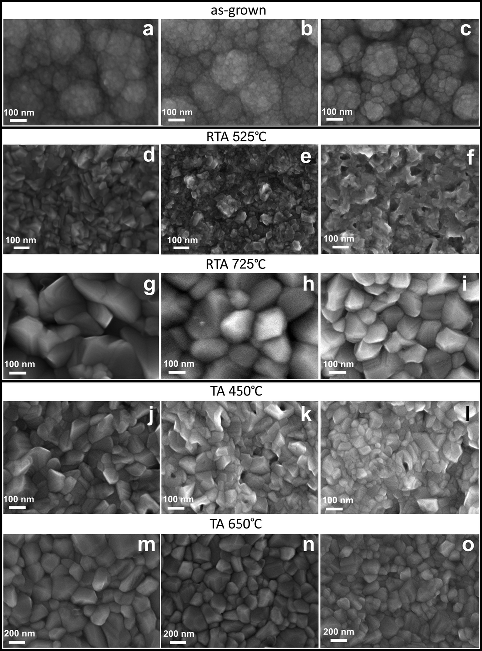 | ||
| Fig. 1 SEM images of zinc-doped copper oxide nano-crystalline films: as-grown with zinc ions concentration of (a) – Zn(1); (b) – Zn(2); (c) – Zn(3); RTA treated at 525 °C for 60 s with zinc concentration (d) – Zn(1); (e) – Zn(2); (f) – Zn(3); RTA treated at 725 °C for 60 s with zinc concentration (g) – Zn(1); (h) – Zn(2); (i) – Zn(3); TA treated at 450 °C for 30 min with zinc concentration (j) – Zn(1); (k) – Zn(2); (l) – Zn(3); TA treated at 650 °C for 30 min with zinc ions concentration (m) – Zn(1); (n) – Zn(2); (o) – Zn(3). | ||
Large islands layers are difficult to see in the sintered films formed from well-packed nanocrystallites of copper oxides covering completely the whole substrate. Typical SEM images of the as-grown films are presented in Fig. 1a–c for Zn-doped copper oxide layers with concentrations (#1 or c1), (#2 or c2) and (#3 or c3), respectively. SEM of undoped CuO–Cu2O can be found in our recent work.13 The film thickness was measured by cross-sectional SEM and the typical thickness was ∼1 μm. For samples after RTA at 725 °C (noted as RTA725 in Fig. 1g–i) or after TA at 650 °C (noted as TA650, see Fig. 1m–o and S3 and S4†), relatively large particle agglomerates can be observed in contrast to films treated at lower temperatures of RTA at 525 °C (RTA525, see Fig. 1d–f) or TA at 450 °C (TA450, see Fig. 1j–l). In these samples, marked as RTA525 and TA450, the films morphology appeared most uniform and the nanoparticle size was smaller (of about 40–60 nm). The films are formed from densely packed grains of approximately pyramidal form (Fig. 1d–f and j–l).
With further rise in sintering temperature up to 650 °C (for TA treated samples), and up to 725 °C for RTA, it appears that some fusions of grain boundaries have occurred (Fig. S5†) leading to a marginal increase in particle size, of about 120–200 nm with a columnar morphology (Fig. 1g–i and m–o).49 Fig. S5† shows a low magnification TEM image of a Zn-doped copper oxide film. The film consists of accumulated nanocrystals and its thickness amounts to 1 μm. From the TEM image in Fig. S5,† it is confirmed that the CuO:Zn films are quite porous. We observed several pinholes on the CuO:Zn sample. Typical width and length of the Zn-doped CuO nanocrystals are 50 nm and 200 nm, respectively. Such columnar growth in copper oxide has been shown by Richthofen et al.,50 but Chauhan et al.49 did not observe any preferred grain elongation. The random size and projection distributions of grains, suggest the random nucleation and growth mechanism, and hence an isotropic grain growth.51
X-ray diffraction structural analysis
In all crystallized solid materials, divalent Cu surroundings are always distorted by a large Jahn–Teller effect which generally leads to square planar groups, which are more stable.52 When the Cu2+ ions are substituted by metal (Zn2+) ions in the Zn2+ doped copper oxide sample, the difference in ionic radii53,54 between Cu2+ (r = 0.071 nm) and Zn2+ (r = 0.074 nm) leads to deformation of the CuO lattice and the strain energy may cause dislocations and imperfections in the monoclinic crystal lattice. The formula (ZnxCu1−xO1−ı, for example x = 0.03) indicates that 3 wt% of Zn atoms replace the copper (Cu) atoms to maintain charge neutrality, some of the oxygen vacancies (ı = 0.03) are created in the system. Therefore, it is reasonable to suggest that due to these reasons, the doped samples could have a higher electrical conductivity.
Fig. 2a shows X-ray powder diffractograms of the as-grown Cu2O layers (curve 1) and of the RTA treated ones (RTA525, curves 2–4), where two coexisting phases (cubic Cu2O and the monoclinic CuO) are detected. The XRD patterns show peaks of both Cu2O and CuO (Fig. 2a, curves 2–4), but the majority phase is the Cu2O because the formation of CuO would be very slow on top of cuprite layers.50,55–57 The comparison of the respective peak intensity of specimens after RTA at 525 °C shows that the Cu2O amount is higher when compared to CuO layers (Fig. 2a, curves 2–4). In the XRD pattern of TA650 and RTA725 specimens, all XRD peaks are indexed completely to the CuO monoclinic symmetry54,55 (JCPDS 45-0937, as presented in Fig. 2b, curves 2–4). X-ray powder diffractograms of all samples showed the same features. The peak at 2θ = 36.4° is strongest and was indexed to the Cu2O(111) crystal plane, and other peaks at 2θ = 29.6°, 42.3°, 61.4°, 73.6° and 77.4° are also in good agreement with the diffraction pattern of the Cu2O cubic phase54,55 (JCPDS 05-0667, as presented in Fig. 2). Even if CuO peaks are weaker compared to Cu2O peaks on the sides of the strongest peak two bands at 2θ = 35.5° and 38.7° indexing to the (−111)/(002) and (111) planes (see Fig. 2a, curves 2–4) of the monoclinic CuO can be observed, respectively. The spectra modifications should be due to a removal process of the Cu2O phase on the specimens.55 The effect of rapid thermal annealing at 725 °C for 60 s on the structure of CuO layers doped with different concentrations of zinc is presented in Fig. 2b.
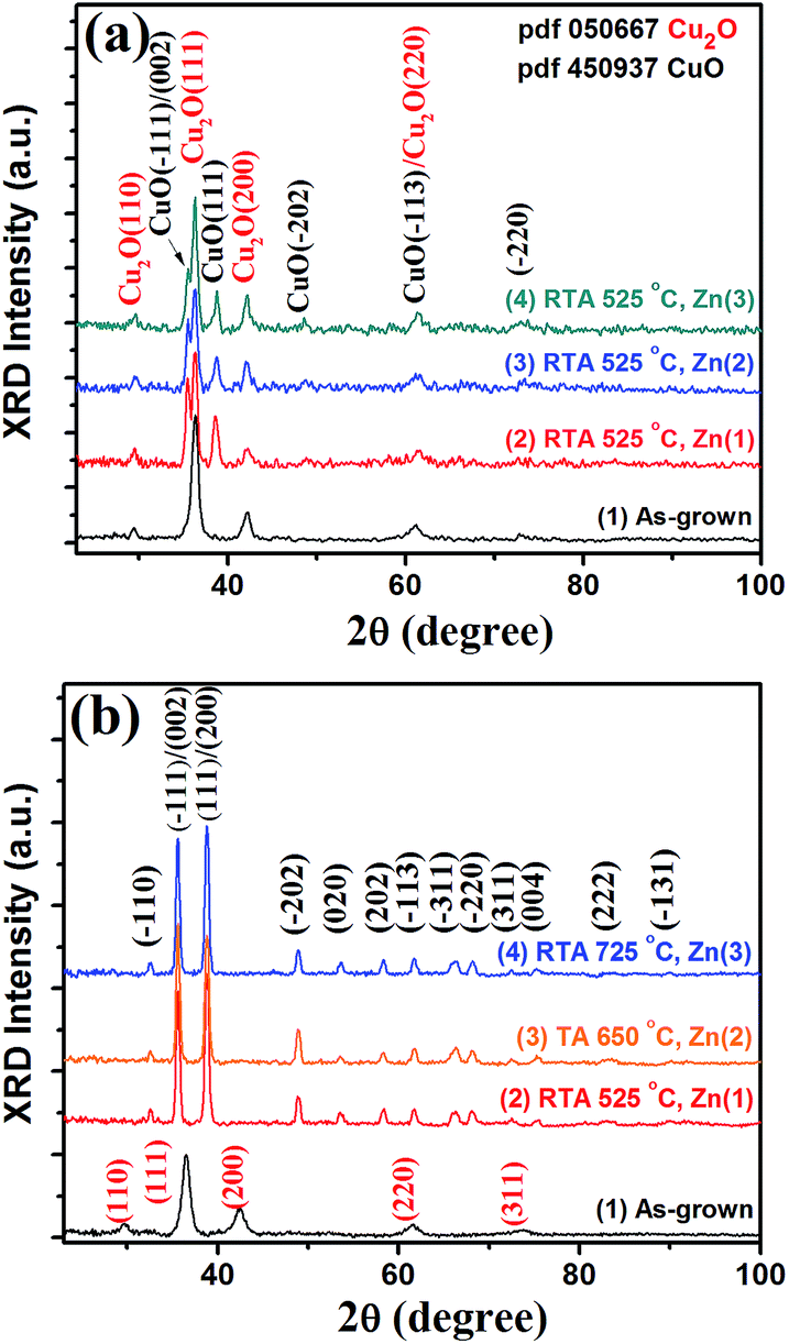 | ||
| Fig. 2 X-ray powder diffractograms of ZnxCu1−xO1−ı layers: (a) as-grown (1) and rapid thermal annealed (RTA) in air at 525 °C for 60 s. Curves 2, 3, 4 correspond to different concentrations Zn(1), Zn(2), and Zn(3) of Zn-doped copper oxide; (b) as-grown (1), RTA at 525 °C (2) and 725 °C (4) for 60 s, and thermal annealed in air at 650 °C (3) for 30 min. Curves 2, 3, 4 correspond to different concentrations Zn(1), Zn(2), and Zn(3) of Zn-doped copper oxide layers. | ||
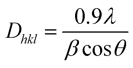
The oxide average crystallite sizes are computed from Debye–Scherer's equation from the broadening of diffraction lines (−111) and (111):54,55,58
 | (3) |
For samples marked as RTA525, the sizes of Cu2O aggregates D111 are 2.43, 2.29 and 1.09 nm, for Zn-doping concentrations 1, 2, 3, respectively. This is consistent with the corresponding SEM images of the CuO nanocrystals (see Fig. S3†). It was observed that the Cu2O aggregates increase in size with the treatment temperatures, but decrease with the doping level. For CuO, the aggregate sizes D111 are 2.43, 2.39, and 1.47 nm, for samples doped with concentrations #1, #2, and #3, respectively (sample sets TA650-treated).
The information on the structural characteristics of the CuO nano-crystalline layers were obtained by computing the strain (ε), the average crystallite size (D), as well as the dislocation density (δ) according to the relations:59,60
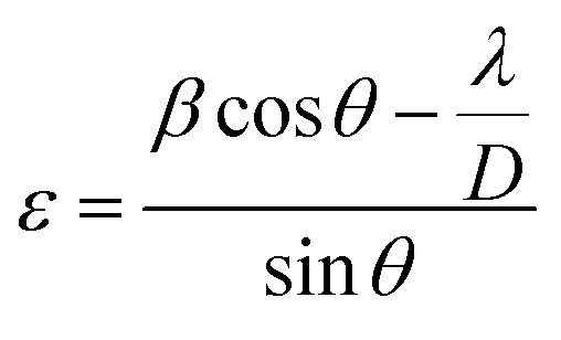 | (4) |
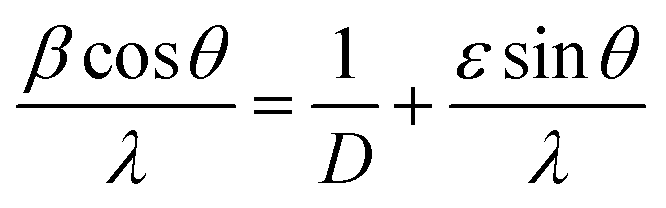 | (5) |
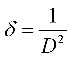 | (6) |
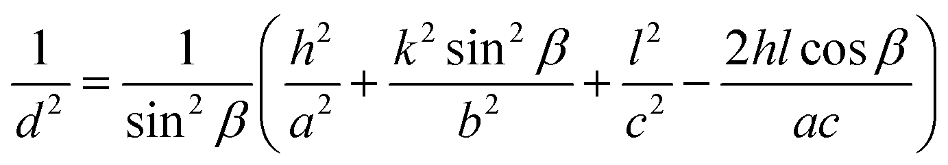
Lattice parameters (a ≠ b ≠ c, α = γ = 90° ≠ β for monoclinic structure) and the unit cell volume for the CuO layers were found by following the equations:61
 | (7) |
V = abc![[thin space (1/6-em)]](https://www.rsc.org/images/entities/char_2009.gif) sinβ sinβ | (8) |
The calculated structural parameters of the Zn-doped copper oxide thin films indicate no significant changes in values. According to the XRD results, the Zn-doped CuO samples contain no detectable impurities, but the lattice parameters slightly differ from those of pure CuO (the a parameter is increased and the b parameter is decreased) which can be interpreted as an indicator that Zn is incorporated in the CuO lattice as discussed before.62,63 There are no additional peaks of Zn impurities, suggesting that the Zn-doping did not modify the original CuO lattice.62,63 Therefore, it could be also suggested that the Zn2+ ions are spread in the CuO matrix.64 In addition, the lattice constants are determined using the least square refinement method in the unit cell program. The obtained parameters of the doped sample are: a = 4.6871 Å, b = 3.4252 Å, and c = 5.1333 Å, and the unit cell volume is 81.3110 Å3. The lattice constants of the doped sample are the monoclinic data of undoped CuO (a = 4.6877 Å, b = 3.4266 Å, c = 5.1328 Å, unit cell volume = 81.2979 Å3) obtained under the same conditions. It can be seen that the length of both a-axis and b-axis of doped samples shrink, while c-axis expand with the Zn2+ ion doping in CuO because the ionic radius of Cu2+ ion (0.71 Å) is smaller than that of Zn2+ ion (0.74 Å). However, it is speculated that Zn2+ ions are indeed incorporated into the CuO lattice and replaced some of the Cu ions to form solid solutions of ZnxCu1−xO with low doping amount of Zn2+ ions (x = 0.03).
As annealing temperature increases (450–650 °C for TA and 525–725 °C for RTA), the crystalline nature of CuO has been improved indicated by enhanced intensity of the corresponding XRD peaks.65 However, with further increase in temperature up to 650 °C for TA and 725 °C for RTA samples, a slight decrease in crystallinity was observed (not shown here). The strain values were calculated with eqn (4) by using the peak corresponding to the (111) plane of Zn-doped CuO films, and the resultant are −0.077, −0.094, and −0.112, respectively, for samples doped with concentrations #1, #2, and #3 after RTA annealing at 725 °C. The strain values are −0.149, −0.265, and −1.499, respectively, for samples doped with concentrations #1, #2, and #3 after RTA at 525 °C. The negative sign indicates that it is compressive by nature. The dislocation density for SCS samples is determined to be decreased with increasing Zn concentration. As well as, structural studies of the SCS/RTA thin films reveal that the diffraction angle and the corresponding d value of the lattice spacing of the layers changes slightly with variation in Zn content.56 The decrease in the β value of the (111) peak indicates on the crystallite size growth RTA at 725 °C and with zinc doping with concentrations #1, #2, and #3, respectively. The main motive of crystallite size increase is associated with strain and indicates a reduction in concentration of lattice imperfections.56
According to XRD experimental results, a negligible lattice deformation was found for Zn-doped CuO due to ionic radii difference. It may be a result of shorter CuZn–O bonds and smaller [CuZnO4] units in nano-crystals.54 In Fig. 2b, there is a very small shift (∼0.026°) to a higher 2θ angle value of the (0 0 2) XRD peaks for low Zn-doped CuO with respect to those of pure CuO. No essential change in the crystalline structure was observed, which indicates that most Cu atoms are in the CuO lattice.
Micro-Raman studies of doped samples
Copper(II)oxide (CuO) has a monoclinic structure and affiliate with the C62h space group (two molecules for every primitive cell).66 It has twelve phonon branches since there are four atoms in the primitive cell.67 The zone-centre optical-phonon modes are Γ = Ag + 2Bg + 4Au + 5Bu.68 Among them, there are nine optical modes, from which three modes (Ag + 2Bg) are Raman active,68,69 other six ones 3Au + 3Bu are infrared active.67 Furthermore, there are normally three acoustic modes, which are of Au + 2Bu symmetry. In the Ag and Bg Raman modes the oxygen atoms move in b-direction for Ag and perpendicular to the b-axis for Bg modes.67 However, the IR modes implicate motion of both O and Cu atoms and the dipole moment is along the b-axis for the Au modes, but perpendicular to it in case of the Bu modes.67Fig. 3 shows a micro-Raman spectra of various samples (RTA-annealed and TA-annealed) with CuO:Zn nanomaterials. Three micro-Raman peaks were observed in sample c1, at about 288, 330 and 621 cm−1. With an increase in grain size (samples after TA treatment at 650 °C, see Fig. 1m–o and 3b), these micro-Raman peaks become higher, and move slightly to larger wavenumbers.69 A shift to 292 cm−1 and 295 cm−1 was found in samples c2 and c3, and the FWHM of the peak was decreased from 21 to 11 and 7 cm−1, respectively. The broadening and red shift of the micro-Raman spectra happens with a decrease in the grain size.69 The micro-Raman curves show three main phonon modes in the crystallite-like CuO nanomaterials, at 288, 335 and 624 cm−1, interrelated to the Ag, B1g and B2g symmetries,70 respectively.
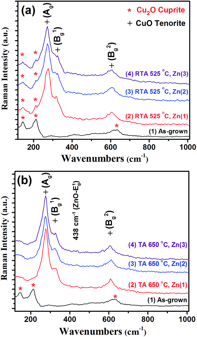 | ||
| Fig. 3 Series of micro-Raman spectra scanned of copper oxide nanocrystallites doped with different concentrations (Zn(1), Zn(2), Zn(3)) of zinc presenting the phonon modes in the top of the nanostructures corresponding to the Ag, B1g and B2g symmetries, respectively. Typical micro-Raman spectra of the: (a) CuO/Cu2O nanocrystallites RTA-annealed at 525 °C for 60 s; (b) CuO nanocrystallites TA-annealed at 650 °C for 30 min. | ||
Fig. 3 confirms continuous red-shift and the broadening of the Ag phonon mode when the Zn concentration was increased. Based on reports,69,71,72 the phonon modes in CuO single crystal shift to a lower frequency mode and the linewidth is found to broadened as a result of the nanodimensions effect.73
Coexistence of mixed phases, namely cuprite Cu2O:Zn and tenorite CuO:Zn were observed in our samples. It is considered that the peak shifts as the nanoparticle diameter changes,70 also the size effects of phonon–electron coupling74 and the polarization dependence of Raman phonon modes play an important role in the Raman shifts and lead to unconventional properties.70 Comparing the Raman spectra of CuO powder68 and single crystal,71 we note the micro-Raman peak at 288 cm−1 as Ag and 330 and 621 cm−1 as Bg modes. These wavenumbers are slightly different in comparison with those in the scientific literature (298, 345 and 632 cm−1) due to size effects.69 However, in sample c3 when the grain size is larger, micro-Raman peaks have been observed at 296, 342, and 628 cm−1, which corresponds to bulk CuO. No Cu2O modes are present in the samples after TA650-treatment, demonstrating single phase characteristics of our CuO nanomaterials. The bands at about 301, 347 and 633 cm−1, may be assigned to the Ag (296 cm−1), Bg(1) (346 cm−1) and Bg(2) (631 cm−1) modes and are in agreement with previous data.71,75 The absence of Cu2O modes76 in the micro-Raman studies of the specimens confirms the phase purity of the nanocrystals after annealing at 650 °C (TA650).
Secondary ion mass spectroscopy (SIMS) shows (see Fig. S6†) that while the concentrations of Cu and O remain constant as a function of depth, the Zn concentration varies rapidly as a function of depth and its behaviour seems to track that of the Si substrate. It is possible that the SIMS signal of Zn maybe contaminated by the Si signal.
Gas sensing response
For gas sensing investigations the fabricated gas sensor structures are mounted in a test chamber at the required operating temperature for 30 min before exposing to the designated gases in order to stabilize the electrical baseline. Reported data in literature demonstrates good selectivity and gas response of the copper oxide based sensors to ethanol vapours.14,20 Thus, we select hydrogen gas (100 ppm) and ethanol vapour (100 ppm) as our test gases to demonstrate changes in selectivity of the Zn-doped copper oxide based nano-crystalline films. The gas response is presented as S = ΔR/Rair × 100%, assuming ΔR = Rgas − Rair, Rgas and Rair are the resistances of the sensor specimen under gas exposure and in ambient air, respectively.In this work, gas sensing properties are investigated mainly in dependence of Zn concentration in copper oxide nano-crystallite films (1 μm thick). In order to determine the influences of Zn dopant content on gas sensing performances of copper oxide films, three concentrations are studied as presented above. More detailed investigations on the effect of treatment type and thickness of nano-crystalline films, as well as detailed gas sensing mechanism are reported partly in paper,81 as well as will be reported in future work.
Fig. 4a shows the gas response of the copper oxide samples with 2.8–3.0 wt% Zn to H2 gas and C2H5OH versus type of thermal annealing: as-grown Cu2O samples, TA450 and TA650-treated with 2.8 wt% Zn at operating temperature (OPT) of 400 °C, and RTA525 and RTA725-annealed with 3.0 wt% Zn at OPT of 300 °C. As-grown Zn-doped copper oxide samples demonstrated poor gas response and selectivity to hydrogen gas, SH2 ∼ 42% and SEtOH ∼ 23%, while thermal annealing improved the gas sensing characteristics of the fabricated sensor specimens. The highest gas response of the RTA sample set annealed at 525 °C with SH2 ∼ 756% and SEtOH ∼ 79% was found, having a good selectivity to hydrogen gas versus ethanol (SH2/SEtOH ≈ 9.5). Also, we investigated thermal annealing at 650 °C (samples TA650) and rapid treatment at 525 °C (samples RTA525).
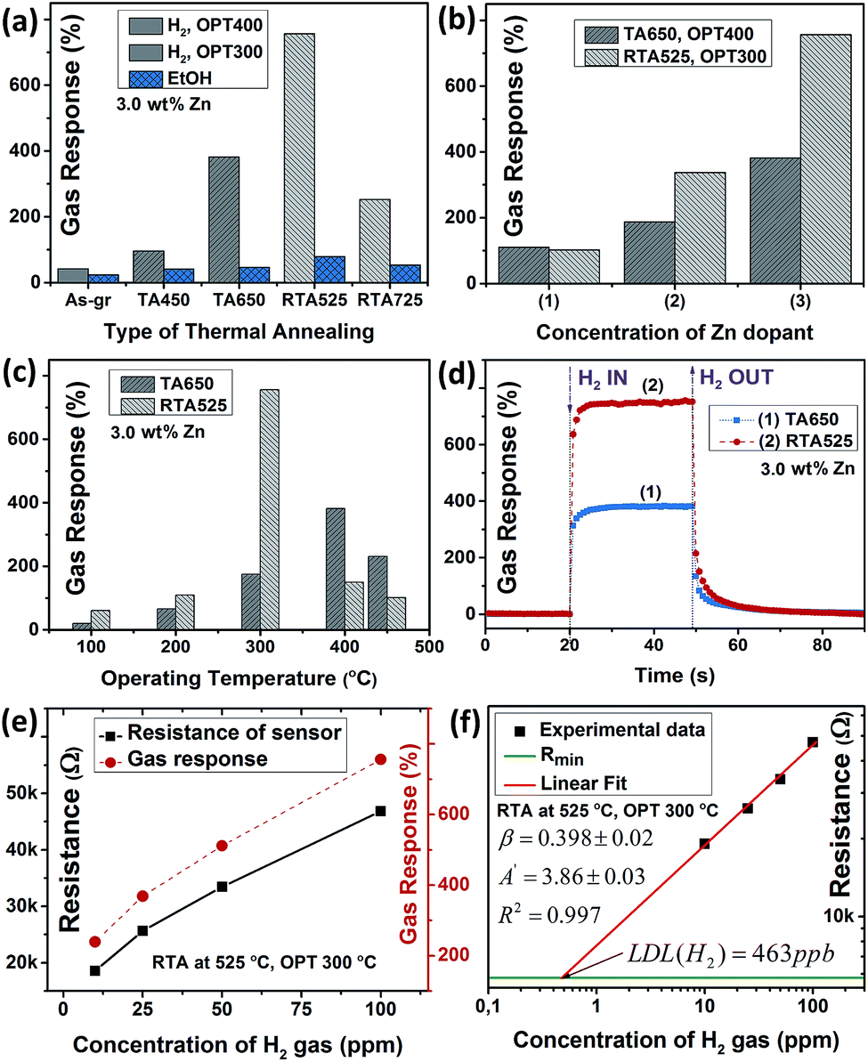 | ||
| Fig. 4 (a) Gas response of the copper oxide samples with 2.8–3.0 wt% Zn doping level versus type of thermal annealing: as-grown Cu2O samples (As-gr), TA-treated at 450 °C (TA450) and at 650 °C (TA650) at operating temperature (OPT) of 400 °C, RTA-treated at 525 °C (RTA525) and at 725 °C (RTA725) at OPT 300 °C. (b) Gas response of the sensor to H2versus content of Zn, for TA650 and RTA525. (c) Gas response to H2versus OPT of the samples with Zn(3) doping level. (d) The dynamic response of TA650 (curve 1) and RTA525 (curve 2) toward H2 at OPT of 400 °C and 300 °C, respectively. (e) Resistance and gas response of sensor toward concentrations of H2 for RTA525 at OPT 300 °C with Zn(3) doping level; (f) estimation of the lowest detection limit for H2 detection using log vs. log plot. | ||
Fig. 4b shows the response of sensor structure to hydrogen gas versus concentration of Zn dopant: Zn(1) – 1.9 wt% Zn; Zn(2) – 2.7 wt% Zn; Zn(3) – 3.0 wt% Zn in the case of RTA treated samples, as well as of Zn(1) – 1.9 wt% Zn, Zn(2) – 2.4 wt% Zn; Zn(3) – 2.8 wt% Zn in the case of TA treated samples. As expected, the gas response of the Zn-doped copper oxide based sensors increases as Zn doping concentration increases for both types of treatments, which indicates that the main factor in hydrogen gas response change is the dopant in the nanomaterial.
The optimal operating temperature (OPT) of the fabricated sensors was also investigated. Fig. 4c shows the gas response to hydrogen gas vs. OPT for the samples doped with concentration Zn(3). As observable, the OPT is higher for TA650-treated specimens when compared to the case of RTA525, 400 °C versus 300 °C, respectively. The lowest OPT is preferable for lower power consumption of the sensor heaters, thus it is a very important parameter from the industrial point of view. However, the gas response and rapidity of the sensor is strongly dependent on the OPT value.6,14,20 At low operating temperatures of below 200 °C, the hydrogen gas molecules do not possess sufficient thermal energy to react with the adsorbed oxygen molecules (e.g. O2−) on the surface of copper oxide, which lead to low reaction rate and lower gas response.77 At OPT higher than 300 °C the oxygen atoms mainly adsorb at the surface of copper oxide nano-crystallites.14,20,77 In this case, the thermal energy is sufficient to overcome the activation energy barrier of the reaction of the hydrogen molecules with ionosorbed oxygen species.20,77
Fig. 4d shows the dynamic response of sensor structures on copper oxide nano-crystalline films treated TA650 and RTA525 toward hydrogen gas at OPT of 400 °C and 300 °C, respectively. The calculated response τr and recovery τd times (as time to accomplish 90% of the full gas response and time to take 10% of full recovery to initial baseline value, respectively) are τr ∼ 1.9 s and τd ∼ 8.5 s for TA650-treated sample at OPT of 400 °C, while for the RTA525 treated one at lower OPT value was τr ∼ 2.4 s and τd ∼ 6.9 s, respectively. However, at the same OPT the RTA treated samples are faster, for example at 400 °C the τr ∼ 1.4 s and τd ∼ 5.4 s. All data on rapidity of the sensors are included in Table S1.† The best thermal annealing regime to obtain higher gas response and faster response/recovery from CuO:Zn films is RTA at 525 °C for 60 s.
Fig. 4e shows the results on sensor resistance and gas response versus concentration of hydrogen gas (pH2) of the sample treated RTA525 and measured at OPT of 300 °C with Zn(3) doping level and it is observed that the response follows a power law relationship on gas concentration SH2 ∝ pH2β, where β is the slope of logR vs. logpH2, and β = 0.398 (see Fig. 4f),14 which is in concordance with different results on copper oxide based sensors.6Fig. 4f shows the estimation of lowest detection limit (LDL) using the method reported by Volanti et al.6Rmin is defined as Rmin = Rair + 3σ0, where Rair is the resistance in air before exposure to hydrogen gas at OPT of 300 °C, and σ0 is the standard deviation of the air response.6 For calculation of σ0, the sensor was placed in the test chamber at OPT of 300 °C for 60 min, in order to stabilize the sensor resistance, and then the next 60 min before exposing to hydrogen gas are used to calculate σ0. In this work we found that σ0 = 5.43 Ω and Rmin = 5471 Ω.
The parameters obtained by linear fitting of the log vs. log plot are presented in Fig. 4f. Estimated LDL was ∼0.5 ppm of hydrogen gas which was comparable to one of the best values for CuO hydrogen gas based sensor reported in literature.6 We note the relatively low value of Rmin (in the order of kΩ), which is important during film integration in electronic devices for gas detection applications. Usually, to increase the gas response to reducing gases in case of sensors based on n-type oxide metals, one uses acceptor doping which decreases the concentration of the electrons in the semiconductor16,78 and leads to an increase in total resistance of the sensor (to MΩ range).79 As a result, the sensing measurements in laboratory conditions are possible only with high precision test measurements tools in the majority of cases. Thus, the integration in a sensor module is a problem due to the necessity of amplifiers with very high input impedance as result of the high resistance of the sensors. Therefore the total cost of the device increases. In our case, a kΩ range of the sensor resistance value can solve those problems. Also, the fast response and recovery times associated with high gas response and selectivity to hydrogen gas, demonstrated good potential for fabrication of stable, robust, low-cost and fast hydrogen gas sensor applications.
According to literature analysis, sensors based on copper oxide or other p-type metal oxide nanostructures with such high response and selectivity to hydrogen have not been reported until now by other research groups. In most cases, p-type semiconductor based sensors demonstrated good gas response to ethanol vapour and other VOCs, such as benzene acetone and toluene.16 For comparison, in Table S2† the most relevant data on the hydrogen gas sensors based on p-type and n-type oxide metal nanostructures which indicate response to hydrogen gas and ethanol vapour ratio have been presented in detail.
The effect of humidity on the gas sensitivity
To check the influence of the humidity on gas sensing performances of the copper oxide based nanostructured films, gas sensing measurements were performed in 90% RH and compared with those in 30% RH for samples treated RTA at 525 °C and TA at 650 °C with 3.0 wt% Zn (Fig. 5a and b). As can be observed, the gas response decreased in humid atmosphere by ≈35% and ≈65% for RTA and TA treated samples, respectively. Also a decrease in rapidity of the sensors can be observed (see Table S1†). Thus, the improved stability to humidity of the RTA treated samples is indicated. One of the main possible reasons could be a lower response to water vapour of the RTA treated samples (see Fig. S7†), while the decrease in gas response can be attributed to competition of adsorbed oxygen species on the surface of the CuO nanocrystals between water vapour and H2 molecules.80 More details on the influence of humidity on gas sensing performances of the Zn-doped copper oxide nanostructured films versus concentration of Zn and related mechanism have been presented in previous work.81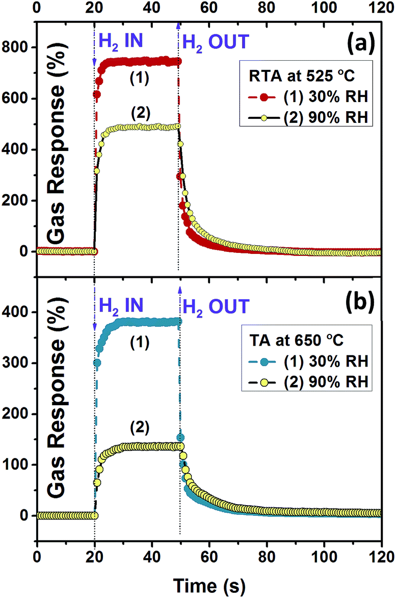 | ||
| Fig. 5 Dynamic hydrogen gas response of the samples treated RTA at 525 °C (operating temperature 300 °C) and TA-annealed at 650 °C (operating temperature 400 °C) in 30% and 90% RH. | ||
Gas sensing mechanism proposed
The reactivity of active sites on the surface of Zn-doped copper oxide nano-crystalline films is strongly dependent on its doping concentration, type of defects and impurities.78 Thus, surface phenomena are important to understand the sensing mechanism of the sensor based on p-type semiconductor nanomaterials. As we mentioned above, adsorbed oxygen can be ionized into several forms, namely atomic O− or O2− and molecular O2−.82 At temperatures below 200 °C, predominant surface oxygen species are in molecular form O2−:83| O2(g) → O2(ad) | (9) |
| O2(ad) → O2(ad)− + h(lattice)+ | (10) |
While at temperatures above 200 °C predominant surface oxygen species are atomic species O− and O2−:21
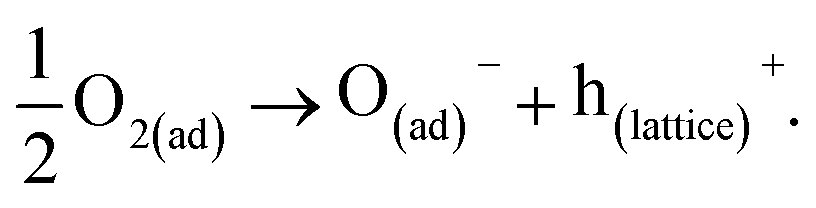 | (11) |
Ionosorbed oxygen creates the surface acceptor states and traps electrons from the valence band, which results in increased concentration of holes and resistance decreases (for p-type semiconductors).80 A schematic illustration of the proposed gas sensing mechanism is presented in Fig. 6a and b, where the transparent blue zone shows HAL with lower resistance in comparison with core region (represented by dark yellow region). At exposure to hydrogen gas the following reaction occurs (taking in account that h+ + e− = null):14
| H2(g) + O(ads)− + h+ → H2O(g) + null | (12) |
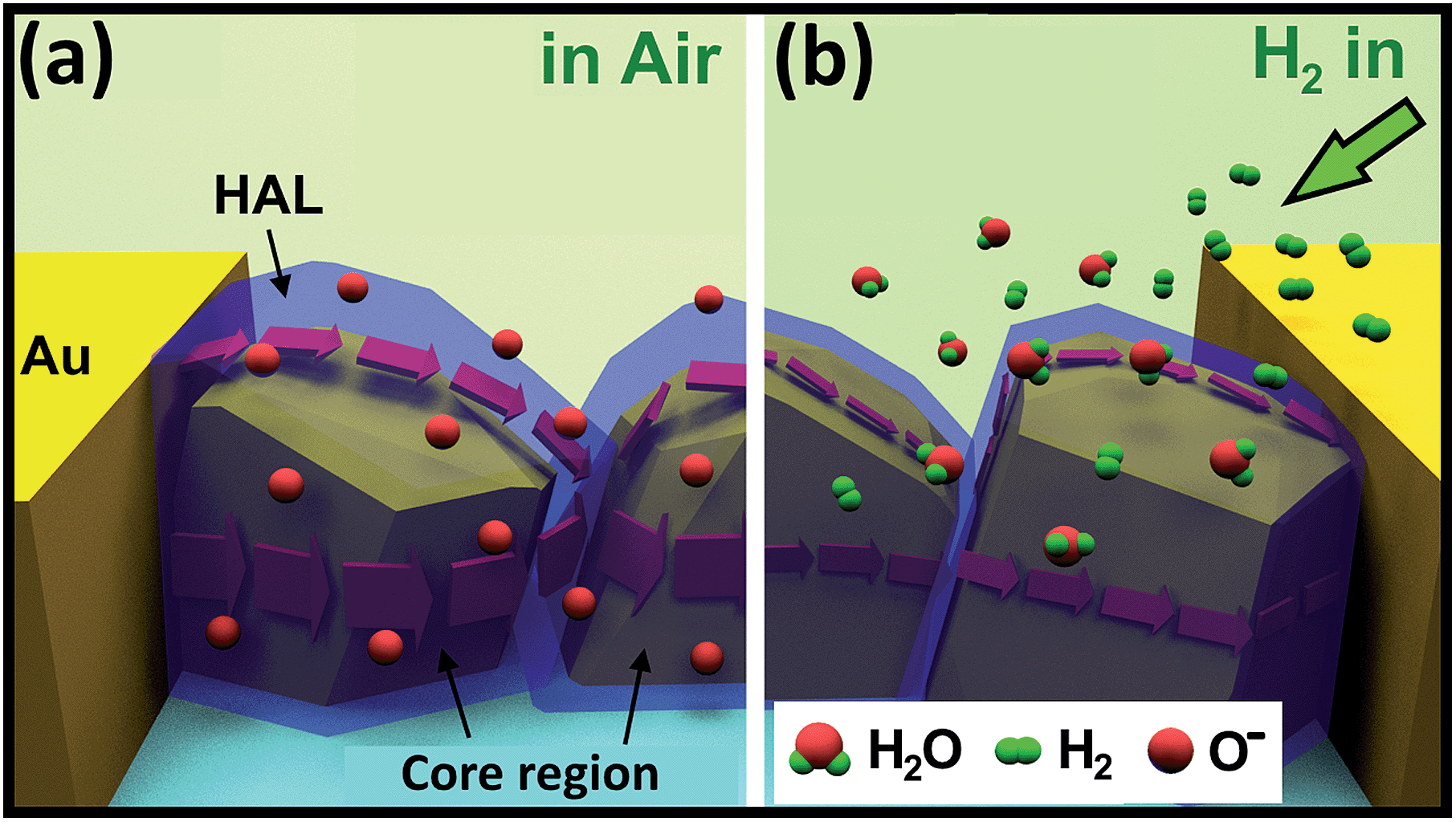 | ||
| Fig. 6 Schematic representation of H2 gas sensing mechanism for gas sensor based on Zn-doped copper oxide nano-crystalline films. (a) At exposure to ambient air, the oxygen atoms (illustrated by red spheres) are adsorbed at the surface of nano-crystallites. By trapping free electrons from the bulk, the hole accumulation layer region (HAL) with lower resistance is created, that lead to a current flow (illustrated by dark red arrows). HAL is illustrated by the blue transparent region, while core region is illustrated by dark yellow. (b) At exposure to hydrogen gas, the width of HAL region will decrease due to injected electrons from hydrogen gas molecules, which are oxidized to H2O molecules. As a result, the current flow through the HAL region will decrease, that is illustrated by smaller dark red arrows. | ||
Equation (12) is represented schematically in Fig. 6b. With decrease in the holes concentration, HAL width becomes thinner and the resistance of the sensor structure increases respectively.
Electron sensitization is known to be an efficient tool to control/tune the gas response and selectivity of the oxide metals with both types of electrical conductivity.78 In our case it is performed by control of Zn concentration in copper oxide nano-crystalline films. It has been shown that addition of zinc in copper oxide films decreases the electrical resistivity of the sensing material.13,81 For example, in the case of RTA at 525 °C the electrical resistivity of the sample was decreased from 3.1 × 10⁴ Ω cm to 1.95 × 10⁴ Ω cm by increasing Zn concentration from (#1) to (#3). The created acceptor centres are ionized at room temperature by capturing electrons from the valence band and generating holes. In general, it is assumed that Zn-doping of Cu2O results in donor doping.84
Thus, further investigations are needed to determine the acceptor centres origin related to zinc ion doping of the Cu2O and CuO. Due to different oxidation states of copper ions in Cu2O (Cu1+) and CuO (Cu2+), incorporation of Zn2+ should occur by different mechanisms. In both cases, the concentration of holes is increased, which leads to a decrease of the electrical resistance value.13,81 Taking into account that the value of the sensor resistance under exposure to gas Rgas can be theoretically very large, as a result sensor sensitivity (S = Rgas/Rair) can be improved by decreasing the Rair value.85 However, this can't explain the high selectivity to hydrogen gas of the Zn-doped copper oxide based sensors.
Since peaks of ZnO or Zn were not observed in the XRD data, it is reasonable to assume that most of Zn dopant is dispersed well on the surface of CuO nano-crystallites as amorphous ZnO,86 which was demonstrated by XPS measurements in previous work.81 Addition of ZnO to metal oxides is known to enhance the surface oxidation by H2 gas molecules, which lead to a higher selectivity to hydrogen gas.87 Yu et al.87 demonstrated an increase in hydrogen gas selectivity by addition of ZnO to pellet-type SnO2 sensors. Also, the lower response of copper oxide based sensors more likely is induced by an inhibition of ethanol vapour molecules catalytic oxidation due to Zn doping of nano-material.13,16,20,86
DFT calculations
In order to gain further insights into the H2 sensing mechanism, we performed density functional theory based calculations on the interaction of H2 with Zn-doped CuO(111) and Cu2O(111) surfaces.Next, we modelled the interaction of the H2 molecule with this Zn-doped CuO(111) surface. In a series of calculations, we first placed the H2 molecule close to all surface atoms in different orientations, but we found that the molecule desorbs from the surface in all the initial input configurations, except when it was placed near the most exposed OSUF atoms. We observed that the bonds between the surface oxygen OSUF and the CuCUS surface atoms are broken, with OSUF connecting to the H2 molecule to form an adsorbed water molecule, as shown in Fig. 7. The same OSUF is bonded to the Zn atom on the surface with a bond length of 2.022 Å. Moreover, among all the surface OSUF atoms, the most stable configuration was found by placing the H2 molecule near the OSUF atom, which is bonded to the Zn dopant atom. Our results are similar to recent work on H2 adsorption on an undoped CuO(111) surface,88 where the bond between the surface oxygen OSUF to the CuCSA atoms is broken and OSUF connects to a nearby CuCUS surface copper atom after forming a H2O molecule. Our calculated binding energy is −80.1 kJ mol−1, which is ∼8 kJ mol−1 larger than that achieved on the CuO(111) surface without Zn-doping. The charge density difference, together with Bader charge analysis (Fig. 7), shows that there is significant charge transfer between the newly formed H2O molecule and surface atoms CuCSA and OSUF. As a result of the H2 molecule interaction with the surface, the Fermi energy increases by 0.210 eV, from −1.563 to −1.353 eV, while the calculated band-gap decreases by only ∼1.3% to 0.877 eV. The calculated densities of states are shown in Fig. S10a.†
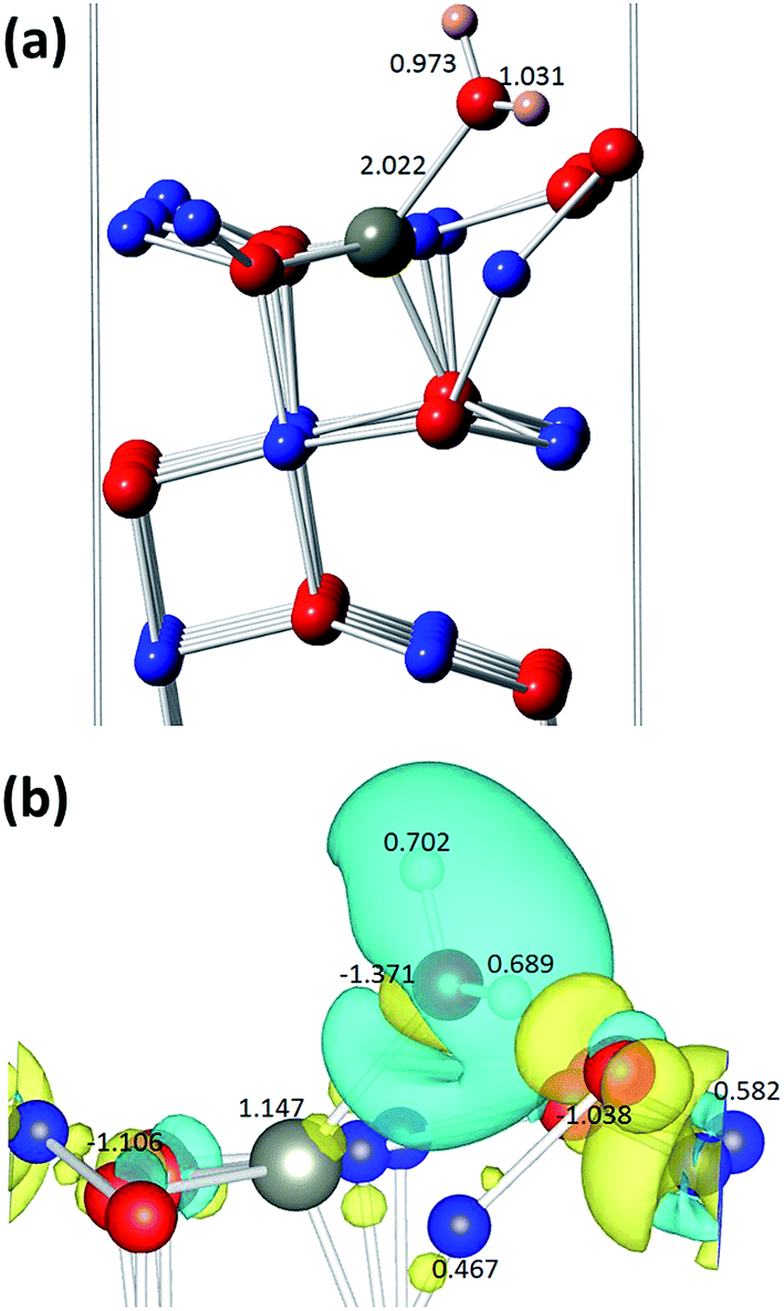 | ||
| Fig. 7 (a) Side view of H2 on the Zn-doped (2 × 1) slab of the CuO(111) surface, (b) electronic density difference plot of the H2 bonded structures on the Zn-doped CuO(111) surface, showing charge transfer in the regions between the H2 and the surface atoms upon interaction. Blue contours indicate electron density increases by 0.01 electrons Å−3 and yellow contours indicate electron density decreases by 0.005 electrons Å−3. Bader charge values are in e−. Cu, O, Zn and H atoms are represented by blue, red, grey and salmon pink colours respectively. | ||
We next investigated the interaction of the H2 molecule with the surface and found that the H2 molecule dissociates on the surface with a small binding energy of −24.6 kJ mol−1. This binding is weaker compared to that on the pristine Cu2O(111) surface without Zn-doping,42 where the calculated binding energy for the dissociative adsorption of the H2 molecule was found to be −78.6 kJ mol−1. As shown in Fig. 8, one of the H atom binds to the Zn atom with a bond length of 1.533 Å, while the other H atom binds to the nearby surface OSUF atom with a short 0.978 Å bond length. Bader charge analysis shows that one of the H atoms, bonded to Zn, accepts a charge of −0.309 e−, while the second H atom, bonded to OSUF, transfers charge to the surface OSUF atom, becoming H+ with a calculated positive charge of 0.647. As such, the hydrogen molecule has dissociated into a proton and hydride species, where one hydrogen atom transfers charge to a comparatively more electronegative surface oxygen atom, while the other hydrogen atom gains charge from a comparatively less electronegative surface Zn atom (Fig. 8). The Fermi energy of the system increases by 0.350 eV, from −1.274 to −1.239 eV, while the calculated band gap decreases slightly by ∼5% as a result of the interaction of the H2 molecule with the surface, increasing to 0.865 eV (Fig. S10†).
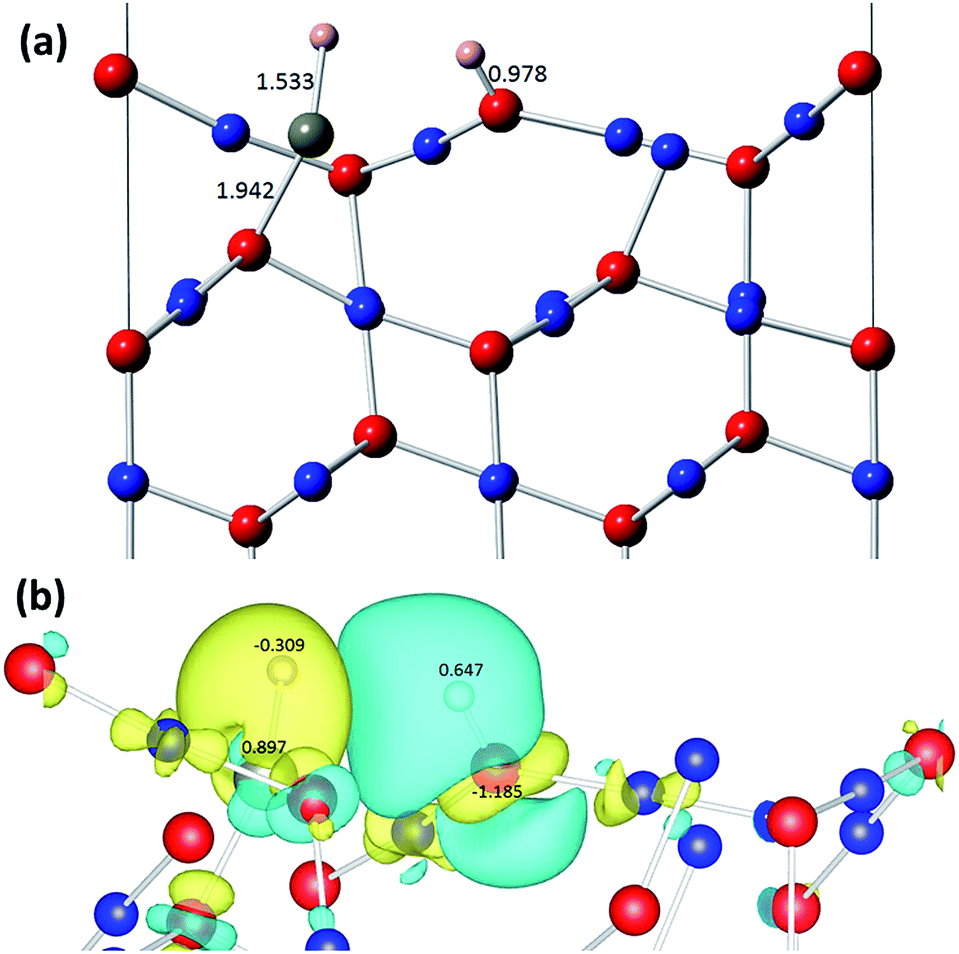 | ||
| Fig. 8 (a) Side view of H2 on the Zn-doped (2 × 1) slab of the Cu2O(111)–Cuvac surface, (b) electronic density difference plot of the H2 bonded structures on the Zn-doped Cu2O(111)–Cuvac surface, showing charge transfer in the regions between the H atoms and the surface atoms upon interaction. Blue contours indicate electron density increases by 0.01 electrons Å−3 and yellow contours indicate electron density decreases by 0.003 electrons Å−3. Bader charge values are in e−. | ||
Our calculations reveal that the Zn doping influences the binding energies of the H2 molecule on both CuO and Cu2O surfaces and charge re-distribution takes place. While the Fermi energy changes as a result of the interaction of the H2 molecule with the surface, the changes in the band-gaps are only small. Our results are similar to H2 sensing on ZnO surfaces, where the H2 molecule acts as a charge acceptor, decreasing the Fermi level by only a small change of 0.01 eV in the band gap value.89
Conclusions
Structural, morphological, chemical and vibrational properties of as-grown and post-growth thermal treated copper oxide samples prepared via SCS were investigated in details. High crystallinity, mixed Zn-doped CuO/Cu2O phase and slight changes in the crystal constants of the samples have been demonstrated. XRD and micro-Raman studies of the as-grown Cu2O layers and of the RTA treated ones (RTA525 at 525 °C for 60 s) detected two coexisting phases (cubic Cu2O and the monoclinic CuO). The two phases ratio can be controlled by the Zn-doping level in SCS and by annealing regimes of TA or RTA.Gas sensing investigations showed higher gas response and selectivity to hydrogen gas of the ZnxCu1−xOy nano-crystalline films with 3.0 wt% Zn versus pure copper oxides. By Zn doping in copper oxide and formation of a nano-heterojunction after RTA at 525 °C for 60 s it was possible to change the sensing properties from ethanol vapour (pure copper oxide) to hydrogen gas (zinc-doped copper oxide with mixed phases). For samples RTA-treated at 525 °C for 60 s at operating temperature of 300 °C the gas response for 100 ppm H2 was SH2 ∼ 765%, which corresponds to an increase of sensor resistance by one order, with fast response times (τr ∼ 2.4 s) and recovery times (τd ∼ 6.9 s). Based on literature analysis, no reports on such high hydrogen gas response and selectivity of sensors based on p-type nanomaterials, have been published to-date by other groups. High crystallinity of the samples synthesized at relatively low temperatures (≤80 °C) and the existence of mixed Zn-doped CuO/Cu2O phases resulted in better sensing properties of the sensors and demonstrated good potential for fabrication of reliable, selective and fast hydrogen sensors with high gas response. A stabile sensor performances in humid air was found for CuO:Zn by exposure of samples to rapid thermal annealing process for the first time.
Dispersion-corrected DFT + U calculations were employed to investigate the hydrogen gas sensing mechanism on both the CuO and Cu2O surfaces, which revealed that Zn doping facilitates the binding of H2 where charge transfer between the molecule and the surface is responsible for the sensing behaviour.
Such nanomaterials are of great interest for other applications where a p-type oxide is requested.
Acknowledgements
Dr Lupan acknowledges the Alexander von Humboldt Foundation for the research fellowship for experienced researchers 3-3MOL/1148833 STP at the Institute for Materials Science, University of Kiel, Germany. This research was sponsored partially by the German Research Foundation (DFG) under the scheme AD 183/12-1. This research was partly supported by the STCU within the Grant 5989. Professor Trofim Viorel (T.U.M.) is acknowledged for fruitful discussions and his support in the experimental part. AKM and NHdL acknowledge the Engineering and Physical Sciences Research Council (EPSRC) “4CU” programme grant (EP/K001329/1 and EP/K035355/1). NHdl also thanks the Royal Society for an Industry Fellowship.References
- Y. Xia, Z. Yang and Y. Zhu, J. Mater. Chem. A, 2013, 1, 9365–9381 CAS.
- X. Xiao, C. Xu, J. Shao, L. Zhang, T. Qin, S. Li, H. Ge, Q. Wang and L. Chen, J. Mater. Chem. A, 2015, 3, 5517–5524 CAS.
- R. Shabu, A. Moses Ezhil Raj, C. Sanjeeviraja and C. Ravidhas, Mater. Res. Bull., 2015, 68, 1–8 CrossRef CAS.
- L. Cheng, M. Shao, D. Chen and Y. Zhang, Mater. Res. Bull., 2010, 45, 235–239 CrossRef CAS.
- O. Lupan, G. A. Emelchenko, V. V. Ursaki, G. Chai, A. N. Redkin, A. N. Gruzintsev, I. M. Tiginyanu, L. Chow, L. K. Ono, B. Roldan Cuenya, H. Heinrich and E. E. Yakimov, Mater. Res. Bull., 2010, 45, 1026–1032 CrossRef CAS.
- D. P. Volanti, A. A. Felix, M. O. Orlandi, G. Whitfield, D.-J. Yang, E. Longo, H. L. Tuller and J. A. Varela, Adv. Funct. Mater., 2013, 23, 1759–1766 CrossRef CAS.
- O. Lupan, V. Cretu, V. Postica, M. Ahmadi, B. R. Cuenya, L. Chow, I. Tiginyanu, B. Viana, T. Pauporté and R. Adelung, Sens. Actuators, B, 2016, 223, 893–903 CrossRef CAS.
- O. Lupan, G. Chai and L. Chow, Microelectron. Eng., 2008, 85, 2220–2225 CrossRef CAS.
- H. J. Kang, P. Dai, B. J. Campbell, P. J. Chupas, S. Rosenkranz, P. L. Lee, Q. Huang, S. Li, S. Komiya and Y. Ando, Nat. Mater., 2007, 6, 224–229 CrossRef CAS PubMed.
- Y. Tokura, H. Takagi and S. Uchida, Nature, 1989, 337, 345–347 CrossRef CAS.
- S. T. Shishiyanu, T. S. Shishiyanu and O. I. Lupan, Sens. Actuators, B, 2006, 113, 468–476 CrossRef CAS.
- I. M. Tiginyanu, O. Lupan, V. V. Ursaki, L. Chow and M. Enachi, in Compr. Semic. Sci. Tech., ed. P. B. F. Kamimura, Elsevier, Amsterdam, 2011, pp. 396–479, DOI:10.1016/b978-0-44-453153-7.00105-x.
- O. Lupan, V. Cretu, V. Postica, N. Ababii, O. Polonskyi, V. Kaidas, F. Schutt, Y. K. Mishra, E. Monaico, I. Tiginyanu, V. Sontea, T. Strunskus, F. Faupel and R. Adelung, Sens. Actuators, B, 2016, 224, 434–448 CrossRef CAS.
- Y.-H. Choi, D.-H. Kim, S.-H. Hong and K. S. Hong, Sens. Actuators, B, 2013, 178, 395–403 CrossRef CAS.
- N. G. Cho, I.-S. Hwang, H.-G. Kim, J.-H. Lee and I.-D. Kim, Sens. Actuators, B, 2011, 155, 366–371 CrossRef CAS.
- H.-J. Kim and J.-H. Lee, Sens. Actuators, B, 2014, 192, 607–627 CrossRef CAS.
- L. Liao, Z. Zhang, B. Yan, Z. Zheng, Q. Bao, T. Wu, C. M. Li, Z. Shen, J. Zhang and H. Gong, Nanotechnology, 2009, 20, 085203 CrossRef CAS PubMed.
- T. B. Coplen, J. K. Böhlke, P. De Bievre, T. Ding, N. Holden, J. Hopple, H. Krouse, A. Lamberty, H. Peiser and K. Revesz, Pure Appl. Chem., 2002, 74, 1987–2017 CrossRef CAS.
- J. Han, X. Zong, X. Zhou and C. Li, RSC Adv., 2015, 5, 10790–10794 RSC.
- A. S. Zoolfakar, M. Z. Ahmad, R. A. Rani, J. Z. Ou, S. Balendhran, S. Zhuiykov, K. Latham, W. Wlodarski and K. Kalantar-Zadeh, Sens. Actuators, B, 2013, 185, 620–627 CrossRef CAS.
- C. Yang, X. Su, F. Xiao, J. Jian and J. Wang, Sens. Actuators, B, 2011, 158, 299–303 CrossRef CAS.
- N. D. Hoa, S. Y. An, N. Q. Dung, N. Van Quy and D. Kim, Sens. Actuators, B, 2010, 146, 239–244 CrossRef.
- N. D. Hoa, N. Van Quy, H. Jung, D. Kim, H. Kim and S.-K. Hong, Sens. Actuators, B, 2010, 146, 266–272 CrossRef.
- O. Lupan, V. Postica, V. Cretu, N. Ababii, M. Hoppe, T. Pauporte, B. Viana, I. Tiginyanu and R. Adelung, Microelectron. Eng., 2016 Search PubMed , under review.
- O. Lupan, L. Chow, S. Shishiyanu, E. Monaico, T. Shishiyanu, V. Şontea, B. Roldan Cuenya, A. Naitabdi, S. Park and A. Schulte, Mater. Res. Bull., 2009, 44, 63–69 CrossRef CAS.
- O. Lupan, S. Shishiyanu, L. Chow and T. Shishiyanu, Thin Solid Films, 2008, 516, 3338–3345 CrossRef CAS.
- S. T. Shishiyanu, O. I. Lupan, E. V. Monaico, V. V. Ursaki, T. S. Shishiyanu and I. M. Tiginyanu, Thin Solid Films, 2005, 488, 15–19 CrossRef CAS.
- M. T. S. Nair, L. Guerrero, O. L. Arenas and P. K. Nair, Appl. Surf. Sci., 1999, 150, 143–151 CrossRef CAS.
- V. V. Ursaki, O. I. Lupan, L. Chow, I. M. Tiginyanu and V. V. Zalamai, Solid State Commun., 2007, 143, 437–441 CrossRef CAS.
- O. Lupan, L. Chow, T. Pauporté, L. Ono, B. R. Cuenya and G. Chai, Sens. Actuators, B, 2012, 173, 772–780 CrossRef CAS.
- O. Lupan, T. Pauporte, B. Viana, P. Aschehoug, M. Ahmadi, B. R. Cuenya, Y. Rudzevich, Y. Lin and L. Chow, Appl. Surf. Sci., 2013, 282, 782–788 CrossRef CAS.
- O. Lupan, T. Pauporté, I. Tiginyanu, V. Ursaki, V. Şontea, L. Ono, B. R. Cuenya and L. Chow, Thin Solid Films, 2011, 519, 7738–7749 CrossRef CAS.
- O. Lupan, V. Cretu, M. Deng, D. Gedamu, I. Paulowicz, S. r. Kaps, Y. K. Mishra, O. Polonskyi, C. Zamponi and L. Kienle, J. Phys. Chem. C, 2014, 118, 15068–15078 CAS.
- G. Kresse and J. Hafner, Phys. Rev. B: Condens. Matter Mater. Phys., 1993, 47, 558–561 CrossRef CAS.
- G. Kresse and J. Hafner, Phys. Rev. B: Condens. Matter Mater. Phys., 1994, 49, 14251–14269 CrossRef CAS.
- G. Kresse and J. Furthmüller, Comput. Mater. Sci., 1996, 6, 15–50 CrossRef CAS.
- G. Kresse and J. Furthmüller, Phys. Rev. B: Condens. Matter Mater. Phys., 1996, 54, 11169–11186 CrossRef CAS.
- P. E. Blöchl, Phys. Rev. B: Condens. Matter Mater. Phys., 1994, 50, 17953–17979 CrossRef.
- J. P. Perdew, K. Burke and M. Ernzerhof, Phys. Rev. Lett., 1996, 77, 3865–3868 CrossRef CAS PubMed.
- J. P. Perdew, K. Burke and M. Ernzerhof, Phys. Rev. Lett., 1997, 78, 1396 CrossRef CAS.
- S. L. Dudarev, G. A. Botton, S. Y. Savrasov, C. J. Humphreys and A. P. Sutton, Phys. Rev. B: Condens. Matter Mater. Phys., 1998, 57, 1505–1509 CrossRef CAS.
- A. K. Mishra, A. Roldan and N. H. de Leeuw, J. Phys. Chem. C, 2016, 120, 2198–2214 CAS.
- M. K. Yaakob, N. H. Hussin, M. F. M. Taib, T. I. T. Kudin, O. H. Hassan, A. M. M. Ali and M. Z. A. Yahya, Integr. Ferroelectr., 2014, 155, 15–22 CrossRef CAS.
- A. K. Mishra, A. Roldan and N. H. de Leeuw, J. CO2 Util., 2016 DOI:10.1016/j.jcou.2016.02.008.
- S. Grimme, J. Comput. Chem., 2006, 27, 1787–1799 CrossRef CAS PubMed.
- H. J. Monkhorst and J. D. Pack, Phys. Rev. B: Condens. Matter Mater. Phys., 1976, 13, 5188–5192 CrossRef.
- G. Henkelman, A. Arnaldsson and H. Jónsson, Comput. Mater. Sci., 2006, 36, 354–360 CrossRef.
- Atoms in Molecules: A Quantum Theory, ed. R. F. W. Bader, Oxford University Press, London, 1994 Search PubMed.
- D. Chauhan, V. Satsangi, S. Dass and R. Shrivastav, Bull. Mater. Sci., 2006, 29, 709 CAS.
- A. v. Richthofen, R. Domnick and R. Cremer, Fresenius' J. Anal. Chem., 1997, 358, 312–315 CrossRef.
- A. Y. Oral, E. Menşur, M. H. Aslan and E. Başaran, Mater. Chem. Phys., 2004, 83, 140–144 CrossRef CAS.
- T. H. Tran and V. T. Nguyen, Int. Scholarly Res. Not., 2014, 2014, 856592 Search PubMed.
- R. D. Shannon, Acta Crystallogr., Sect. A: Cryst. Phys., Diffr., Theor. Gen. Crystallogr., 1976, 32, 751–767 CrossRef.
- O. Lupan, T. Pauporté, B. Viana and P. Aschehoug, Electrochim. Acta, 2011, 56, 10543–10549 CrossRef CAS.
- A. Li, H. Song, W. Wan, J. Zhou and X. Chen, Electrochim. Acta, 2014, 132, 42–48 CrossRef CAS.
- P. Chand, A. Gaur, A. Kumar and U. Kumar Gaur, Appl. Surf. Sci., 2014, 307, 280–286 CrossRef CAS.
- N. Mohamed Basith, J. Judith Vijaya, L. John Kennedy and M. Bououdina, Phys. E, 2013, 53, 193–199 CrossRef.
- X-ray diffraction procedures, ed. H. P. Klug and L. E. Alexander, John Wiley & Sons, inc., New York, 1954 Search PubMed.
- G. Williamson and W. Hall, Acta Metall., 1953, 1, 22–31 CrossRef CAS.
- S. Das and T. L. Alford, J. Appl. Phys., 2013, 113, 244905 CrossRef.
- I. Singh and R. K. Bedi, Appl. Surf. Sci., 2011, 257, 7592–7599 CrossRef CAS.
- D. Prabhakaran and A. T. Boothroyd, J. Cryst. Growth, 2003, 250, 77–82 CrossRef CAS.
- R. Borzi, S. Stewart, G. Punte, R. Mercader, G. Curutchet, R. Zysler and M. Tovar, J. Appl. Phys., 2000, 87, 4870–4872 CrossRef CAS.
- T. V. Thi, A. K. Rai, J. Gim and J. Kim, Appl. Surf. Sci., 2014, 305, 617–625 CrossRef CAS.
- L. Armelao, D. Barreca, M. Bertapelle, G. Bottaro, C. Sada and E. Tondello, Thin Solid Films, 2003, 442, 48–52 CrossRef CAS.
- S. Asbrink and L. J. Norrby, Acta Crystallogr., Sect. B: Struct. Crystallogr. Cryst. Chem., 1970, 26, 8–15 CrossRef CAS.
- L. Debbichi, M. Marco de Lucas, J. Pierson and P. Kruger, J. Phys. Chem. C, 2012, 116, 10232–10237 CAS.
- J. Chrzanowski and J. Irwin, Solid State Commun., 1989, 70, 11–14 CrossRef CAS.
- J. Xu, W. Ji, Z. Shen, W. Li, S. Tang, X. Ye, D. Jia and X. Xin, J. Raman Spectrosc., 1999, 30, 413–415 CrossRef CAS.
- M. H. Chou, S. B. Liu, C. Y. Huang, S. Y. Wu and C. L. Cheng, Appl. Surf. Sci., 2008, 254, 7539–7543 CrossRef CAS.
- H. Goldstein, D.-s. Kim, Y. Y. Peter, L. Bourne, J. Chaminade and L. Nganga, Phys. Rev. B: Condens. Matter Mater. Phys., 1990, 41, 7192 CrossRef CAS.
- J. Irwin, J. Chrzanowski, T. Wei, D. Lockwood and A. Wold, Phys. C, 1990, 166, 456–464 CrossRef CAS.
- H.-L. Liu, C.-C. Chen, C.-T. Chia, C.-C. Yeh, C.-H. Chen, M.-Y. Yu, S. Keller and S. P. DenBaars, Chem. Phys. Lett., 2001, 345, 245–251 CrossRef CAS.
- H. Fan, B. Zou, Y. Liu and S. Xie, Nanotechnology, 2006, 17, 1099 CrossRef CAS PubMed.
- S. K. Maji, N. Mukherjee, A. Mondal, B. Adhikary and B. Karmakar, J. Solid State Chem., 2010, 183, 1900–1904 CrossRef CAS.
- K. Reimann and K. Syassen, Phys. Rev. B: Condens. Matter Mater. Phys., 1989, 39, 11113 CrossRef.
- J. Chang, H. Kuo, I. Leu and M. Hon, Sens. Actuators, B, 2002, 84, 258–264 CrossRef CAS.
- N. Yamazoe, Sens. Actuators, B, 1991, 5, 7–19 CrossRef CAS.
- J. Fan and R. Freer, J. Appl. Phys., 1995, 77, 4795–4800 CrossRef CAS.
- M. Hübner, C. E. Simion, A. Tomescu-Stănoiu, S. Pokhrel, N. Bârsan and U. Weimar, Sens. Actuators, B, 2011, 153, 347–353 CrossRef.
- O. Lupan, V. Cretu, V. Postica, O. Polonskyi, N. Ababii, F. Schutt, V. Kaidas, F. Faupel and R. Adelung, Sens. Actuators, B, 2016, 230, 832–843 CrossRef CAS.
- J. Ding, T. J. McAvoy, R. E. Cavicchi and S. Semancik, Sens. Actuators, B, 2001, 77, 597–613 CrossRef CAS.
- R. K. Bedi and I. Singh, ACS Appl. Mater. Interfaces, 2010, 2, 1361–1368 CAS.
- A. Martínez-Ruiz, M. G. Moreno and N. Takeuchi, Solid State Sci., 2003, 5, 291–295 CrossRef.
- C. W. Na, H.-S. Woo, I.-D. Kim and J.-H. Lee, Chem. Commun., 2011, 47, 5148–5150 RSC.
- Z. Tianshu, P. Hing, Y. Li and Z. Jiancheng, Sens. Actuators, B, 1999, 60, 208–215 CrossRef.
- J. H. Yu and G. M. Choi, Sens. Actuators, B, 2001, 75, 56–61 CrossRef CAS.
- Y. Maimaiti, M. Nolan and S. D. Elliott, Phys. Chem. Chem. Phys., 2014, 16, 3036–3046 RSC.
- Q. Yuan, Y.-P. Zhao, L. Li and T. Wang, J. Phys. Chem. C, 2009, 113, 6107–6113 CAS.
Footnote |
| † Electronic supplementary information (ESI) available. See DOI: 10.1039/c6ta01355d |
| This journal is © The Royal Society of Chemistry 2016 |