
 Open Access Article
 This Open Access Article is licensed under a
 Creative Commons Attribution 3.0 Unported Licence
Improved photoelectrochemical performance of electrodeposited metal-doped BiVO4 on Pt-nanoparticle modified FTO surfaces†
Ramona
Gutkowski
a,
Daniel
Peeters
b and
Wolfgang
Schuhmann
*a
aAnalytical Chemistry – Center for Electrochemical Science (CES), Ruhr-Universität Bochum, Universitätsstr. 150, D-44780 Bochum, Germany. E-mail: wolfgang.schuhmann@rub.de
bInorganic Chemistry II, Ruhr-Universität Bochum, Universitätsstr. 150, D-44780 Bochum, Germany
First published on 26th April 2016
Abstract
The recombination of photogenerated electron–hole pairs is one of the main limiting factors of photoelectrocatalysts absorbing in the visible part of the solar spectrum. Especially for BiVO4 the slow electron transport to the back contact facilitates charge recombination. Hence, thin layers have to be used to obtain higher photocurrents which are concomitantly only allow low absorption of the incident light. To address this limitation we have modified FTO substrates with Pt-nanoparticles before electrodepositing BiVO4. The Pt-nanoparticles decrease the overpotential for the electrodeposition of BiVO4, but more importantly they provide the basis for decreased charge recombination. Electrodeposited Mo-doped BiVO4 on Pt-nanoparticle modified FTO exhibits a substantially decreased recombination of photogenerated charge carriers during frontside illumination. Simultaneous co-doping of BiVO4 with two different metals leads to a substantial enhancement of the incident-photon-to-current efficiency (IPCE) during light driven oxygen evolution reaction. Highest IPCE (>30% at 1.2 V vs. RHE) values were obtained for Mo/Zn- and Mo/B-doped BiVO4.
Introduction
Suitable materials for solar water splitting have to fulfil a number of prerequisites. The oxygen evolution reaction (OER) is the limiting half-cell reaction due to high overpotentials necessary for the four electron-transfer reaction. N-type semiconductors with low band gaps (<3.0 eV) are required for absorbing in the visible part of the solar spectrum. Thus, due to its band gap of about 2.4 eV![[thin space (1/6-em)]](https://www.rsc.org/images/entities/char_2009.gif) 1–3 and its band position suitable for oxygen evolution4 BiVO4 is regarded as a promising material for solar water splitting.5–12 BiVO4 can be deposited onto FTO substrates e.g. by a metal–organic-decomposition method followed by spin-coating13–17 or drop-casting.18 Seabold et al. developed a simple procedure for the electrodeposition of BiVO4 from a bismuth nitrate and vanadyl sulfate precursor solution,19 while Jiang et al. used an inkjet printer3 for BiVO4 deposition. Independent of the preparation method, due to the poor electron-transfer kinetics leading to high recombination rates of photo-generated electron–hole pairs BiVO4 films are not suitable for solar-energy conversion using frontside illumination. BiVO4 provides higher photocurrents or incident-photon-to-current efficiencies (IPCE) upon backside illumination.20,21 A variety of strategies to improve the photoelectrochemical performance of BiVO4 were suggested such as among others doping with different metals. For example doping with molybdenum,22–29 tungsten30–34 or simultaneously with two different metals18 leads to an increase in electron density of the doped BiVO4 resulting in higher IPCE values. To prevent the accumulation of photogenerated holes at the semiconductor/electrolyte interface due to slow OER kinetics, co-catalysts were deposited on BiVO4.16,31,35–42 Moreover, using reduced graphene oxide, Kudo et al. were able to promote electron-transfer resulting in higher IPCE values.43
1–3 and its band position suitable for oxygen evolution4 BiVO4 is regarded as a promising material for solar water splitting.5–12 BiVO4 can be deposited onto FTO substrates e.g. by a metal–organic-decomposition method followed by spin-coating13–17 or drop-casting.18 Seabold et al. developed a simple procedure for the electrodeposition of BiVO4 from a bismuth nitrate and vanadyl sulfate precursor solution,19 while Jiang et al. used an inkjet printer3 for BiVO4 deposition. Independent of the preparation method, due to the poor electron-transfer kinetics leading to high recombination rates of photo-generated electron–hole pairs BiVO4 films are not suitable for solar-energy conversion using frontside illumination. BiVO4 provides higher photocurrents or incident-photon-to-current efficiencies (IPCE) upon backside illumination.20,21 A variety of strategies to improve the photoelectrochemical performance of BiVO4 were suggested such as among others doping with different metals. For example doping with molybdenum,22–29 tungsten30–34 or simultaneously with two different metals18 leads to an increase in electron density of the doped BiVO4 resulting in higher IPCE values. To prevent the accumulation of photogenerated holes at the semiconductor/electrolyte interface due to slow OER kinetics, co-catalysts were deposited on BiVO4.16,31,35–42 Moreover, using reduced graphene oxide, Kudo et al. were able to promote electron-transfer resulting in higher IPCE values.43
Next to the above presented strategies for enhancing the photoelectrochemical performance of suitable photoabsorber materials, the insertion of interfacial layers, nanoparticles, nanotubes and nanowires, e.g. WO3 or CNTs offers a strategy to increase the charge carrier life time upon illumination with solar energy.15,44–51 We purpose as an alternative strategy the modification of the FTO substrate with Pt-nanoparticles prior to the electrochemically induced BiVO4 deposition. The presence of these nanoparticles slightly decreases the overpotential of anodic BiVO4 formation improving the low conductivity of the FTO substrate and provide nuclei centres for film growing. However, more importantly the presence of the Pt-nanoparticles within Mo-doped BiVO4 films gave rise to higher IPCE values due to decreased recombination rate of photogenerated electron–hole pairs. Doping of BiVO4 with Mo or W was found to improve additionally the photocatalytic efficiency. By doping of BiVO4 simultaneously with two metals by means of electro-deposition on Pt-nanoparticle modified FTO substrates highest IPCE values were obtained for Mo/Zn and Mo/B doped BiVO4.
Experimental part
Fluorine-doped tin oxide (FTO) substrates (Pilkington, TEC 8A, 2.3 mm) were first cleaned with acetone under ultra-sonication for 5 min followed by a treatment in 0.1 M NaOH (99%) for 15 min at 75 °C. After rinsing with water the FTO were dried in an Ar stream. All chemicals were from Sigma Aldrich if not mentioned otherwise. All electrochemical measurements were carried out in a three-electrode setup with an Ag/AgCl/3 M KCl (210 mV vs. NHE) reference electrode and a Pt wire counter electrode. Pt-nanoparticles52,53 were electrochemically deposited from a 0.4 mM H2PtCl6 (ACS reagent, ≥37.50% Pt basis) solution by applying potential pulses using a graphite rod counter electrode. A no-effect potential of 0 V was applied for 1 s, while deposition was performed for 0.2 s at −1 V. The potential pulse sequence was repeated 50 times. For the fabrication of the BiVO4 films, the electrodeposition procedure of Seabold et al. was adapted.19 In short, 35 mM VOSO4·H2O (≥97%) were diluted in 0.54 M HNO3 and 10 mM Bi(NO3)3·5H2O (≥98%) were added. For increasing the pH value up to 5, 2 M sodium acetate tetrahydrate (VWR, 100%) was used for stabilizing the Bi(III)-ions. The pH value was adjusted to 4.7 with conc. HNO3. Electrodeposition was performed at 1.9 V vs. Ag/AgCl/3 M KCl at 70 °C using a circulation thermostat and a Pt-mesh as counter electrode. It should be mentioned that the counter electrode was separated by means of a membrane from the deposition solution to prevent precipitation of Bi(0) at the Pt counter electrode. 2 M sodium acetate solution (pH 4.7) was used as electrolyte. The deposition was taking place for 400 s and 600 s on bare FTO and FTO modified with Pt-nanoparticles. The FTO substrates were contacted with an aluminium foil which was insulated during deposition with parafilm. For doping, 5 mM of the additional precursor salt was added to the described Bi–V-solution. For doping with two different metals 5 mM of each precursor salt was found to be best for depositing homogenous layers and providing high photocurrents. Zn(NO3)2·6H2O (≥99%), Na2WO4·2H2O (≥99%), Pb(NO3)3 (Riedel-de-häen, 99%), NaMoO4 (≥99%), MnSO4 (≥99%), Fe(NO3)3·9H2O (Acros, ≥99%), H3BO3 (J.T. Baker, ≥99.9%) were used for co-doping and were added directly before the electro-chemically induced deposition. After electrodeposition a brownish film was obtained, which turned into yellow after annealing in air at 500 °C for 1 h with a heating rate of 2 °C min−1. To remove vanadium pentoxide the samples were treated with 1 M KOH for 20 min.Photocurrent spectroscopy was performed using a microprocessor controlled monochromatic system (Institut Fotonowy) with integrated shutter. A short pass filter (<400 nm) and a long pass filter (>400 nm) were utilized to remove completely the undesired part of the spectrum. A 150 W Xe-Lamp (Ushio) was used as light source. All measurements were done in pyrex glass cell. If the samples were irradiated from the front, the light passes through a quartz window. The irradiated area was 0.785 cm2. The power of the incident light was determined with a power meter (Thorlabs) and a thermopile detector and was corrected by the power loss of the quartz window.
An Autolab PGSTAT12 (Metrohm) potentiostat was used to apply an external bias potential. Light induced water splitting was performed in 0.1 M Na2SO4 (p.a.) as electrolyte at a pH value of 6. The applied potential (Eapp) was re-calculated versus the reversible hydrogen electrode (RHE) by E(RHE) = 210 (mV) + Eapp + 59 × pH. The obtained photocurrents iph were derived by subtracting the dark current from the current measured under illumination (ESI, Fig. S1†) and the IPCE was calculated taking the photon flux (Φ(λ)) for each wavelength into account (eqn (1)). e represents the elementary charge.
| IPCE = iph(λ)/eΦ(λ) | (1) |
Results and discussion
Single doping of BiVO4
Before studying the influence of the back contact-modification by means of Pt-nanoparticles on the photoelectrocatalytic performance of BiVO4 or metal-doped BiVO4 the electrochemically induced deposition of BiVO4 films had to be optimized to achieve highest possible IPCE values (Fig. 1).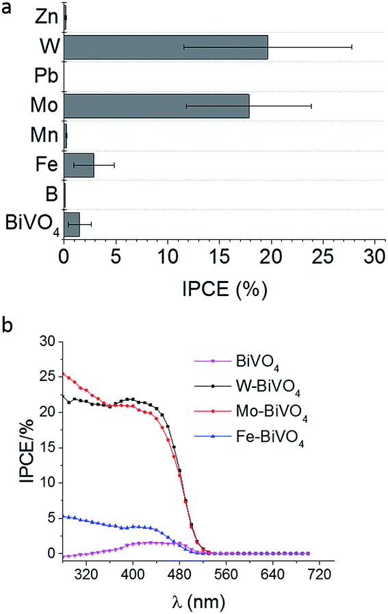 | ||
| Fig. 1 IPCE values at 450 nm and 1.2 V vs. RHE for differently doped BiVO4 films deposited on Pt-nanoparticle modified FTO (a) and IPCE spectra using frontside illumination (b). | ||
Seabold et al. achieved IPCE values of <5% at 1.2 V vs. RHE (pH 7) of undoped BiVO4 films,19 while Ding et al. reached up to 10% at 0.5 V vs. SCE (pH 9) using longer deposition times.20 These difference are attributed to the layer thickness, which is proportional to the IPCE, where very thin layers (<100 nm) results in highest IPCE values close to 40% during frontside illumination.21Fig. 1 summarizes the obtained IPCE values at 450 nm and 1.2 V vs. RHE bias potential for differently doped BiVO4 films compared with undoped BiVO4. Highest IPCE values of up to 18–20% were obtained for W- and Mo-doped BiVO4 films on Pt-nanoparticle modified FTO substrates. Doping with Fe is slightly increasing the photoelectrocatalytic efficiency, while doping with B, Mn, Zn and Pb had a negative effect leading to lower IPCE values as compared with undoped BiVO4 films. These results coincide with the screening of different metal-doped BiVO4 shown by Parmar et al.17 using the metal–organic-decomposition method and spin-coating. The IPCE spectra for the Fe, Mo, and W-doped BiVO4 films indicate a small increase of the band gap for Fe-doped BiVO4 (Fig. 1b). Concerning the band gap, direct1,18 or indirect3,48 transition is assumed for monoclinic BiVO4. The derived IPCE values demonstrate photocatalytic activity of up to 530 nm suggesting a band gap of 2.3 eV. Additionally, UV-vis absorption spectra support this finding (ESI, Fig. S3†). An indirect band gap of 2.3 eV was calculated from Tauc-plots, while a direct band gap of 2.4 eV was derived for Mo-doped BiVO4 (ESI, Fig. S1 and S2†). Recently published results from Cooper et al. suggest also an indirect band-to-band transition.54
Concept of Pt-nanoparticle modification
Regarding the electrochemically induced deposition of semi-conductor materials, the low conductivity of the used FTO substrates is leading to a high overpotential for Bi–V–O formation. Decorating the surface of the FTO with Pt-nanoparticles (50 nm diameter), small nuclei for film growth are created, thus reducing the overpotential for film formation.With increasing deposition time the Bi–V–O film is formed initially at the Pt and then in there vicinity, leading finally to a fully covered surface with a large number of small metal cores (Fig. 2b). In the simplest case, recombination of the photogenerated electron–hole pairs and in particular the absorption of the incident light depend on the layer thickness of the semiconductor material. For thick layers (d1) light absorption increases, but the recombination rate increases due to a longer diffusion length of electrons. This has a tremendous impact on the photoelectrochemical performance. In case 1 in Fig. 2a, lower photocurrents are expected for a thick layer (d1). A decrease of the recombination rate (r2) is possible by reducing the layer thickness (d2, case 2). However, by this the absorption of the incident light is concomitantly decreased limiting the PEC performance. The introduction of small Pt-nanoparticles (Fig. 2b) decrease the recombination rate at the interfacial layer between the photoabsorber and the FTO for the same layer thickness (d1) with good absorption of the incident light by electron capturing. Moreover, the advantage of the deposition of the Pt-nanoparticles e.g. over a backside metal film is seen in the ability of utilizing transparent films for tandem cell applications with an improved homogeneity of the deposited semiconductor layer on the metal nuclei. For creating uniform Pt-nanoparticles with a small diameter on the FTO surfaces sequences of potential pulses were used as reported previously.52,53 The density of the nanoparticle distribution was controlled by the number of repetitions of these pulses. Optimal conditions for uniformly sized and high density distributed Pt-nanoparticles were obtained by repeating the deposition pulses 50 times (ESI, Fig. S3†). Higher repetition numbers lead to Pt nanoparticles with increased diameter and lower density. Finally agglomeration was noticed at a 110 pulse sequence. The correlation of pulse sequences and loading of the Pt-nanoparticle is demonstrated in Fig. S4.† It is expected that the deposition of the Pt nanoparticles on FTO exhibit a substantial impact on the hydrogen evolution reaction (HER).55 An increase of the HER current was observed until a number of 110 Pt nanoparticle deposition pulse sequences. No further changes of the cathodic HER current were noticed between 110 until 350 deposition pulse sequences. In comparison to unmodified FTO, loading with Pt-nanoparticles increased the HER activity significantly with lower deposition pulse sequence number.
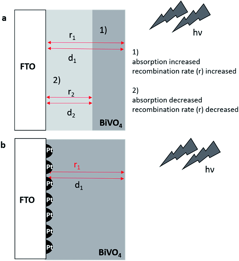 | ||
| Fig. 2 Mo-doped BiVO4 films deposited on bare FTO (a) for two different cases for thick (1) or thin (2) layers. Effect of Pt-nanoparticles on the recombination rate r and the absorption of the incident light depending on the layer thickness d (b). | ||
The influence of Pt-nanoparticles on the photocatalytic performance was studied using Mo-doped BiVO4 films because these films showed higher reproducibility as compared to W-doped BiVO4 (see Fig. 1). First, the effect of the deposited Pt-nanoparticle on the layer thickness was evaluated. Although electrode-position leads to comparatively rough surfaces, SEM cross-section allowed to estimate the layer thickness (Fig. 3).
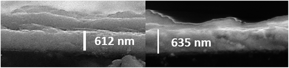 | ||
| Fig. 3 SEM cross-sections of Mo-doped BiVO4 films deposited in absence of Pt-nanoparticles (left) and in presence of Pt-nanoparticles on FTO (right). | ||
Mo-doped BiVO4 films were prepared in absence and presence of Pt-cores on the FTO surface and a similar layer thickness of around 600 ± 50 nm was obtained in both cases. Reducing the deposition time to 400 s, the layer thickness decreased around 450 ± 50 nm (ESI, Fig. S5†). These results indicate on the one side, that the layer thickness is increasing with the deposition time. On the other side, for small Pt-nanoparticles (50 nm) no influence on the film electrodeposition was observed resulting in comparable film thicknesses for layers deposited in presence and in absence of Pt-nanoparticles. Comparable layer thicknesses in accordance with the model in Fig. 2 is necessary to evaluate the effect of the Pt-nanoparticles on the recombination process during PEC measurements. Frontside illumination was used to demonstrate the impact of the Pt-cores on the photocatalytic properties of the Mo-doped BiVO4 films. It was anticipated that in presence of Pt-nanoparticles the electron transfer is facilitated leading to a substantially decreased charge-carrier recombination. Mo-doped BiVO4 films were deposited in absence and in presence of Pt-nanoparticles on FTO surfaces for 400 s and 600 s and the IPCE values were determined (Fig. 4a). At a wavelength of 450 nm an increase in the IPCE was observed when the FTO was modified with Pt-nanoparticles. This suggests a higher PEC performance due to an improved absorption of the incident light at thicker films (600 nm ± 50 nm) and an enhanced PEC performance in presence of Pt-nanoparticles.
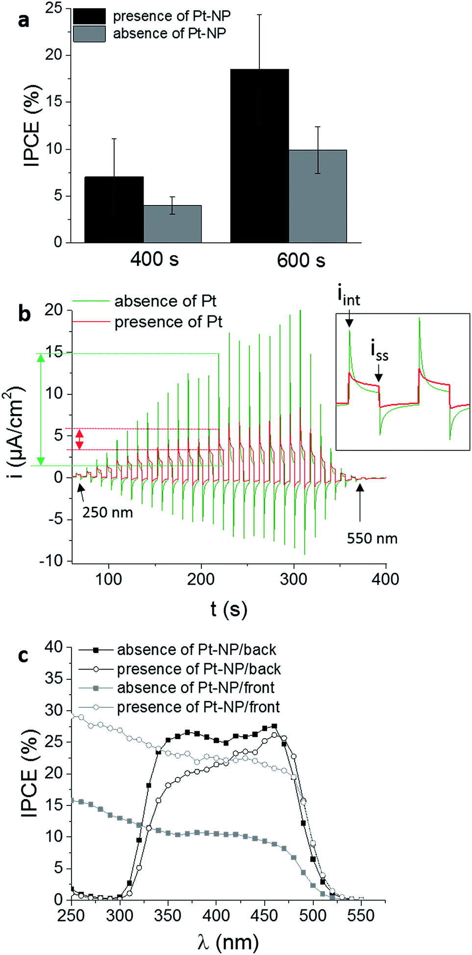 | ||
| Fig. 4 (a) IPCE values at 450 nm and a bias potential of 1.2 V vs. RHE in 0.1 M Na2SO4 for Mo-doped BiVO4 films deposited for 400 s or 600 s on bare or Pt-nanoparticles modified FTO surfaces. (b) Current–time response at a bias potential of 0.5 V vs. RHE for a Mo-doped BiVO4 films obtained with a deposition time of 600 s. During opening and closing the lamp shutter the wavelength of the incident light was increased from 250 to 550 nm. Insert: representation of the initial current (iint) and the steady-state current (iss). (c) Wavelength-dependent IPCE values with and without Pt-cores inside the Mo-doped BiVO4 film for illumination from the front and back. | ||
In a chronoamperometric experiment at a defined bias potential of 0.5 V vs. RHE the shutter of the lamp was opened and closed for predefined times. During the dark current measurement the wavelength was changed in a range from 250 nm to 550 nm (Fig. 4b). This current–time response hence does not only provide information about the wavelength-dependent photocurrent which is the basis for the determination of wave-length-dependent IPCE values, but it provides information about the recombination rate of the photogenerated electron–hole pairs. The initial current peak (iinit) measured directly when the lamp shutter was opened represents the separation of electrons and holes in the depletion region. The decay of the current results from holes, which recombine with electrons from the CB or accumulate at the surface instead of reacting with electrons from the electrolyte.56–59 The time dependent decay of the current under continuous illumination until a steady-state current (iss) is established, based on the recombination of holes in the VB with electrons from the CB, produced when the light reached for the first time the surface. This current is based on holes which did not recombine and contribute to the faradaic process.56,60 The steady state current is influenced by the recombination process at the interfacial layer and is decreased if recombination centres at the substrate are present. Moreover, this current depends on the kinetics of the reaction at the semi-conductor/electrolyte interface. Slow kinetics increases surface recombination and decreases the photocurrent. The lower the difference between iinit and iss the lower is the overall recombination rate. As a matter of fact this difference is influenced by the applied bias potential i.e. with increasing bias potential iinit decreases and iss increases (ESI, Fig. S6†).57 In order to analyse the effect of Pt-nanoparticles on the charge recombination rate a bias potential close to the open circuit potential (0.5 V vs. RHE) was applied (Fig. 4b). Consequently, the charge carrier life time is enhanced, if the ratio of the steady state current and initial current under illumination is close to one. Under comparable conditions, the ratio under illumination at 350 nm is relatively low (0.12) for Mo-BiVO4 deposited in absence of Pt-nanoparticles on FTO. The ratio increased up to four times (0.46) by in the insertion of Pt-nanoparticles between the Mo-BiVO4 layer and the FTO surface, indicating a decreased recombination of photogenerated charge carriers thus leading concomitantly to the observed higher photocurrents.
Moreover, the same samples were investigated using backside illumination through the FTO substrate (Fig. 4c). For Mo-doped BiVO4 films an improvement of the electron transport is expected due to the increased electron density caused by doping with Mo. Thus, higher photocurrents are anticipated during frontside illumination as compared with backside illumination.21,28,56 For electrodeposited Mo-doped BiVO4 on a bare FTO substrate with a thickness of the film of around 600 nm, higher IPCE values are observed for backside illumination despite the insertion of Mo into the lattice.
The IPCE values increased from around 10% to nearly 25% in the wavelength range between 350 nm and 450 nm. In this case the electron transfer to the back contact seems to be limiting. Seabold et al. observed similar effects. Thick films of several hundred nm provide higher photocurrents under backside illumination attributed to the small diffusion length of electrons of around 300 nm.22 Thin layers (<300 nm) usually exhibit higher photocurrents under frontside illumination. For Mo-doped BiVO4 films deposited on FTO modified with Pt-nanoparticles with a thickness of around 600 nm the differences between frontside and backside illumination decreased (see for details Fig. S7, ESI†). Accordingly, introduction of Pt-nanoparticles at the back contact improves electron transfer and suppresses recombination of photogenerated electron–hole pairs expecting same kinetic rates for the OER in both cases. This supports additionally the hypothesis of improved electron transfer via the Pt-nanoparticles.
Assuming direct contact between FTO and Mo-doped BiVO4 (Fig. 5a) the electrons have to diffuse through the semiconductor to the back contact, which is supposed to be limiting during frontside illumination due to the high recombination rates for photogenerated electron–hole pairs. Backside illumination reduces the diffusion length for electrons to the back contact, hence decreasing the recombination rate and terminally leading to higher photocurrents. A possible explanation of this effect is the passivation of the recombination centres of the FTO substrate, reducing the recombination of charge carriers at the interfacial layer.48 Moreover, by modifying FTO with Pt-nanoparticles a Schottky barrier between platinum and the Mo-doped BiVO4 film is generated due to the higher work function of platinum.61 Under illumination and by applying an external bias potential the photogenerated electrons can pass the energy barrier between the Pt/semiconductor contact (Fig. 5b) and are no longer available for recombination. This could explain the observed higher IPCE values as compared to Mo-doped BiVO4 films deposited in absence of Pt-nanoparticles (Fig. 4). The energy of the electrons seems to be high enough to reach the metal despite the energy barrier, while the electrons are not diffusing back to the semiconductor due to the energy barrier and the induced electric field caused by applying the external bias.
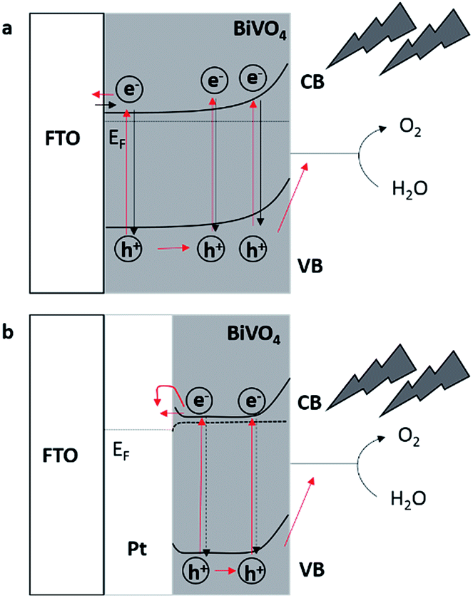 | ||
| Fig. 5 Schematic representation of recombination processes and diffusion path-ways of photogenerated electron–hole pairs in Mo-doped BiVO4 films deposited (a) on FTO and (b) on FTO modified with Pt-nanoparticles with the same layer thickness. | ||
Co-doping of BiVO4
The concept of modifying FTO substrates with Pt-nanoparticles was additionally used to further improve the photoelectrochemical performance of doped BiVO4 films by co-doping with two different metals during film electrodeposition. In contradiction to the results obtained by Park et al.,18 who obtained a moderate enhancement to maximum IPCE values of 12% with drop-casted W/Mo-doped BiVO4 films, co-doping was performed by adding a second element (Pb, Zn, B) to Mo, because the electro-deposition of Mo-BiVO4 on top of Pt-nanoparticles already yielded IPCE values up to 25%. First, the morphology and structure of the supposed metal-doped electrodeposited BiVO4 films were analysed. A possible difference in the photocatalytic efficiency is expected due to the changes of the morphology of the deposited film by adding an additional metal salt to the deposition bath (ESI, Fig. S4†). Undoped and W-doped BiVO4 form rough particles, while the overall size of these particles decreased by doping with W. Doping with Mo and an additional element like Zn and B, smaller, rounder and smoother particles are observed compared to undoped BiVO4 and Mo-BiVO4. Electrochemical deposition of BiVO4 in presence of a B or Zn precursor, led to flat and agglomerated particles forming a dense layer. This change of the particle morphology suggests the formation of Zn–Bi–V–O films during the electrodeposition and annealing procedure. Similar to Mo/Zn doping, the W-BiVO4 particles changed to a rounder shape in presence of a Zn precursor during the deposition. The effect of the doping of BiVO4 films were further characterized by means of XRD and EDX analysis (ESI; Fig. S9 and S10†). XRD patterns do not show any additional reflections from impurities such as MoOx or ZnO. However, the formation of the monoclinic scheelite structure is obvious, while a shift of the characteristic peak at 28.9°, which is attributed to the incorporation of Mo6+ instead of V5+ into the monoclinic BiVO4 structure.18 Merging of the peaks at 34.5° and 35.2° as well as the peaks at 46.8° and 47.4° into a single peak suggests the deformation of the scheelite structure.62 EDX analysis showed small amounts of Zn (<1%). In the case of Mo/Zn doping, small Zn peaks demonstrate the presence of Zn in the material (ESI; Fig. S10†).Raman spectroscopy (ESI; Fig. S11†) represents a more sensitive method to evaluate the doping of the BiVO4. Similar to XRD patterns, the shift of the symmetric stretching mode of V–O of the Raman band of 833 cm−1, indicates an incorporation of an additional metal into the VO43− tetrahedron. This stretching frequency belongs to the length of the metal bond and the above-mentioned shift to lower wavenumber suggesting an increase of the bond length. Eqn (2) determines the exponential dependence of the Raman frequency (v) on the radius (r).63
| v (cm−1) = 21349 exp(−1.9176r (Å)) | (2) |
For un-doped BiVO4 the metal bond length was calculated to be 1.6916 Å. Doping with Mo increases the bond length to 1.6979 Å and the co-doping with Mo/B or Mo/Zn to 1.701 Å. From material characterization, doping simultaneously with two elements by means of the electrodeposition method was suggested.
The photoelectrochemical performance in dependence of the different dopants combinations for BiVO4 on top of Pt-nanoparticles, exhibits no improvement of the IPCE values upon co-doping with Pb as compared to pure BiVO4. All other materials improved the IPCE values (Fig. 6a and b). For BiVO4 doped with W and an additional element, only co-doping with W/Zn and W/B increased the IPCE values as compared to only W-doped BiVO4. The low reproducibility of the W deposition might be caused by the difficult co-precipitation during the V4+-oxidation. These results are in contrast to the results reported by Park et al.,18 who did not observe any improvement for drop-casted co-doped W/Zn-BiVO4 films as compared to W-doped BiVO4 films. Also Berglund et al. reported an increase of the IPCE values of up to 30% by doping BiVO4 with W/Mo.62 The differences during co-doping are probably due to the difference in the ratio of the co-dopants which are caused by the different preparation techniques, influencing the photoelectrochemical performance. We additionally combined Mo with different elements as co-dopants for BiVO4 (Fig. 6b). The effect on the IPCE values coincides with the results for W-doped BiVO4 as shown in Fig. 6a.
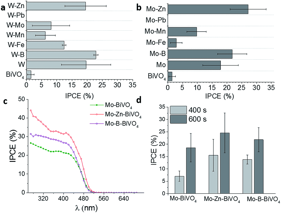 | ||
| Fig. 6 IPCE values at 450 nm for BiVO4 doped with (a) W and a second element and with (b) Mo and a second element compared to un-doped and single W- or Mo-doped BiVO4 films. Wavelength-dependent IPCE spectra for Mo-doped BiVO4 as well as Mo/Zn- and Mo/B-doped BiVO4 films (c). Influence of the electrodeposition time for different doped BiVO4 films at 450 nm. All measurements were performed in 0.1 M Na2SO4 at a bias potential of 1.2 V vs. RHE (d). | ||
The highest IPCE values were reached for Mo/Zn- and Mo/B-co-doped BiVO4 films deposited on top of Pt-nanoparticles for a deposition time of 600 s (Fig. 6d). The difference between the co-doped and the single doped Mo-BiVO4 (Fig. 6c) were significantly higher as compared to W-doped BiVO4 films. The photo-electrochemical performance of Mo-doped BiVO4 could be substantially improved and IPCE values of up to 40% were reached under frontside illumination (Fig. 6c). The exact mechanism of the co-doping is not fully understood. As already mentioned, Mo and W are well known donor-type atoms and preferentially substitute V sites. From DFT calculations performed by Yin et al.,64 Zn was suggested to act as an acceptor atom with shallow transition energy for Bi sites compared to V site substitution. Shan et al.65 reported enhanced PEC performance of BiVO4 upon B-doping attributed to the formation of weak chemical bonds between the B-ions and the corners of the VO4-tetrahedron. Additionally, higher photocatalytic activity of B-doped BiVO4 was observed by Wang et al.,66 who supposed synergetic effects of a number of factors created by B-doping, e.g. higher specific area or more oxygen vacancies. This might explain the further improvement of the IPCE in the case of Mo/B and Mo/Zn also supported by the different particle shape (see Fig. S4†).
Conclusion
A different way to improve the absorption of the incident light with increasing the layer thickness resulting in higher IPCE values was demonstrated for Mo-doped BiVO4. The associated decrease of the charge carrier life time limiting the photo-electrochemical performance was circumvented by the introduction of Pt-cores between the Mo-BiVO4 layer and the FTO surface. Two times higher IPCE values were generated in presence of Pt-nanoparticles acting as an electron scavenger preventing the electrons to recombine with the holes in the valence band. The integration of Pt-nanoparticles at the back contact of the Mo-doped BiVO4 film leads to a decrease in the recombination rate of photogenerated electron–hole pairs, which mainly represents next to the kinetic of water oxidation a limiting factor for light induced oxygen evolution at BiVO4 films. Additionally, Pt-nanoparticles favour electrochemically induced deposition of BiVO4 or doped BiVO4 films by improving the conductivity of the FTO substrate. Furthermore, the electro-deposition method can be used to simultaneously dope BiVO4 with different elements by adding an additional precursor compound to the deposition bath. Doping with Mo/Zn and Mo/B leads to a further substantial increase in the IPCE values due to an enhanced electronic conductivity.Acknowledgements
The authors are grateful to the DFG in the framework of the SPP1613 (SCHU929/12-1 and 12-2) and the Cluster of Excellence “Resolv” (EXC1069). Bastian Mei is acknowledged for performing the UV-Vis analysis.References
- S. P. Berglund, D. W. Flaherty, N. T. Hahn, A. J. Bard and C. B. Mullins, J. Phys. Chem. C, 2011, 115, 3794–3802 CAS.
- A. Kudo, K. Ueda, H. Kato and I. Mikami, Catal. Lett., 1998, 53, 229–230 CrossRef CAS.
- C. Jiang, R. Wang and B. A. Parkinson, ACS Comb. Sci., 2013, 15, 639–645 CrossRef CAS PubMed.
- A. Walsh, Y. Yan, M. N. Huda, M. M. Al-Jassim and S.-H. Wei, Chem. Mater., 2009, 21, 547–551 CrossRef CAS.
- Y. Park, K. J. McDonald and K.-S. Choi, Chem. Soc. Rev., 2013, 42, 2321–2337 RSC.
- S. Tokunaga, H. Kato and A. Kudo, Chem. Mater., 2001, 13, 4624–4628 CrossRef CAS.
- I. Vinke, J. Diepgrond, B. Boukamp, K. Vries and A. Burggaaf, Solid State Ionics, 1992, 57, 83–89 CrossRef CAS.
- A. Kudo, K. Omori and H. Kato, J. Am. Chem. Soc., 1999, 121, 11459–11467 CrossRef CAS.
- Z.-F. Huang, L. Pan, J.-J. Zou, X. Zhang and L. Wang, Nanoscale, 2014, 6, 14044–14063 RSC.
- J. Yu and A. Kudo, Adv. Funct. Mater., 2006, 16, 2163–2169 CrossRef CAS.
- A. Iwase and A. Kudo, J. Mater. Chem., 2010, 20, 7536 RSC.
- M. T. McDowell, M. F. Lichterman, J. M. Spurgeon, S. Hu, I. D. Sharp, B. S. Brunschwig and N. S. Lewis, J. Phys. Chem. C, 2014, 118, 19618–19624 CAS.
- K. Sayama, A. Nomura, T. Arai, T. Sugita, R. Abe, M. Yanagida, T. Oi, Y. Iwasaki, Y. Abe and H. Sugihara, J. Phys. Chem. B, 2006, 110, 11352–11360 CrossRef CAS PubMed.
- K. Sayama, A. Nomura, Z. Zou, R. Abe, Y. Abe and H. Arakawa, Chem. Commun., 2003, 2908 RSC.
- P. Chatchai, Y. Murakami, S.-Y. Kishioka, A. Y. Nosaka and Y. Nosaka, Electrochim. Acta, 2009, 54, 1147–1152 CrossRef CAS.
- T. H. Jeon, W. Choi and H. Park, Phys. Chem. Chem. Phys., 2011, 13, 21392–21401 RSC.
- K. P. S. Parmar, H. J. Kang, A. Bist, P. Dua, J. S. Jang and J. S. Lee, ChemSusChem, 2012, 5, 1926–1934 CrossRef CAS PubMed.
- H. S. Park, K. E. Kweon, H. Ye, E. Paek, G. S. Hwang and A. J. Bard, J. Phys. Chem. C, 2011, 115, 17870–17879 CAS.
- J. A. Seabold and K.-S. Choi, J. Am. Chem. Soc., 2012, 134, 2186–2192 CrossRef CAS PubMed.
- C. Ding, J. Shi, D. Wang, Z. Wang, N. Wang, G. Liu, F. Xiong and C. Li, Phys. Chem. Chem. Phys., 2013, 15, 4589–4595 RSC.
- F. F. Abdi and R. van de Krol, J. Phys. Chem. C, 2012, 116, 9398–9404 CAS.
- J. A. Seabold, K. Zhu and N. R. Neale, Phys. Chem. Chem. Phys., 2014, 16, 1121–1131 RSC.
- W. Luo, Z. Li, T. Yu and Z. Zou, J. Phys. Chem. C, 2012, 116, 5076–5081 CAS.
- S. K. Pilli, T. E. Furtak, L. D. Brown, T. G. Deutsch, J. A. Turner and A. M. Herring, Energy Environ. Sci., 2011, 4, 5028 CAS.
- M. Zhou, J. Bao, Y. Xu, J. Zhang, J. Xie, M. Guan, C. Wang, L. Wen, Y. Lei and Y. Xie, ACS Nano, 2014, 8, 7088–7098 CrossRef CAS PubMed.
- W. Luo, Z. Yang, Z. Li, J. Zhang, J. Liu, Z. Zhao, Z. Wang, S. Yan, T. Yu and Z. Zou, Energy Environ. Sci., 2011, 4, 4046–4051 CAS.
- W. Yao, H. Iwai and J. Ye, Dalton Trans., 2008, 1426–1430 RSC.
- L. Chen, F. M. Toma, J. K. Cooper, A. Lyon, Y. Lin, I. D. Sharp and J. W. Ager, ChemSusChem, 2015, 8, 1066–1071 CrossRef CAS PubMed.
- K. Ding, B. Chen, Z. Fang, Y. Zhang and Z. Chen, Phys. Chem. Chem. Phys., 2014, 16, 13465–13476 RSC.
- H. Ye, J. Lee, J. S. Jang and A. J. Bard, J. Phys. Chem. C, 2010, 114, 13322–13328 CAS.
- D. K. Zhong, S. Choi and D. R. Gamelin, J. Am. Chem. Soc., 2011, 133, 18370–18377 CrossRef CAS PubMed.
- S. K. Cho, H. S. Park, H. C. Lee, K. M. Nam and A. J. Bard, J. Phys. Chem. C, 2013, 117, 23048–23056 CAS.
- H. Ye, H. S. Park and A. J. Bard, J. Phys. Chem. C, 2011, 115, 12464–12470 CAS.
- H. S. Park, H. C. Lee, K. C. Leonard, G. Liu and A. J. Bard, ChemPhysChem, 2013, 14, 2277–2287 CrossRef CAS PubMed.
- M. de Respinis, K. S. Joya, H. J. M. De Groot, F. D'Souza, W. A. Smith, R. van de Krol and B. Dam, J. Phys. Chem. C, 2015, 119, 7275–7281 CAS.
- R. Li, H. Han, F. Zhang, D. Wang and C. Li, Energy Environ. Sci., 2014, 7, 1369–1376 CAS.
- S. K. Choi, W. Choi and H. Park, Phys. Chem. Chem. Phys., 2013, 15, 6499–6507 RSC.
- J. H. Kim, J. W. Jang, H. J. Kang, G. Magesh, J. Y. Kim, J. H. Kim, J. Lee and J. S. Lee, J. Catal., 2014, 317, 126–134 CrossRef CAS.
- F. Lin, D. Wang, Z. Jiang, Y. Ma, J. Li, R. Li and C. Li, Energy Environ. Sci., 2012, 5, 6400 CAS.
- M. F. Lichterman, M. R. Shaner, S. G. Handler, B. S. Brunschwig, H. B. Gray, N. S. Lewis and J. M. Spurgeon, J. Phys. Chem. Lett., 2013, 4, 4188–4191 CrossRef CAS.
- Y. Liang and J. Messinger, Phys. Chem. Chem. Phys., 2014, 16, 12014–12020 RSC.
- W. He, R. Wang, L. Zhang, J. Zhu, X. Xiang and F. Li, J. Mater. Chem. A, 2015, 3, 17977–17982 CAS.
- Y. H. Ng, A. Iwase, A. Kudo and R. Amal, J. Phys. Chem. Lett., 2010, 1, 2607–2612 CrossRef CAS.
- P. M. Rao, L. Cai, C. Liu, I. S. Cho, C. H. Lee, J. M. Weisse, P. Yang and X. Zheng, Nano Lett., 2014, 14, 1099–1105 CrossRef CAS PubMed.
- S. K. Pilli, R. Janarthanan, T. G. Deutsch, T. E. Furtak, L. D. Brown, J. A. Turner and A. M. Herring, Phys. Chem. Chem. Phys., 2013, 15, 14723–14728 RSC.
- H. W. Jeong, T. H. Jeon, J. S. Jang, W. Choi and H. Park, J. Phys. Chem. C, 2013, 117, 9104–9112 CAS.
- P. Chatchai, S.-Y. Kishioka, Y. Murakami, A. Y. Nosaka and Y. Nosaka, Electrochim. Acta, 2010, 55, 592–596 CrossRef CAS.
- Y. Liang, T. Tsubota, L. P. A. Mooij and R. van de Krol, J. Phys. Chem. C, 2011, 115, 17594–17598 CAS.
- R. Gutkowski and W. Schuhmann, Phys. Chem. Chem. Phys., 2016, 18, 10758–10763 RSC.
- A. Kongkanand, R. M. Domínguez and P. V. Kamat, Nano Lett., 2007, 7, 676–680 CrossRef CAS PubMed.
- J. Resasco, H. Zhang, N. Kornienko, N. Becknell, H. Lee, J. Guo, A. L. Briseno and P. Yang, ACS Cent. Sci., 2016, 2, 80–88 CrossRef CAS.
- X. Chen, N. Li, K. Eckhard, L. Stoica, W. Xia, J. Assmann, M. Muhler and W. Schuhmann, Electrochem. Commun., 2007, 9, 1348–1354 CrossRef CAS.
- S. Schwamborn, M. Etienne and W. Schuhmann, Electrochem. Commun., 2011, 13, 759–762 CrossRef CAS.
- J. K. Cooper, S. Gul, F. M. Toma, L. Chen, Y.-S. Liu, J. Guo, J. W. Ager, J. Yano and I. D. Sharp, J. Phys. Chem. C, 2015, 119, 2969–2974 CAS.
- E. Kemppainen, A. Bodin, B. Sebok, T. Pedersen, B. Seger, B. Mei, D. Bae, P. C. K. Vesborg, J. Halme, O. Hansen, P. D. Lund and I. Chorkendorff, Energy Environ. Sci., 2015, 8, 2991–2999 CAS.
- P. Salvador, J. Phys. Chem., 1985, 89, 3863–3869 CrossRef CAS.
- P. Salvador and C. Gutiérrez, J. Electroanal. Chem., 1984, 160, 117–130 CrossRef CAS.
- L. Peter, Chem. Rev., 1990, 90, 753–769 CrossRef CAS.
- C. Y. Cummings, F. Marken, L. Peter, A. A. Tahir and K. G. U. Wijayantha, Chem. Commun., 2012, 48, 2027–2029 RSC.
- L. Peter, K. G. U. Wijayantha and A. A. Tahir, Faraday Discuss., 2012, 155, 309–322 RSC.
- L. J. Brillson and Y. Lu, J. Appl. Phys., 2011, 109, 121301 CrossRef.
- S. P. Berglund, A. J. E. Rettie, S. Hoang and C. B. Mullins, Phys. Chem. Chem. Phys., 2012, 7065–7075 RSC.
- S. M. Thalluri, C. Martinez Suarez, M. Hussain, S. Hernandez, A. Virga, G. Saracco and N. Russo, Ind. Eng. Chem. Res., 2013, 52, 17414–17418 CrossRef CAS.
- W.-J. Yin, S.-H. Wei, M. M. Al-Jassim, J. Turner and Y. Yan, Phys. Rev. B: Condens. Matter Mater. Phys., 2011, 83 CAS.
- L. W. Shan, G. L. Wang, J. Suriyaprakash, D. Li, L. Z. Liu and L. M. Dong, J. Alloys Compd., 2015, 636, 131–137 CrossRef CAS.
- M. Wang, H. Zheng, J. Liu, D. Dong, Y. Che and C. Yang, Mater. Sci. Semicond. Process., 2015, 30, 307–313 CrossRef CAS.
Footnote |
| † Electronic supplementary information (ESI) available: Additional information contain further characterization (Raman and EDX measurements), band gap determination from wavelength dependent photocurrent spectroscopy and SEM images of the different doped BiVO4 films. Optimization of the Pt-NP deposition on FTO substrates is shown. See DOI: 10.1039/c6ta01340f |
| This journal is © The Royal Society of Chemistry 2016 |