
 Open Access Article
 This Open Access Article is licensed under a
 Creative Commons Attribution 3.0 Unported Licence
Influence of the composition of hybrid perovskites on their performance in solar cells
Josep
Albero
a,
Abdullah M.
Asiri
b and
Hermenegildo
García
*a
aInstituto Universitario de Tecnología Química CSIC-UPV, Univ. Politécnica de Valencia, Avda. De los Naranjos s/n, 46022, Spain. E-mail: hgarcia@qim.upv.es; Tel: +34 963877807
bCenter of Excellence for Advanced Materials Reseach, King Abdulaziz University, Jeddah, Saudi Arabia
First published on 10th February 2016
Abstract
During the last 5 years, power conversion efficiencies of hybrid (organic–inorganic) halide perovskite solar cells have shown impressive advances. This success has been partly due to the advances in thin film deposition techniques, but also due to the understanding of the chemical and structural characteristics of the hybrid organic–inorganic perovskites that make it possible to modulate their optoelectronic properties. Moreover, engineering the chemical composition of these materials still remains a powerful tool for further improvement of the photovoltaic activity of these materials. The preparation of efficient lead-free hybrid perovskites exhibiting reduced toxicity is one of the main targets. Besides environmental issues, the control of the composition of hybrid perovskites should be used to achieve a decrease in the bandgap energy, trying to extend the photoresponse of the materials into the NIR region. A third target is the long-term stability of devices, a property closely related to the negative influence of humidity and phase transition. This review focuses on showing how the modification of the composition of each of the three components (organic cation, metal and inorganic anion) of the parent hybrid halide perovskite (CH3NH3PbI3) influences the optoelectronic properties, photovoltaic efficiency and stability of these striking materials.
 Josep Albero | Josep Albero was born in 1980. He obtained the Chemical Engineering degree from the Jaume I University of Castellon (Spain) in 2005. Later he obtained his M.Sc. degree from Rovira I Virgili University in 2009. He worked in the synthesis and characterization of nanocrystalline semiconductor quantum dots for photovoltaic applications when he received his PhD in the group of E. Palomares at ICIQ. Afterwards he joined the H. Garcia group in ITQ as a postdoctoral fellow. His research interests are the charge transfer reactions in nanostructured materials and their applications in renewable energies. |
 Abdullah M. Asiri | Abdullah M. Asiri received his PhD from the University of Wales, College of Cardiff, UK, in 1995. He has been the Head of the Chemistry Department at King Abdulaziz University since October 2009 and he is the founder and the Director of the Center of Excellence for Advanced Materials Research. He is a Professor of Organic Photochemistry. His research interests cover color chemistry, synthesis of novel photochromic, thermochromic systems, synthesis of novel coloring matters and dyeing of textiles, Materials Chemistry, Nanochemistry and Nanotechnology Polymers and plastics. He is the Editor-in-Chief of King Abdulaziz University Journal of Science. He is also a member of the Editorial Board of Pigments and Resin Technology (UK), Organic Chemistry in Sight (New Zealand), Designed Monomers & Polymers and Journal of Single Molecule Research. He is the Vice-President of Saudi Chemical Society (Western Province Branch). He has co-authored over 500 papers and three book chapters and holds three international patents. |
 Hermenegildo García | Hermenegildo García is a full Professor at the Instituto de Tecnología química of the Technical University of Valencia, a joint center of the Technical University of Valencia and the Spanish National Research Council and a Honorary Adjunct Professor at the Center of Excellence in Advanced Materials Research of King Abdulaziz University. He made a postdoctoral stay at the University of Reading with Professor Andrew Gilbert and several sabbatical leaves in the group of Professor J. C. Scaiano at the University of Ottawa. Prof. Garcia has been active in the field of heterogeneous catalysis working with porous catalysts and nanoparticles, has published over 600 papers and has filed over 25 patents. Prof. Garcia is doctor Honoris Causa from the University of Bucharest and the recipient of the 2011 Janssen-Cilag award given by the Spanish Royal Society of Chemistry and the 2008 Alpha Gold of the Spanish society of Glass and Ceramics. |
Introduction
Organic–inorganic perovskite solar cells have erupted in the field of photovoltaics with such an impetus that according to data extracted from the Web of Science the number of publications in the last few years has grown exponentially, going from less than 20 in 2012 to more than 220 in 2014, receiving more than 5000 citations in that year, and it can be foreseen that this tendency will continue at an increasing pace in the following years. The considerable attention on hybrid (organic–inorganic) perovskite technology has arisen from the fast power conversion efficiency improvements that this material has achieved in photovoltaic devices. Since the first report in 2009 where 3.8% efficient devices were reported for CH3NH3PbI3 perovskites as an inorganic sensitizer in photoelectrochemical solar cells using an I−/I3− liquid electrolyte,1 remarkable efficiency records have been continuously attained in short intervals, this evolution contrasting favorably with conventional dye-sensitized solar cells. The substitution of liquid electrolytes by solid state hole conductors such as spiro OMeTAD (2,2′,7,7′-tetrakis-(N,N-di-4-methoxyphenylamino)-9,9′-spirobifluorene) pushed rapidly efficiencies up to 8%, overcoming the negative effect of perovskite solvation in acetonitrile. Moreover, the use of a mesoporous Al2O3 layer instead of an n-type TiO2 semiconductor increased even higher the device efficiency up to 10.9% using the mixed halide CH3NH3PbI3(Cl) in 2012.2 Continuous progress has been made since then, combining adapted film processing conditions with material design, resulting in efficient devices up to 19.3% (from a reverse-bias current–voltage curve) presented in 2014.3 More recently, researchers in the Korea Research Institute of Chemical Technology (KRICT) presented a certified perovskite solar cell of 20.1% that is probably the current efficiency record at this moment.4 Consequently, perovskite solar cells are nowadays serious competitors to the thin film technologies based on semiconductor chalcogenides such as CdTe or copper indium gallium selenide (CIGS).Intensive research has been carried out to determine the properties of the hybrid halide perovskite as a function of the composition. The general chemical formula of perovskites follows a AMX3 pattern, where A (smaller) and M (larger) represent two cations of different sizes, A being organic in the present case, and X an anion (Scheme 1). This general formula allows a large variety of compositions, including oxides, nitrides or halides, which may form different crystalline phases (cubic, tetragonal or orthorhombic) and structures (3D or 2H), including distorted structures (Scheme 2). As a consequence of this variety of compositions and structures, perovskites exhibit a wide range of physical and chemical properties such as ferro- and piezoelectricity, magnetism, superconductivity, semiconductivity and catalytic activity.
 | ||
| Scheme 1 General crystal structure of a typical hybrid perovskite. | ||
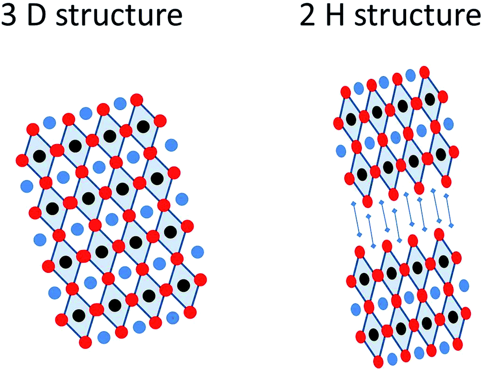 | ||
| Scheme 2 Pictorial illustration of the 3D and 2H structures of a perovskite. | ||
There have been two main reasons for these significant performance improvements in such a short period of time. On one hand, the formation of dense, high quality, continuous and crystalline thin films of organic–inorganic perovskites, through optimized processing chemistry.3,5,6 On the other hand, optimization of the composition of the material by incorporation of different organic cations (A), metal cations (M) and halide anions (X) into the perovskite composition has been a second strategy to increase solar cell efficiency.7,8 This composition optimization constitutes the focus of the present review.
Two device architectures have been extensively used in perovskite solar cells: the planar heterojunction and the mesostructured cell (Scheme 3). In the first case, a flat perovskite layer is sandwiched between selective n- and p-type semiconductors, while in the second case, perovskites are infiltrated into a mesoporous layer which can be either an n-type semiconductor material or an insulator which acts as a rigid matrix. In both cases, several methodologies have been developed to fabricate notably efficient hybrid halide perovskite solar cells.
 | ||
| Scheme 3 Illustration of the two main hybrid perovskite solar cell architectures. | ||
The easiest method for device preparation is based on the straightforward formation of most common hybrid perovskites and consists of one step deposition, in which two precursors, the metal halide and the organic halide, in a common organic solvent, are mixed together and subsequently deposited on a substrate by spin coating (Scheme 4). This method has been used both for solar cells based on planar surfaces and mesoporous layers, but is particularly suitable for perovskite deposition in mesoporous layers. Initial reports state that spin coating directly onto compact, flat substrates in planar heterojunction architectures resulted in unsatisfactory surface coverage and, therefore, in poor device performance as well as low device reproducibility due to dewetting effects.9 It has been widely reported that device performance strongly depends on the film morphology. This is a consequence, on one hand, of the inefficient charge carrier transport and diffusion length which may produce losses on the current density of the devices at short circuit.10,11 On the other hand, inappropriate film morphology promotes the presence of defects in the film and crystal grain boundaries which act as carrier traps, enhancing recombination events as well as hysteresis effects, which causes inaccuracy in the characteristic I–V measurements.12,13 Morphology control was improved through careful processing condition optimization. Inert processing environments, optimized spin coating conditions and adequate annealing temperature control allowed improvements in film morphology and, therefore, the efficiency of devices was enhanced.6 In addition, composition engineering by precursor selection [i.e. PbCl2, PbI2 or Pb(OAc2)] was found to be crucial to obtain faster and more uniform crystallization during deposition, thus, improving the device efficiencies up to 14% by using Pb(OAc)2 as the precursor.6 Despite the improved film properties that processing conditions and composition engineering have achieved in the one step deposition method, still some variations in the film thickness have been found,14 leading to low reproducibility of efficiency of these devices. In contrast, more uniform perovskite films have been achieved using dual source coevaporation of the precursors14 (Scheme 4). Solvent engineering has been also proposed as an effective method in order to improve the film morphology. In this regard, solvent mixtures of dimethylsulfoxide and γ-butyrolactone have been employed in the preparation of CH3NH3Pb(I1−xBrx)3 perovskites followed by toluene drop casting. This procedure yielded extremely uniform and dense perovskite layers due to the formation of a more stable phase that retards the fast CH3NH3I(Br) and PbI(Br)2 reaction.15 In a similar way, Park and coworkers described the formation of a 1![[thin space (1/6-em)]](https://www.rsc.org/images/entities/char_2009.gif) :1:1 adduct of CH3NH3I–PbI2–DMSO by spin coating on DMF solution and subsequent diethyl ether addition to remove the excess of less-volatile solvents.
:1:1 adduct of CH3NH3I–PbI2–DMSO by spin coating on DMF solution and subsequent diethyl ether addition to remove the excess of less-volatile solvents.
 | ||
| Scheme 4 Three general methodologies, coevaporation, one step solution method and two step solution methods, employed for the deposition of hybrid perovskites. | ||
In this way, they obtained highly efficient (∼19%) and reproducible perovskite solar cells.16
Improved particle morphology control has been achieved through a two-step deposition method (Scheme 4). In this method, the metal halide precursor is deposited either in the mesoporous layer or on the flat substrate. After an annealing treatment, the metal halide layer is exposed to the organic halide precursor by soaking the supported metal halide layer in an organic halide solution17 or by exposing the film to the precursor vapor.18
A two-step method in which the two precursor materials were sequentially spin coated one on top of the other has been also reported and the perovskite formation is achieved by reactant diffusion.19,20
The systematic morphology control of the perovskite films that can be achieved with the deposition technologies has provided comprehensive understanding of the nucleation and growth steps occurring in the perovskite formation, and this information has been very useful for device optimization. For further detailed coverage of the perovskite crystal growth methods and reported deposition techniques the reader should refer to the existing literature in this topic.5,6,8,21–23
Besides selection of the adequate film formation technique, further improvements can be achieved through design and careful control of the hybrid perovskite composition and by improvement of the synthetic procedures. In this review, we have focused on the influence on the device performance derived from the systematic substitution of organic and metal cations or halide anions in the prototypical CH3NH3PbI3 perovskite.
In spite of the efficiency enhancement due to the reduced light losses and optimized optical and electronic properties achieved through improved processing with the parent CH3NH3PbI3 perovskite, some remaining important issues that cannot be solved by film formation are still under discussion. Firstly, the search for lead-free nontoxic perovskites is one of the main objectives in order to introduce this type of photovoltaic cell in the commercial market without causing environmental concerns. A second point is to extend the spectral response of the photoactive perovskite towards the NIR part of the spectra to harvest the maximum possible sunlight. A third crucial problem to be solved is the ambient condition instability exhibited by CH3NH3PbI3 perovskite. The main instability issue arises from the moisture sensitivity that this material presents. Therefore, new strategies in the composition are desirable in order to obtain moisture stable perovskites. Moreover, it has been reported that the other instability source could arise from the phase transition from the tetragonal to the cubic structure that typically takes place at about 330 K for this material.24 Therefore, perovskite compositions having a tetragonal structure and improved stability are also highly desirable. Other properties to be improved by suitable composition optimization are the crystal size and phase, bandgap tuning, recombination control, charge transport properties and reduction of the J–V hysteresis.
Among all perovskite compositions, hybrid organic–inorganic perovskites and their derivatives have come under the spotlight in photovoltaics during the last few years due to the excellent optical and electronic properties that they have demonstrated, boosting device efficiencies up to 20% under 1 Sun illumination. The AMX3 composition is retained in these hybrid perovskites, A being an organic cation. The most employed perovskite in photovoltaic applications corresponds to a 3D structure perovskite formed by methyl ammonium as an organic cation, lead as a metal and iodine as an inorganic anion (CH3NH3PbI3). Nevertheless, several alternatives for each one of the different components (A, M and X) of these hybrid perovskites have been explored with the aim of overcoming the existing limitation in the field. In the following sections, we will describe the different composition alternatives to the archetypical CH3NH3PbI3 perovskite widely employed in photovoltaics and their impact on the photoresponse and stability of the resulting material.
The organic cation
It is well established that the organic cation in hybrid perovskites determines the perovskite structure and dimensionality, influencing some optoelectronic properties as well as the perovskite stability. The cation size can be responsible for lattice expansion or contraction, leading to bandgap modification (Scheme 5). This is a consequence of the four edge-sharing MX6 octahedra, which only allow small cations into the 3D perovskite structure. In fact, a tolerance factor has been applied in order to define the limits on ionic sizes of each component.25 Theoretical calculations have predicted that different organic cations, in addition to contributing to the structural distortion of the inorganic octahedra because of their size, affect the crystal structure due to the electrostatic interaction between the acidic hydrogens in the organic cation and the inorganic halogens, through hydrogen bonding, promoting a red-shift in the absorption onset and improving the charge transport properties of these devices.26 Nevertheless, CH3NH3+ with an ionic radius of 0.217 nm has been the most employed cation and some of the best device performances have been reported comprising always this organic cation in the hybrid perovskite composition.7 However, other organic cations with a larger or smaller radius have been also reported. The interest in replacing CH3NH3+ by different cations comes from, on one hand, the well-known undesirable moisture sensitivity of CH3NH3PbI3 and, on the other hand, from the reversible phase transition of this perovskite composition between tetragonal and cubic at 57 °C.24 This temperature usually falls within the device operating temperature, affecting the band structure and, therefore, the photovoltaic performance and stability. Perovskites lacking this unwanted phase transition under operation should be preferred.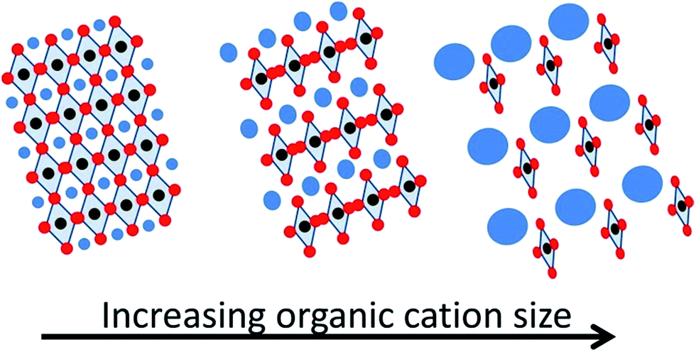 | ||
| Scheme 5 Pictorial illustration of the lattice expansion with the organic cation size. | ||
Additionally, the use of different organic cations (i.e. formamidium, HC(NH2)2+) instead of CH3NH3+ in planar heterojunctions improves the cell performance by showing negligible hysteresis between forward and reverse J–V measurements.5,27,28
Besides moisture sensitivity and the phase transition issue, the need to expand the light absorption towards the NIR region requires the reduction of the perovskite bandgap. The typical hybrid perovskite CH3NH3PbI3 containing methyl ammonium cations possesses a 1.55 eV band gap, being the ideal bandgap estimated between 1.1 and 1.4 eV for a single-junction solar cell.28 The CH3NH3I precursor is typically prepared by the reaction between a CH3NH2 solution in methanol or ethanol and a HI solution in water at low temperature for about 2 h.8
The utilization of other different organic cations could require adaptation of the synthetic method, although the organic halide cation preparation procedure has been used in the majority of the reports.
It is well known that the perovskite band gap is very sensitive to network structure modifications (i.e. deformation, enlargement or tilting). At room temperature, the tetragonal structure in CH3NH3PbI3 is given by the small size of the CH3NH3+ cation. Therefore, the incorporation of a bigger cation is believed to provide a higher symmetry to the perovskite structure and as a consequence, band gap reduction.29
In this regard, Nam-Gyu Park et al. reported the preparation of lead iodide perovskites of ethylamine (CH3CH2NH3PbI3) mixing equimolar solutions of ethylammonium iodide and lead iodide in γ-butyrolactone.30 The CH3CH2NH3I was prepared by reacting an ethylamine solution in methanol with a hydroiodic acid solution in water, analogously to the typical methylammonium iodine preparation. The resulting perovskite presented a 2H structure consisting of PbI6 chains separated one from the other by ethylammonium ions with an orthorhombic phase (see Scheme 2). The larger alkyl chain length in the organic cation does not allow maintaining the 3 D tetragonal AMX3 lattice. As a consequence of the structural change, the perovskite bandgap increased up to 2.2 eV, and the power conversion efficiency using this cation in the lead iodide perovskite was lower than that of the methylammonium based perovskite.30
Similarly, Baikie and co-workers reported a perovskite containing a formamidium cation (HC(NH2)2+, FA+) instead of the methylammonium (CH3NH3+). The ionic radius of FA+ has been reported to be slightly bigger than that of the methylammonium (rformamidium = 0.279 nm), and therefore the estimated formamidium based perovskite bandgap is 1.47 eV, allowing better spectral absorption.31
Pang et al. reported other synthetic routes for the HC(NH2)2I preparation where formamidium acetate and HI reacted in water at 0 °C for 2 h. The as-prepared cation was used to build FAPbI3 devices using a one-step solution process or the two-step dipping methodology. By using the latter method 7.5% efficiency was reported compared to only 3.7% efficiency obtained by the one-step deposition method. The reason for these results seems to be the feasibility of forming phase-pure FAPbI3 following the two-step dipping method.29
In this context, Snaith et al. reported planar heterojunction devices containing this FA+ based perovskite with an average efficiency of 9.7%.28 In this case, the FAI precursor was prepared by dissolving an excess of formamidium acetate in a HI water solution. The halide perovskite was formed by adding an additional small amount of HI to the stoichiometric FAI:PbI2 (1:1) in DMF solution during FAPbI3 formation, observing the absence of the yellow phase after annealing. At the same time, Park et al. reported an improved FAI synthetic route, where high quality FAI was obtained with a yield above 90%.27 The employed synthetic method does not use formamidium acetate as the precursor in order to avoid the formation of acetic acid during the reaction with HI which is not easy to eliminate. Instead of methanol they used ethanol in the presence of sodium hydride since in the formamidium formation, NaCl precipitation is favored due to the lower solubility of this salt in ethanol compared to methanol. Power conversion efficiencies up to 16% were obtained using FAPbI3 perovskite prepared with the optimal precursor. Another additional advantage of this FAPbI3 perovskite is that it does not show phase transition, increasing thermal stability when compared to the parent CH3NH3PbI3.27
Seok et al. explored adequate solvents to form intermediate phases, thus retarding the reaction between PbI2 and FAI. In this approach, the addition of DMSO as a co-solvent to the PbI2 precursor was reported. The DMSO–PbI2 precursor has been reported to promote the formation of more uniform and dense films. Subsequent exchange of DMSO by FA+ cations was efficiently accomplished without structural changes due to their higher affinity for PbI2, which provides highly uniform and dense FAPbI3 films. Photovoltaic devices employing this DMSO–PbI2 precursor and a subsequent intramolecular exchange process presented certified efficiencies exceeding 20%.32
A different approach was explored by Grätzel and co-workers who reported a systematic study on the partial substitution of the methylammonium cation by FA+.33 A maximum power conversion efficiency of 14.9% was obtained by using (CH3NH3)0.6FA0.4PbI3. This combination produced a double benefit since the FA+ cation not only reduced the perovskite bandgap, but also enhanced the light harvesting in the visible region by extending light absorption up to 850 nm. As a consequence, the (CH3NH3)0.6FA0.4PbI3 perovskite based devices achieved photovoltages as high as those obtained for CH3NH3PbI3, but with improved current densities. In a similar way, Han et al. reported a mix of methylammonium and 5-aminovaleric acid cations (H3N(CH2)4CO2H+, AVA+) in the synthesis of the mixed-cation perovskite (5-AVA)x(CH3NH3)1−xPbI3.34 A certified power conversion efficiency of 12.8% was achieved by using this mixed-organic cation perovskite.
In this case, the partial substitution of the methylammonium cation by AVA+ favors an orthorhombic perovskite phase, enhancing the light harvesting without a change in the spectral response, increasing the device photocurrent, and, therefore, the power conversion efficiency.
Recently, Seok et al. reported photovoltaic devices incorporating small proportions of (CH3NH3PbBr3) into (FAPbI3) to obtain (FAPbI3)1−x(CH3NH3PbBr3)x, where x varies from 0 to 0.3.5 The rationale behind this strategy derives from the relative instability reported for FAPbI3 due to the formation of a yellow non-perovskite polymorph (δ-phase) which should be responsible for inefficient charge transport and an increase in the optical bandgap. In contrast, CH3NH3PbBr3 is well known to tune the perovskite band gap up to 2.3 eV as well as to stabilize the perovskite structure. By optimization of the molar ratio between FAPbI3 and CH3NH3PbBr3 to x = 0.15, the authors demonstrated stabilization of the perovskite black phase. The optimized phase stability and crystallinity enhanced the balance between electrons and holes in the perovskite, reducing the cell hysteresis and obtaining an average device efficiency between the reverse and forward applied bias of 18.4% under 1 Sun illumination.5
Although the best device efficiencies have been reported employing organic cations in the ABX3 perovskite structure, some reports have questioned the need for using only organic cations.35 In fact, it has been reported that Cs+ doped CH3NH3PbI3 produced Jsc and Voc improvements, enhancing the overall device efficiencies from 5.5 to 7.7%.36 In this case, CsI was mixed with CH3NH3I in different proportions in order to form the final perovskite (Csx(CH3NH3)1−xPbI3) in the presence of PbI2. The optimum device efficiency was obtained with a doping value of 10% of Cs+. Further increase in Cs+ content produced less efficient devices, not only due to bandgap enhancement, losing the spectral response, but also due to the presence of undesirable crystal phases such as CsI, PbI2 and Cs4PbI6.36
Consideration of the current state of the art shows that there is still interest in testing other small size organic cations besides those containing N, preferably those that could give stable perovskite crystal phases, including in the study the most appropriate synthetic route for high purity perovskite formation and also a suitable film processing protocol. In addition, further understanding of the influence that doping with inorganic alkali metals and related cations can play in the performance of photovoltaic devices based on hybrid perovskites is still necessary.
The metal cation
It is well established that in the general formula (AMX3) of hybrid organic–inorganic halide perovskites M corresponds to a divalent metal cation such as Cu2+, Ni2+, Co2+, Fe2+, Mn2+, Cr2+, Pd2+, Cd2+, Ge2+, Sn2+, Pb2+, Eu2+ or Yb2+.37 The most studied divalent cations in photovoltaics have been Pb2+ and Sn2+, although the most efficient devices have been obtained always using Pb2+. Considering the toxicity of Pb2+, replacement of this heavy metal cation by a less toxic metal that can result in an adequate perovskite bandgap without detriment to the performance of the photovoltaic device is at this moment under intense research. For this reason, group 14 elements with comparable ionic radii to that of Pb2+ have been intensely explored to allow replacement of toxic Pb.Since the discovery of the electrical properties of inorganic oxide perovskites, a large number of compositions have been explored. One of the first reports on the synthesis and characterization of hybrid halide perovskites was carried out by Mitzi and co-workers in 1994.38 They reported one family of hybrid halide perovskites ((C4H9NH3)2(CH3NH3)n−1SnnI3n+1) with very promising electronic properties. Lately, the same author explored the electrical, optical and thermal properties of a series of hybrid halide perovskites (C4H9NH3)2MI4, where M = Ge, Sn or Pb.39 All these perovskites were synthesized from aqueous hydroiodic acid solutions. MI4 (M = Ge, Sn and Pb) precursors were dissolved in aqueous HI solutions and reduced to MI2 by addition of appropriate amounts of H3PO3 into the HI solution (Scheme 6). Afterwards, (C4H9NH3)2·HI solutions in aqueous HI were added to the MI2 solutions resulting in the formation of the desired perovskites that precipitate from the solution. Orthorhombic structures were obtained for all metals; however, (C4H9NH3)2GeI4 presented a different space group and greater distortion in the GeI6 octahedra compared with the perovskites of the other two metals. This distortion produced a lower melting point and smaller bandgap in the (C4H9NH3)2GeI4 perovskite compared to the other two having Sn and Pb as metals.39 Although (C4H9NH3)2GeI4 showed the widest light harvesting ability due to its reduced bandgap, (C4H9NH3)2SnI4 and (C4H9NH3)2PbI4 were more stable structures. The similar ionic radii of Sn2+ 1.35 Å and Pb2+ 1.49 Å result in a lack of significant lattice perturbation in their structures, (C4H9NH3)2PbI4 exhibiting the bigger bandgap.
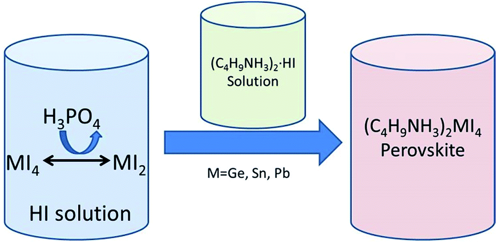 | ||
| Scheme 6 Preparation procedure of hybrid halide perovskites using Ge, Sn or Pb as metals. | ||
Consequently, the interest in avoiding lead due to environmental concerns as well as extending the light harvesting ability to the NIR boosted the use of hybrid halide perovskites with Sn as a divalent metal cation.38,40,41 However, this Sn based perovskite has shown a poor stability in air compared with the Pb based perovskite due to the oxidation of Sn2+ to Sn4+.
Obviously, this oxidation produces structural changes which are reflected in different properties such as metal-like conductivity and the modification of the performance as a p-type semiconductor.42 Recently, Ogomi and co-workers found that a minimal content of Pb atoms in the Sn perovskite is enough to decrease the tendency to undergo oxidation from Sn2+ to Sn4+, thus increasing perovskite stability in air.43 In addition, the mix of divalent metal cations (Sn2+ and Pb2+) allowed bandgap tuning by varying the Sn:Pb ratio (Scheme 7). Thus, solar cells based on CH3NH3Sn0.5Pb0.5I3 perovskite obtained 4.18% efficiency upon 1 Sun illumination and a current density value of 20 mA cm−2 was achieved due to the absorption edge of the material at 1060 nm. On the other hand, Kanatzidis et al. reported that solid solutions of CH3NH3PbI3 and CH3NH3SnI3 perovskites achieved 7.27% efficiency for the CH3NH3Pb0.5Sn0.5I3 composition.44 This sample is synthesised by reprecipitation of appropriate amounts of the two different metal perovskites. The difference between the two procedures for preparation of mixed-metal hybrid perovskites is the synthesis procedure. In one case, CH3NH3I, PbI2 and SnI2 precursors were mixed in stoichiometric proportions to obtain the CH3NH3Sn0.5Pb0.5I3 perovskite, while in the latter case the already prepared CH3NH3PbI3 and CH3NH3SnI3 solids were dissolved together in order to obtain the mixed perovskite with apparently the same composition, but different performance.
 | ||
| Scheme 7 Energy diagram of CH3NH3SnxPb(1−x)I3 perovskite. Reproduced with permission from ref. 43. | ||
Besides the poor air stability observed for the Sn perovskites due to the aerobic Sn2+ oxidation, the other problem responsible for the low power conversion efficiency in photovoltaic devices built with Sn-containing perovskites is the discontinuous film morphology and poor electrode coverage (Fig. 1). The inefficient film coverage is responsible for shorting, poor charge transport and fast charge recombination. In this regard, Jen et al. reported an improved synthetic route to obtain binary Pb–Sn perovskites.45 In this report, an ethanolic solution of methylamine was mixed with an aqueous solution of HI in the presence of hydrophosphorous acid. Then, CH3NH3I, PbCl2 and SnCl2 were mixed in the desired ratio in anhydrous DMF. Planar heterojunction devices were built using CH3NH3Pb1−aSnaI3−xClx were prepared in this way and high electrode coverages (up to 97%) were obtained. In addition, the Sn atom incorporation shifted the absorption from 800 nm to 900 nm, achieving a maximum device efficiency of 10.1% at 1 Sun. This result was obtained with 85:15 Pb:Sn atomic percentage in the perovskite composition, which correlated with the film with the highest electrode coverage as determined by scanning electron microscopy.45
 | ||
| Fig. 1 SEM images of CH3NH3Pbx (right) and CH3NH3Pb0.85Sn0.15X (left) films. Reproduced with permission from ref. 45. | ||
In spite of the enhanced light harvesting in the NIR, and the more than 20 mA cm−2 current density obtained from this Sn/Pb mixed perovskite, the overall efficiency under 100 mW cm−2 of sun simulated light was still lower than the average efficiency of the Pb based hybrid halide perovskite, although single Pd hybrid perovskite absorbs light only up to 800 nm.
A lower open circuit voltage (Voc) and fill factor (FF) are usually obtained with devices containing Sn in the perovskite structure. Therefore, deeper understanding of the charge transfer reactions taking place in the active layer (especially charge separation and recombination) is needed to devise strategies to overcome these limitations and combine in a material the advantages of the enhanced photocurrent obtained with the Sn based perovskite with the high photovoltage exhibited by Pb based perovskite.
In this regard, Shen and co-workers determined that the density of defects and trap states in binary Sn/Pb perovskites was higher than that in Pb based perovskites.46 As a consequence, only 20% of the Sn/Pb based perovskite excited states have lifetime longer than 3 ns (Fig. 2), while, in Pb based perovskite 90% of excitons decayed after 100 ns. This faster excited state deactivation was attributed to nonradiative charge recombination through trap states in the binary perovskite. The authors found it possible to enhance the Voc and FF by defect density reduction in the Sn/Pb perovskites.46 Therefore, composition optimization and engineering of the Sn based perovskite are needed in order to reduce the density of defects and reduce recombination.
 | ||
| Fig. 2 Transient absorption response of Sn/Pb perovskite on the Al2O3 substrate (black: experimental signal; red: best fitting). The inset shows the transient signal for the first 20 ps. Reproduced with permission from ref. 46. | ||
One example of composition engineering can be found in the case of an all inorganic CsSnI3 perovskite with an orthorhombic structure, which has been employed as a solid electrolyte in a dye-sensitized solar cell.47 The typical I−/I3− redox pair in liquid electrolytes can be replaced with this inorganic perovskite, which not only presented improved hole mobility properties, respect to other solid state electrolytes, but also its 1.3 eV bandgap introduces additional photoresponse in the NIR part of the radiation spectra (absorption edge 953 nm). Photovoltaic devices employing this perovskite as the solid electrolyte achieved more than 10% efficiency by doping the perovskite with 5% of F− (CsSnI2.9F5).47 Based on this precedent, CsSnI3 has also been employed as an active material in solar cells with spectral responses up to 950 nm. Nevertheless, efficient photovoltaic devices were only obtained by doping the inorganic perovskite with SnF2. The poor performance without the F− doping was due to the presence of intrinsic defects associated with the Sn metal cation, which results in metallic conductivity. Therefore, the addition of SnF2 was found to be very important in order to reduce background carrier density.48
Theoretical calculations have revealed that the main differences between Sn and Pb based perovskites are a consequence of relativistic effects due to the contraction of valence band atomic orbitals. These effects stabilize significantly Pb based perovskites against oxidation due to the much deeper valence band edge, which at the same time also increases their bandgap.49 In other words, theory indicates that the optimum Sn based perovskite bandgap derives from a relatively elevated valence band that, on the other hand, is also responsible for the easy Sn2+ oxidation.
Other candidates for lead-free perovskites such as (CH3NH3)2CuCl4−xBrx or (RNH3)2FeX4 have been synthesized.50,51 However in these cases 2H structures have been obtained instead of the 3D polymorphs resulting for metals from the 14 group. In the case of the Cu based perovskite the bandgap can be tuned by increasing the ratio of Br in the structure. However, the presence of Cl has been found to be crucial in order to avoid Cu2+ reduction. Although light harvesting in the NIR region has been achieved, efficiencies as low as 0.02% were measured and attributed to the partial Cu2+ reduction by Br−, which introduces anion vacancies acting as charge carrier trapping sites.50 In the case of the Fe based perovskites metal oxidation from Fe2+ to Fe3+ has been identified as a possible source of instability, and there are still no optoelectronic studies showing the photovoltaic activity of Fe hybrid halide perovskites in spite of their obvious interest derived from abundance and the lack of toxicity of Fe.7
The synthesis and crystallographic characterization of NH3(C6H4)2NH3CuCl4 and NH3(C6H4)2NH3HgCl4 organic–inorganic perovskites have been also reported.52 The Cu based perovskite structure showed well-ordered sheets of corner-sharing distorting CuCl6 octahedra, separated by layers of the organic cation. However, the Hg based perovskite presented anionic parallel layers and alternating layers of the organic cation and tetrahedral HgCl42−. In both cases, the different organic–inorganic layers are interconnected by relatively weak H-bonds between amino groups of organic cations and the Cl− of the anionic counterparts,52 making them good candidates to explore their photovoltaic performance or for the synthesis of similar structures containing organic cations with different compositions and sizes.
In this regard, Papavassiliou et al. reported a complete structural, optical and electronic study of organic–inorganic semiconductors using combinations of a wide range of organic cations and metal halides (M = Bi, Sb, Sn, Pb, Cu and Ag),53 opening the possibility to explore the use of metal alternatives to Pb.
The inorganic anion
As commented earlier, many perovskites of different compositions have been described in the literature (oxides, nitrides or halides). However, hybrid halide perovskites have been found to exhibit the best optoelectronic properties. In this regard, the influence of the halogen elements I, Cl and Br, and their combinations has been widely studied and a strong dependence of the photovoltaic performance of the perovskite cell depending on the halogen composition has been demonstrated.It was reported in 2003 that CH3NH3PbBr3 presented a larger bandgap and tighter bound excitons than CH3NH3PbI3 as a consequence of the intrinsic properties of each halogen.54 Exciton binding energies of 76 meV and 50 meV were estimated for CH3NH3PbBr3 and CH3NH3PbI3, respectively, which are larger than the exciton binding energy of other inorganic semiconductors such as GaAs (4.2 meV).55 This was lately confirmed in perovskite solar cells, where the hybrid halide perovskites CH3NH3PbI3 and CH3NH3PbBr3 were compared using liquid electrolytes.1 The power conversion efficiencies of CH3NH3PbI3 and CH3NH3PbBr3 were 3.81% and 3.18%, respectively. However, to put these efficiency values in perspective it has to be considered that perovskites containing I showed a smaller bandgap than perovskites containing Br. Therefore, in the incident photon to current efficiency (IPCE) measurements, it was determined that devices based on CH3NH3PbI3 harvested light up to 800 nm, while in CH3NH3PbBr3 devices light harvesting occurs below 600 nm. When corrected for this difference in light absorption, the differences in IPCE values are very minor. In addition, photoelectron spectroscopy determined that the CH3NH3PbI3 valence band (5.44 eV) is higher in energy than the CH3NH3PbBr3 valence band (5.38 eV) and conduction band edges calculated from the valence band and the optical bandgap were estimated to be at 3.36 eV for CH3NH3PbBr3 and 4 eV for CH3NH3PbI3.1 The origin of the Voc in perovskite based photovoltaic devices still remains unclear and it is under discussion. Although active materials showing larger band gaps should, in principle, lead to devices with higher Voc than smaller band gaps materials due to the energy difference between their conduction and valence bands, the redox potential of organic hole conductors and the work function of the different electrodes used in device construction, together with internal resistance, limit the observed Voc in devices. The recombination rate plays a key role in the performance not only in perovskite solar cells but also in other types of photovoltaic devices such as dye sensitized solar cells or organic solar cells. Recombination dynamics has been found to be composition-dependent in perovskite solar cells, and the addition of a small percentage of Br− into mixed halides perovskite solar cells has been found to reduce the recombination rate when compared to the pure materials.56
The high band gap in CH3NH3PbBr3 perovskites allows the possibility to build high Voc solar cells, which could offer opportunities in electrochemical reactions,57,58 tandem cells59 or photodetectors.60 In this sense Qiu and co-workers reported hybrid CH3NH3PbBr3 perovskite solar cells exhibiting 1.15 V at open circuit using poly[N-9-heptadecanyl-2,7-carbazole-alt-3,6-bis-(thiophen-5-yl)-2,5-dioctyl-2,5-di-hydropyrrolo[3,4]pyrrole-1,4-dione] (PCBTDPP) as a hole conductor. Similarly, others reports have appeared showing the use of different hole conductors in CH3NH3PbBr3 perovskite solar cells in order to maximize the open circuit voltage up to 1.4 V.61,62
In spite of the high open circuit voltages obtained with the Br perovskite and the reported organic hole conductors, the overall efficiencies obtained at 1 Sun illumination in such devices were far from the average efficiency obtained using I as an inorganic anion in the perovskite. This low efficiency makes difficult the application of bromide-based perovskite in the production of solar fuels or tandem cells. However, Im et al. reported that one of the reasons for such a low efficiency could be a low density of CH3NH3PbBr3 films, and therefore, poor electrode coverage.63 They found that CH3NH3PbBr3 perovskite dissolved in DMF produced fast nucleation of isolated CH3NH3PbBr3 crystals, which produced low coverage and inefficient devices. However, when they added HBr aqueous solution to the CH3NH3PbBr3 perovskite in DMF the crystal nucleation slowed down, due to the improved solubility of CH3NH3PbBr3 in the solvent mix, resulting in the formation of denser and thinner films with full coverage. Using the DMF/HBr solvent and the organic hole conductor PIF8-TAA, 10.4% efficiency at 1 Sun illumination was obtained, exhibiting 1.5 V in open circuit.63 Recently, a vapor-assisted method for CH3NH3PbBr3 fabrication has been utilized as an alternative to overcome the poor film coverage that solution methods present. A PbBr2 film, previously deposited by spin coating, was treated with CH3NH3Br vapor at 150 °C for 10 min. This procedure allowed densely packed grains and full film coverage on a transparent electrode which produced 8.7% efficiency with 1.45 Voc at 1 Sun.64
Theoretical calculations have determined that defects in CH3NH3PbBr3 are predominantly shallow traps,65 suggesting negligible losses due to non-radiative recombination pathways. These calculations are in agreement with the observation of the high open circuit voltages in CH3NH3PbBr3 perovskite solar cells. However, these calculations indicate that CH3NH3PbBr3 should exhibit only unipolar behavior and, therefore, it can only act as a p-type semiconductor in contrast to the CH3NH3PbI3, which shows bipolar behavior. Therefore, the less efficient electron transport determines that optimal CH3NH3PbBr3 perovskite films have to be thinner than CH3NH3PbI3 for balanced electron/hole extraction, losing under these conditions light harvesting ability. Thus, a compromise between light absorption and the optimal film thickness appears to be crucial for the best performing CH3NH3PbBr3 perovskite cell. Poor charge migration should be responsible for enhanced charge recombination in CH3NH3PbBr3 compared with CH3NH3PbI3 perovskite solar cells. Nevertheless, CH3NH3PbBr3 has been proposed as a good candidate for the top cells in tandem solar cells, being an excellent additive for light harvesting in other perovskite solar cells to achieve high photovoltage, as well as for hole transport.65
The CH3NH3PbCl3 perovskite presents an even higher bandgap (3.11 eV) than CH3NH3PbBr3 perovskites (2.3 eV) and CH3NH3PbI3 (1.55 eV). For that reason CH3NH3PbCl3 cannot be used as a light harvesting material. However, the use of mixed halide perovskites appears as a promising approach to tune the optoelectronic properties of single halide perovskites, improving the photovoltaic performance of single-halide perovskite solar cells. The incorporation of mixed halide anions into the structure of the archetypical CH3NH3PbI3 hybrid perovskite has been found to affect the charge recombination dynamics in the photovoltaic devices. Mora-Sero et al. determined that the incorporation of Cl− or Br− into the perovskite structure slows down recombination kinetics, increasing the Voc. In addition, the presence of Br improved the device stability.56 Nevertheless, the role of Cl anions and how many of them remain in the final structure of the mixed halide perovskite are still under discussion.66,67 In any case, incorporation of Cl− into the composition of perovskite solar cells has proved to extend the charge diffusion length without changing the spectral response, although only a small percentage of Cl atoms can be tolerated in the perovskite lattice.
In 2012, Snaith et al. reported the use of a CH3NH3PbI3−xClx perovskite using either TiO2 or Al2O3 as an n-type component or scaffold, respectively.2 They found that devices using an Al2O3 mesoporous layer were more efficient than those using TiO2, mainly due to the faster electron transport in the mixed perovskite when Al2O3 was used instead of TiO2. Apart from device structural considerations, they found that the crystallization rate can be controlled by changing the halide composition. The inclusion of Cl atoms replacing a percentage of I produced a longer crystallization process as a consequence of lattice distortion generated by the Cl inclusion in the perovskite structure. Moreover, I anion substitution by Cl was again found to increase the electron conductivity and charge diffusion length. These beneficial effects seem to be not counterbalanced by important negative side effects in the film since spectroscopic measurements have shown similar light harvesting (from 400 to 800 nm) for NH3NH3PbI3−xClx compared to the parent CH3NH3PbI3 perovskite solar cells, indicating no change in bandgap (1.55 eV) despite the incorporation of Cl into the perovskite lattice. The use of the mixed halide CH3NH3PbI3−xClx not only produces a remarkable enhancement in the film conductivity, but also improves the morphology of the films in comparison with those of CH3NH3PbI3 devices processed under the same conditions. Other additional benefits are the reduction of the J–V hysteresis and an improvement in the device reproducibility.68,69
Crystallization is an important process controlling the overall photovoltaic cell performance that depends on multiple variables such as precursor composition, concentration, solvents and deposition temperature. In this regard, highly dense films of mixed halide perovskite CH3NH3PbI3−xClx have been deposited via the solution processing method resulting in highly reproducible photovoltaic devices with efficiencies up to 10.8%.70 These dense films were achieved by increasing the mixed halide perovskite precursor concentrations and optimizing film deposition conditions by controlling the spin rate. Both modifications were carried out by using dimethyl sulfoxide (DMSO) as the solvent, since compared with DMF or mixed DMF and γ-butyrolactone, DMSO allows preparation of more concentrated CH3NH3PbI3−xClx precursors (up to 60 wt%). In addition, DMSO possesses a higher boiling point which is advantageous for achieving a slower drying.70 Other approaches employed to control the crystal growth in solution processed mixed halide perovskites are based on the use of additives (such as 1,8-diiodooctane) in the precursor solutions.71
The formation of flat uniform films of CH3NH3PbI3−xClx using a dual-source vapor deposition method has been also demonstrated by Snaith et al.14 In this way, planar heterojunction photovoltaic devices were prepared, demonstrating 15% efficiency at 1 Sun, without the need for using solvents and subsequent drying. Using this preparation method, an orthorhombic structure of high crystal quality was reported, having in the XRD pattern smaller peaks attributable to PbI2, in contrast to the patterns obtained from solution processing methods. In addition, no peaks corresponding to CH3NH3PbCl3 were found.
Besides I and Cl mixed halide perovskites, other halide mixtures have been tested in perovskite solar cells. For example, CH3NH3PbI2Br has been deposited on TiO2 nanowires and compared with the CH3NH3PbI3 perovskite in photovoltaic devices. The Br introduction into the perovskite lattice produced a higher absorption coefficient and shifted the conduction band to higher energy values. As a consequence, both the power conversion efficiency and open circuit voltage of the mixed halide perovskite were improved in comparison with the parent CH3NH3PbI3 perovskite devices.72 In fact, Seok et al. tuned the optical and electronic properties of CH3NH3Pb(I1−xBrx)3 by composition engineering. They controlled the perovskite bandgap over almost the complete visible region, changing the I/Br ratio, and obtaining 12.3% power conversion for the most efficient photovoltaic devices containing a mixed halide perovskite with x = 0.2.73
As commented earlier, the CH3NH3PbBr3 perovskite is a wide bandgap material with excellent hole conducting properties. Therefore, this perovskite has been used in combination with CH3NH3PbI3 in order to obtain, on one hand, tunable bandgap perovskite, and on the other hand, free hole conductor perovskite solar cells.74
High voltage perovskite solar cells have been reported using the mixed halide perovskite CH3NH3PbBr3−xClx.75 The inclusion of Cl anions in the CH3NH3PbBr3 perovskite produced not only an enhancement in the Voc, but also in Jsc. Thus, values of 1.5 V and 4 mA cm−2 were observed for this CH3NH3PbBr3−xClx perovskite upon 100 mW cm−2 irradiation at 1 Sun. The enhanced Voc and Jsc with respect to the Br− only based perovskite were attributed to an improved film coverage caused by the presence of the Cl− anions, increasing in this way the light absorption and decreasing losses due to shorting. It was observed that the presence of Cl− produces smaller crystallites, which results in a denser perovskite layer.75 Actually, crystallization studies have determined that the inclusion of PbCl2 during the formation of both CH3NH3PbI3 and CH3NH3PbBr3 perovskites has a beneficial effect on the quality of the final perovskite layers since PbCl2 crystals act as nucleation points during perovskite formation due to its low solubility in DMF that is the common solvent used. PbCl2 activity as seeds results in more dense layers for both I and Br perovskites obtained when PbCl2 is added.76
Apart from Cl and Br anions, F− has been also incorporated into the structure of mixed halide perovskites by Nagane and co-workers.77 They reported the partial substitution of I− by BF4− anions, which present a similar ionic radius. It was reported before that the stability of the perovskite structure decreases from I− to F−, making the formation of stable F− and I− mixed halide perovskites really difficult.78 However, the preparation of CH3NH3PbI(3−x)(BF4)x through chemical vapor deposition of the prepared CH3NH3BF4 on PbI2 films produced tetragonal crystal structures identical to the typical CH3NH3PbI3. The incorporation of F atoms into the BF4− anion produced an enhanced conductivity in the perovskite films. This was explained in terms of the higher electronegativity and electron withdrawing behavior of F compared with the other halides. Besides, the F− radius is smaller than that of I−; therefore the substitution of I− directly by F− rather than by BF4− should result, in the case of Pb, in strong lattice deformation resulting in detrimental optoelectronic consequences. However, the incorporation of the F atoms into the BF4− anion, with a similar ionic radius to I−, avoids this lattice distortion and induces improved electrical conductivity, maintaining an absorption edge at 760 nm.77
Conclusions
Perovskite solar cells have abruptly emerged in the photovoltaic field due to the high power conversion efficiency they demonstrated in just few years. This breakthrough in the photovoltaic field is a consequence, on one hand, of the considerable structural and chemical knowledge of hybrid perovskites that started decades ago by Weber,79 and lately, the study of their physical properties by Mitzi.37–40 On the other hand, the technological advances in the preparation of films and deposition methods, already developed for other photovoltaic technologies, have been adapted in a straightforward manner for the preparation of perovskite solar cells.CH3NH3PbI3 perovskite solar cells have demonstrated impressive record device efficiencies, and almost introduction in the commercial market has already been informed.80 The now-a-days efficiency is getting close to the theoretical maximum value (∼31%), which is close to the Shockley and Queisser limit of 33%.81 This theoretical limit predicts a maximum Jsc of 26 mA cm−2 and Voc of 1.3 V, approximately.82 Nevertheless, some open questions and concerns still require further research and developments such as the origin of the hysteresis effect in the J–V curves measurements, which causes doubts in the accuracy of the efficiency measurements, the need for lead-free perovskites to avoid the use of this toxic heavy metal and the long-term stability demonstration of such photovoltaic technology.
In this regard, variation of the chemical composition of the hybrid halide perovskites can be a suitable methodology for finding an adequate solution for these three targets. The substitution of the typical methylammonium organic cation has been proved to extend light absorption into the NIR region, enhancing at the same time the crystal phase and material stability. The search for new organic or even inorganic cations with similar radii to that of the ammonium cation could open new possibilities to improve even further the optoelectronic performance that hybrid perovskites have shown so far. Moreover, it has been demonstrated that the partial substitution of the Pb cation by Sn, besides reducing the amount of undesirable Pb toxic metal, is able to allow certain bandgap tuning, achieving absorption edge up to 1060 nm. The search for new metal cations with similar properties to those corresponding to the 14 group is still open, and some perovskites containing Cu or Fe have been already prepared, although the currently available performance data are far from optimal. Finally, the use of mixed halide perovskites has been found to improve film coverage, allowing also tuning of the perovskite bandgap, disfavoring charge recombination events and even improving stability. Nonetheless, not only halides must be tested in photovoltaic applications, but also other counter anions susceptible to form perovskite structures (as nitrates or oxides) should be tested in order to achieve higher device stability and efficiencies that currently limit the commercial application of hybrid perovskite photovoltaic solar cells.
Acknowledgements
Financial support by the Spanish Ministry of Economy and Competitiveness (Severo Ochoa and CTQ2015-69153-C2-1-R) and Generalidad Valenciana (Prometeo 2013/014) is gratefully acknowledged.References
- A. Kojima, K. Teshima, Y. Shirai and T. Miyasaka, J. Am. Chem. Soc., 2009, 131, 6050–6051 CrossRef CAS PubMed.
- M. M. Lee, J. Teuscher, T. Miyasaka, T. N. Murakami and H. J. Snaith, Science, 2012, 338, 643–647 CrossRef CAS PubMed.
- H. Zhou, Q. Chen, G. Li, S. Luo, T.-b. Song, H.-S. Duan, Z. Hong, J. You, Y. Liu and Y. Yang, Science, 2014, 345, 542–546 CrossRef CAS PubMed.
- National Renewable Energy Labs (NREL) Efficiency Chart.
- N. J. Jeon, J. H. Noh, W. S. Yang, Y. C. Kim, S. Ryu, J. Seo and S. I. Seok, Nature, 2015, 517, 476–480 CrossRef CAS PubMed.
- S. D. Stranks, P. K. Nayak, W. Zhang, T. Stergiopoulos and H. J. Snaith, Angew. Chem., Int. Ed., 2015, 54, 3240–3248 CrossRef CAS PubMed.
- P. P. Boix, S. Agarwala, T. M. Koh, N. Mathews and S. G. Mhaisalkar, J. Phys. Chem. Lett., 2015, 6, 898–907 CrossRef CAS PubMed.
- S. Luo and W. A. Daoud, J. Mater. Chem. A, 2015, 3, 8992–9010 CAS.
- V. M. Burlakov, G. E. Eperon, H. J. Snaith, S. J. Chapman and A. Goriely, Appl. Phys. Lett., 2014, 104, 091602 CrossRef.
- N.-G. Park, Mater. Today, 2015, 18, 65–72 CrossRef CAS.
- G. E. Eperon, V. M. Burlakov, P. Docampo, A. Goriely and H. J. Snaith, Adv. Funct. Mater., 2014, 24, 151–157 CrossRef CAS.
- E. L. Unger, E. T. Hoke, C. D. Bailie, W. H. Nguyen, A. R. Bowring, T. Heumuller, M. G. Christoforo and M. D. McGehee, Energy Environ. Sci., 2014, 7, 3690–3698 CAS.
- T. Leijtens, B. Lauber, G. E. Eperon, S. D. Stranks and H. J. Snaith, J. Phys. Chem. Lett., 2014, 5, 1096–1102 CrossRef CAS PubMed.
- M. Liu, M. B. Johnston and H. J. Snaith, Nature, 2013, 501, 395–398 CrossRef CAS PubMed.
- N. J. Jeon, J. H. Noh, Y. C. Kim, W. S. Yang, S. Ryu and S. I. Seok, Nat. Mater., 2014, 13, 897–903 CrossRef CAS PubMed.
- N. Ahn, D.-Y. Son, I.-H. Jang, S. M. Kang, M. Choi and N.-G. Park, J. Am. Chem. Soc., 2015, 137, 8696–8699 CrossRef CAS PubMed.
- D. Liu and T. L. Kelly, Nat. Photonics, 2014, 8, 133–138 CrossRef CAS.
- Q. Chen, H. Zhou, Z. Hong, S. Luo, H.-S. Duan, H.-H. Wang, Y. Liu, G. Li and Y. Yang, J. Am. Chem. Soc., 2014, 136, 622–625 CrossRef CAS PubMed.
- Z. Xiao, C. Bi, Y. Shao, Q. Dong, Q. Wang, Y. Yuan, C. Wang, Y. Gao and J. Huang, Energy Environ. Sci., 2014, 7, 2619–2623 CAS.
- J. Burschka, N. Pellet, S.-J. Moon, R. Humphry-Baker, P. Gao, M. K. Nazeeruddin and M. Gratzel, Nature, 2013, 499, 316–319 CrossRef CAS PubMed.
- Y. Zhao and K. Zhu, J. Phys. Chem. Lett., 2014, 5, 4175–4186 CrossRef CAS PubMed.
- J. J. Choi, X. Yang, Z. M. Norman, S. J. L. Billinge and J. S. Owen, Nano Lett., 2014, 14, 127–133 CrossRef CAS PubMed.
- L. Zheng, D. Zhang, Y. Ma, Z. Lu, Z. Chen, S. Wang, L. Xiao and Q. Gong, Dalton Trans., 2015, 44, 10582–10593 RSC.
- T. Baikie, Y. Fang, J. M. Kadro, M. Schreyer, F. Wei, S. G. Mhaisalkar, M. Graetzel and T. J. White, J. Mater. Chem. A, 2013, 1, 5628–5641 CAS.
- G. Kieslich, S. Sun and A. K. Cheetham, Chem. Sci., 2014, 5, 4712–4715 RSC.
- A. Amat, E. Mosconi, E. Ronca, C. Quarti, P. Umari, M. K. Nazeeruddin, M. Grätzel and F. De Angelis, Nano Lett., 2014, 14, 3608–3616 CrossRef CAS PubMed.
- J.-W. Lee, D.-J. Seol, A.-N. Cho and N.-G. Park, Adv. Mater., 2014, 26, 4991–4998 CrossRef CAS PubMed.
- G. E. Eperon, S. D. Stranks, C. Menelaou, M. B. Johnston, L. M. Herz and H. J. Snaith, Energy Environ. Sci., 2014, 7, 982–988 CAS.
- S. Pang, H. Hu, J. Zhang, S. Lv, Y. Yu, F. Wei, T. Qin, H. Xu, Z. Liu and G. Cui, Chem. Mater., 2014, 26, 1485–1491 CrossRef CAS.
- J.-H. Im, J. Chung, S.-J. Kim and N.-G. Park, Nanoscale Res. Lett., 2012, 7, 353 CrossRef PubMed.
- T. M. Koh, K. Fu, Y. Fang, S. Chen, T. C. Sum, N. Mathews, S. G. Mhaisalkar, P. P. Boix and T. Baikie, J. Phys. Chem. C, 2014, 118, 16458–16462 CAS.
- W. S. Yang, J. H. Noh, N. J. Jeon, Y. C. Kim, S. Ryu, J. Seo and S. I. Seok, Science, 2015, 348, 1234–1237 CrossRef CAS PubMed.
- N. Pellet, P. Gao, G. Gregori, T.-Y. Yang, M. K. Nazeeruddin, J. Maier and M. Grätzel, Angew. Chem., Int. Ed., 2014, 53, 3151–3157 CrossRef CAS PubMed.
- A. Mei, X. Li, L. Liu, Z. Ku, T. Liu, Y. Rong, M. Xu, M. Hu, J. Chen, Y. Yang, M. Grätzel and H. Han, Science, 2014, 345, 295–298 CrossRef CAS PubMed.
- M. Kulbak, D. Cahen and G. Hodes, J. Phys. Chem. Lett., 2015, 2452–2456 CrossRef CAS PubMed.
- H. Choi, J. Jeong, H.-B. Kim, S. Kim, B. Walker, G.-H. Kim and J. Y. Kim, Nano Energy, 2014, 7, 80–85 CrossRef CAS.
- D. B. Mitzi, in Progress in Inorganic Chemistry, John Wiley & Sons, Inc., 2007, pp. 1–121 Search PubMed.
- D. B. Mitzi, C. A. Feild, W. T. A. Harrison and A. M. Guloy, Nature, 1994, 369, 467–469 CrossRef CAS.
- D. B. Mitzi, Chem. Mater., 1996, 8, 791–800 CrossRef CAS.
- D. B. Mitzi, S. Wang, C. A. Feild, C. A. Chess and A. M. Guloy, Science, 1995, 267, 1473–1476 CrossRef CAS PubMed.
- N. K. Noel, S. D. Stranks, A. Abate, C. Wehrenfennig, S. Guarnera, A.-A. Haghighirad, A. Sadhanala, G. E. Eperon, S. K. Pathak, M. B. Johnston, A. Petrozza, L. M. Herz and H. J. Snaith, Energy Environ. Sci., 2014, 7, 3061–3068 CAS.
- C. C. Stoumpos, C. D. Malliakas and M. G. Kanatzidis, Inorg. Chem., 2013, 52, 9019–9038 CrossRef CAS PubMed.
- Y. Ogomi, A. Morita, S. Tsukamoto, T. Saitho, N. Fujikawa, Q. Shen, T. Toyoda, K. Yoshino, S. S. Pandey, T. Ma and S. Hayase, J. Phys. Chem. Lett., 2014, 5, 1004–1011 CrossRef CAS PubMed.
- F. Hao, C. C. Stoumpos, R. P. H. Chang and M. G. Kanatzidis, J. Am. Chem. Soc., 2014, 136, 8094–8099 CrossRef CAS PubMed.
- F. Zuo, S. T. Williams, P.-W. Liang, C.-C. Chueh, C.-Y. Liao and A. K. Y. Jen, Adv. Mater., 2014, 26, 6454–6460 CrossRef CAS PubMed.
- Q. Shen, Y. Ogomi, J. Chang, T. Toyoda, K. Fujiwara, K. Yoshino, K. Sato, K. Yamazaki, M. Akimoto, Y. Kuga, K. Katayama and S. Hayase, J. Mater. Chem. A, 2015, 3, 9308–9316 CAS.
- I. Chung, B. Lee, J. He, R. P. H. Chang and M. G. Kanatzidis, Nature, 2012, 485, 486–489 CrossRef CAS PubMed.
- M. H. Kumar, S. Dharani, W. L. Leong, P. P. Boix, R. R. Prabhakar, T. Baikie, C. Shi, H. Ding, R. Ramesh, M. Asta, M. Graetzel, S. G. Mhaisalkar and N. Mathews, Adv. Mater., 2014, 26, 7122–7127 CrossRef CAS PubMed.
- P. Umari, E. Mosconi and F. De Angelis, Sci. Rep., 2014, 4, 04467 Search PubMed.
- D. Cortecchia, H. Arianita Dewi, D. Sabba, T. Baikie, C. Soci and N. Mathews, in EOSAM 2014, European Optical Society, Berlin, 2014 Search PubMed.
- M. F. Mostafa, M. A. Semary and M. A. Ahmed, Phys. Lett. A, 1977, 61, 183–184 CrossRef.
- M. Belhouchet, W. Wamani and T. Mhiri, IOP Conf. Ser.: Mater. Sci. Eng., 2010, 13, 012039 CrossRef.
- G. C. Papavassiliou, G. A. Mousdis and I. B. Koutselas, Adv. Mater. Opt. Electron., 1999, 9, 265–271 CrossRef CAS.
- K. Tanaka, T. Takahashi, T. Ban, T. Kondo, K. Uchida and N. Miura, Solid State Commun., 2003, 127, 619–623 CrossRef CAS.
- S. B. Nam, D. C. Reynolds, C. W. Litton, R. J. Almassy, T. C. Collins and C. M. Wolfe, Phys. Rev. B: Solid State, 1976, 13, 761–767 CrossRef CAS.
- B. Suarez, V. Gonzalez-Pedro, T. S. Ripolles, R. S. Sanchez, L. Otero and I. Mora-Sero, J. Phys. Chem. Lett., 2014, 5, 1628–1635 CrossRef CAS PubMed.
- T. Hisatomi, J. Kubota and K. Domen, Chem. Soc. Rev., 2014, 43, 7520–7535 RSC.
- M. G. Walter, E. L. Warren, J. R. McKone, S. W. Boettcher, Q. Mi, E. A. Santori and N. S. Lewis, Chem. Rev., 2010, 110, 6446–6473 CrossRef CAS PubMed.
- S. Rühle, A. Segal, A. Vilan, S. R. Kurtz, L. Grinis, A. Zaban, I. Lubomirsky and D. Cahen, J. Renewable Sustainable Energy, 2009, 1, 013106 CrossRef.
- G. Konstantatos, I. Howard, A. Fischer, S. Hoogland, J. Clifford, E. Klem, L. Levina and E. H. Sargent, Nature, 2006, 442, 180–183 CrossRef CAS PubMed.
- E. Edri, S. Kirmayer, D. Cahen and G. Hodes, J. Phys. Chem. Lett., 2013, 4, 897–902 CrossRef CAS PubMed.
- S. Ryu, J. H. Noh, N. J. Jeon, Y. Chan Kim, W. S. Yang, J. Seo and S. I. Seok, Energy Environ. Sci., 2014, 7, 2614–2618 CAS.
- J. H. Heo, D. H. Song and S. H. Im, Adv. Mater., 2014, 26, 8179–8183 CrossRef CAS PubMed.
- R. Sheng, A. Ho-Baillie, S. Huang, S. Chen, X. Wen, X. Hao and M. A. Green, J. Phys. Chem. C, 2015, 119, 3545–3549 CAS.
- T. Shi, W.-J. Yin, F. Hong, K. Zhu and Y. Yan, Appl. Phys. Lett., 2015, 106, 103902 CrossRef.
- M. Gratzel, Nat. Mater., 2014, 13, 838–842 CrossRef CAS PubMed.
- S. A. Bretschneider, J. Weickert, J. A. Dorman and L. Schmidt-Mende, APL Mater., 2014, 2, 040701 CrossRef.
- S. Dharani, H. A. Dewi, R. R. Prabhakar, T. Baikie, C. Shi, D. Yonghua, N. Mathews, P. P. Boix and S. G. Mhaisalkar, Nanoscale, 2014, 6, 13854–13860 RSC.
- Q. Chen, H. Zhou, Y. Fang, A. Z. Stieg, T.-B. Song, H.-H. Wang, X. Xu, Y. Liu, S. Lu, J. You, P. Sun, J. McKay, M. S. Goorsky and Y. Yang, Nat. Commun., 2015, 6, 7269 CrossRef CAS PubMed.
- B. Conings, L. Baeten, C. De Dobbelaere, J. D'Haen, J. Manca and H.-G. Boyen, Adv. Mater., 2014, 26, 2041–2046 CrossRef CAS PubMed.
- P.-W. Liang, C.-Y. Liao, C.-C. Chueh, F. Zuo, S. T. Williams, X.-K. Xin, J. Lin and A. K. Y. Jen, Adv. Mater., 2014, 26, 3748–3754 CrossRef CAS PubMed.
- J. Qiu, Y. Qiu, K. Yan, M. Zhong, C. Mu, H. Yan and S. Yang, Nanoscale, 2013, 5, 3245–3248 RSC.
- J. H. Noh, S. H. Im, J. H. Heo, T. N. Mandal and S. I. Seok, Nano Lett., 2013, 13, 1764–1769 CrossRef CAS PubMed.
- S. Aharon, B. E. Cohen and L. Etgar, J. Phys. Chem. C, 2014, 118, 17160–17165 CAS.
- E. Edri, S. Kirmayer, M. Kulbak, G. Hodes and D. Cahen, J. Phys. Chem. Lett., 2014, 5, 429–433 CrossRef CAS PubMed.
- Y. Tidhar, E. Edri, H. Weissman, D. Zohar, G. Hodes, D. Cahen, B. Rybtchinski and S. Kirmayer, J. Am. Chem. Soc., 2014, 136, 13249–13256 CrossRef CAS PubMed.
- S. Nagane, U. Bansode, O. Game, S. Chhatre and S. Ogale, Chem. Commun., 2014, 50, 9741–9744 RSC.
- E. Mosconi, A. Amat, M. K. Nazeeruddin, M. Grätzel and F. De Angelis, J. Phys. Chem. C, 2013, 117, 13902–13913 CAS.
- D. Weber, Z. Naturforsch., B: Anorg. Chem., Org. Chem., 1978, 33, 1443–1445 Search PubMed.
- http://optics.org/news/6/6/21, Imec presents perovskite photovoltaic module with 8% power conversion efficiency.
- W. Shockley and H. J. Queisser, J. Appl. Phys., 1961, 32, 510–519 CrossRef CAS.
- W. E. I. Sha, X. Ren, L. Chen and W. C. H. Choy, Appl. Phys. Lett., 2015, 106, 221104 CrossRef.
| This journal is © The Royal Society of Chemistry 2016 |