
 Open Access Article
 This Open Access Article is licensed under a
 Creative Commons Attribution 3.0 Unported Licence
Anodically fabricated TiO2–SnO2 nanotubes and their application in lithium ion batteries†
M.
Madian
*abc,
M.
Klose
ad,
T.
Jaumann
a,
A.
Gebert
a,
S.
Oswald
a,
N.
Ismail
c,
A.
Eychmüller
b,
J.
Eckert‡
ad and
L.
Giebeler
ad
aLeibniz-Institute for Solid State and Materials Research (IFW) Dresden e.V., Institute for Complex Materials, Helmholtzstr. 20, D-01069 Dresden, Germany. E-mail: m.madian@ifw-dresden.de; mmadian2@gmail.com
bTechnische Universität Dresden, Physical Chemistry, Bergstr. 66b, D-01069 Dresden, Germany
cNational Research Centre, Physical Chemistry Department, 33 El-Buhouth St., 12311 Dokki, Giza, Egypt
dTechnische Universität Dresden, Institut für Werkstoffwissenschaft, Helmholtzstr. 7, D-01069 Dresden, Germany
First published on 9th March 2016
Abstract
Developing novel electrode materials is a substantial issue to improve the performance of lithium ion batteries. In the present study, single phase Ti–Sn alloys with different Sn contents of 1 to 10 at% were used to fabricate Ti–Sn–O nanotubes via a straight-forward anodic oxidation step in an ethylene glycol-based solution containing NH4F. Various characterization tools such as SEM, EDXS, TEM, XPS and Raman spectroscopy were used to characterize the grown nanotube films. Our results reveal the successful formation of mixed TiO2/SnO2 nanotubes in the applied voltage range of 10–40 V. The as-formed nanotubes are amorphous and their dimensions are precisely controlled by tuning the formation voltage which turns Ti–Sn–O nanotubes into highly attractive materials for various applications. As an example, the Ti–Sn–O nanotubes offer promising properties as anode materials in lithium ion batteries. The electrochemical performance of the grown nanotubes was evaluated against a Li/Li+ electrode at a current density of 504 μA cm−2. The results demonstrate that TiO2/SnO2 nanotubes prepared at 40 V on a TiSn1 alloy substrate display an average 1.4 fold increase in areal capacity with excellent cycling stability over more than 400 cycles compared to the pure TiO2 nanotubes fabricated and tested under identical conditions. This electrode was tested at current densities of 50, 100, 252, 504 and 1008 μA cm−2 exhibiting average capacities of 780, 660, 490, and 405 μA cm−2 (i.e. 410, 345, 305 and 212 mA h g−1), respectively. The remarkably improved electrochemical performance is attributed to enhanced lithium ion diffusion which originates from the presence of SnO2 nanotubes and the high surface area of the mixed oxide tubes. The TiO2/SnO2 electrodes retain their original tubular structure after electrochemical cycling with only slight changes in their morphology.
Introduction
The growing rate in green electricity production from renewable energy sources as well as the widespread use of portable electronics and electric vehicles (EVs) has created an urgent need for efficient rechargeable batteries. Lithium ion battery systems offer established techniques related to long cycle life, high energy density, reasonable production cost and the ease of manufacturing flexible designs.1,2 These properties play a central role in the miniaturization of portable electronics and medical devices. Indeed, developing anode materials for lithium ion batteries with higher performance and competitive price compared to graphite represents the bottleneck, although graphite suffers from hazardous dendrite formation, severe solid-electrolyte-interface (SEI) formation, and a relatively large volume expansion of up to 10%.3TiO2-based anodes are alternative materials to overcome the graphite problems owing to their high structural stability obtained from their low volume change during cycling (≈4%), excellent capacity retention, and fast kinetics for lithium intercalation/extraction.4 Furthermore, lithium dendrite and SEI formation are unlikely due to the higher delithiation potential turning TiO2 into a safe operating anode material. On top of that, they are highly abundant and obtained at reasonable production costs.5 Nevertheless, the low theoretical capacity of TiO2 (335 mA h g−1) as well as its poor ionic and electric conductivity represent the main problems to produce high-performance LIBs from titania.4,6,7 To date, research has been focused on two strategies to overcome these problems. The first strategy aims to improve lithium ion diffusion by fabrication of various nanostructures such as nanoparticles, nanobelts, nanotubes and hierarchical tubular structures.8–11 Among the different reported nanostructures, anodically fabricated TiO2 nanotubes show a good electrochemical performance due to their well-ordered nature, perfect alignment and high surface area.12 Such properties are highly required to increase the electrode/electrolyte contact and reduce the lithium ion diffusion distance.13 The second strategy is to improve the ionic conductivity of TiO2-based anodes by coating or doping them with other materials. Such materials should be relatively more conductive e.g. graphene and CNTs.14,15 However these strategies have shown a relative success to overcome the low conductivity of TiO2, but the reported reversible capacity is far from the theoretical capacity. Mixing TiO2 with other transition metal oxides with higher conductivity and theoretical capacity is another approach. This promising approach is expected to combine the advantages of both materials to improve the ionic conductivity and the reversible capacity. Various mixed oxide nanotubes have been synthesized by coating or electrodeposition techniques; for instance, TiO2 with Co3O4 and NiO coatings, TiO2 deposited coaxially onto SnO2 nanotubes, and MoO3 deposited onto TiO2 have been investigated as anode materials and showed higher lithium insertion.16–19 In addition, 3D anodes from TiO2@Fe2O3 hollow nanorods were formed on the surface of anodically fabricated TiO2 nanotubes by hydrolysis of Fe3+ ions to grow FeOOH nanospindles followed by thermal transformation to Fe2O3 nanorods. This hierarchical structure was integrated as an anode material and exhibited good cycling stability over 50 cycles.20 Recently, we have developed a two-phase alloy of the chemical composition Ti80Co20 to fabricate TiO2/CoO nanotube arrays by a single anodic oxidation step.21 These mixed oxide nanotubes showed enhanced electrochemical performance as electrode materials for lithium ion batteries compared to the pure TiO2 nanotubes. This approach already allows us to overcome the coating problems, e.g. the low lithium diffusion due to the presence of another metal oxide directly neighbored to the nanotube surface. In this regard, a remarkable contribution of SnO2 to the physicochemical properties of TiO2 nanotubes is proposed by offering the advantage of the 1D nanostructure to accommodate the large volume change upon cycling. Tin dioxide (SnO2) is a well-known n-type semiconductor with superior electronic properties and high theoretical capacity (781 mA h g−1).22 Jeun et al. reported the fabrication of double-shell SnO2@TiO2 nanotubes by atomic layer deposition (ALD) using PAN nanofibers as templates. Such nanotubes showed improved electrochemical performance when utilized as anode materials in lithium ion batteries.23 SnO2 nanotubes themselves were fabricated on titanium substrates using ZnO nanowire arrays as sacrificial templates for the application of lithium ion batteries.24 Despite several attempts that have been explored to fabricate self-ordered SnO2 nanotubes from pure Sn substrates by anodic oxidation, only mesoporous morphologies without well-defined tubular structures were formed.25
In this work, we present an easy and straightforward method to fabricate mixed TiO2–SnO2 nanotubes on the surface of Ti–Sn alloys with various tin concentrations (1–10 at%) via a single anodization step. The resulting nanotubes are used as anode materials in lithium ion batteries. Such a system is an ideal solution to obtain an anode material of unique structural stability and good electronic properties resulting in excellent electrochemical performance. In addition, using the as-grown nanotubes as binder and additive-free electrodes will add a unique advantage to save extra costs for battery manufacturing. Moreover, utilizing Ti–Sn substrates as current collectors will result in a particularly good contact between the active material and the current collector. To the best of our knowledge, no reports have discussed the use of Ti–Sn alloys to grow TiO2–SnO2 nanotubes by anodic oxidation so far. Only a recent attempt has reported the growth of TiO2–SnO2 nanotubes on a Ti substrate via a two-step synthesis route by sputtering Sn layers for the application of solar hydrogen production.26 We believe that the results presented here are not only important for research on energy storage materials but can also be interdisciplinarily used in solar cells and for water splitting or even in photocatalysis.
Experimental
Synthesis of TiO2–SnO2 and TiO2 nanotubes
The Ti–Sn prealloys with different Sn contents (1, 5 and 10 at%) were prepared by arc-melting Ti (99.8%, ARA-T Advance, Germany) and Sn (99.999% Auerhammer Metallwerk GmbH, Germany) metals under an argon atmosphere. The obtained ingots were then cast into rods of 12 mm diameter inside a cold crucible device. These rods were cut into discs of 1 mm thickness and ground with SiC abrasive papers from P400 to P1400 grit sizes and then polished. All alloy substrates were ultrasonically cleaned for 30 min in acetone and ethanol, rinsed with deionized water and dried in air. The anodization processes were conducted at room temperature inside Teflon cells, in which a platinum foil was used as the counter electrode placed at a distance of 1 cm from the Ti–Sn alloy substrate as the working electrode with an ethylene glycol-based solution containing 0.2 M NH4F (99% purity, Merck), and 3% v/v H2O as the electrolyte. Different formation voltages (10, 20 and 40 V) were applied for 5 h with a rate of 20 mV s−1 using a programmable DC-power supply (Keithley 2400 source master). The anodized substrates were subsequently washed with deionized water and sonicated for a few seconds to remove the residual debris. The nanotubes grown on the TiSn1, TiSn5 and TiSn10 alloy substrates will be further denoted as T1S, T5S and T10S, respectively. Pure TiO2 nanotubes were prepared from Ti substrates (0.25 mm thickness, 99.8% purity, Alfa Aesar) for comparison employing identical anodization conditions.General characterization
The elemental concentrations of the as-cast Ti–Sn alloys were analyzed by inductively coupled plasma optical emission spectroscopy (ICP-OES) using an IRIS Intrepid II XUV (Thermo Fisher Scientific) apparatus. The sample solution was initially prepared for ICP-OES analysis by dissolving a piece of each alloy in 3 ml of HCl (37%, Merck), 1 ml HNO3 (65%, Merck), and 0.5 ml HF (40%, Merck). The obtained mixture was diluted with deionized water to reach a ratio of 1 g of solid sample to 20 g of total solution. The final solution was placed into a high pressure microwave Teflon vessel and heated to 80 °C for 1 h. The phase composition of the Ti–Sn alloy substrates with a thickness of about 100 μm was examined by X-ray diffraction (XRD; STOE Stadi P, Mo Kα1 radiation, transmission geometry) after polishing. Rietveld analysis was performed using Fullprof for phase and lattice parameter evaluation.27,28 The surface morphology of the alloy substrates before and after anodization was investigated by field emission scanning electron microscopy (Gemini LEO 1530, Zeiss). EDXS analyses of the as-cast alloys were conducted using a Bruker XFlash 4010 detector equipped with the QUANTAX software. The formed oxide films were also analyzed by inductively coupled plasma optical emission spectroscopy (ICP-OES) to investigate the SnO2![[thin space (1/6-em)]](https://www.rsc.org/images/entities/char_2009.gif) :TiO2 ratio based on the atomic concentration of Ti and Sn metals. Transmission electron microscopy (TEM) was carried out using a FEI Tecnai F30 microscope with 300 kV acceleration voltage on the pristine materials before and after cycling. The oxidation states of the as-fabricated TiO2–SnO2 nanotubes were identified using X-ray photoelectron spectroscopy (XPS, PHI 5600CI, Physical Electronics) in the energy range of 0 ≤ E ≤ 1000 eV. The spectrometer is equipped with a hemispherical analyser used with a pass energy of 29 eV and a step size of 0.1 eV. Base pressure of the system was held at around 2 × 10⁻⁸ Pa. Monochromatic Al Kα radiation (350 W) was used for measurements. Binding energy shifts by charging were corrected to the carbon contamination for C 1s at 284.8 eV. The atomic concentrations of elemental Ti and Sn in the grown mixed oxide nanotube electrodes were determined before and after sputtering the nanotube surface with Ar+ ions for 8 min (beam energy 3.5 keV) with a sputter rate of approximately 3.5 nm min−1. Concentration quantification was carried out with standard single element sensitivity factors. Raman spectra of the as-fabricated TiO2–SnO2 nanotubes were recorded at a laser power of 8 mW and an excitation wavelength of 532 nm (Thermo Scientific, DXR Smart Raman). Nitrogen sorption experiments were carried out for the as-formed nanotubes prepared at 40 V after scratching the nanotube films from the substrates using a Quantachrome Quadrasorb SI apparatus. Prior to the measurement, the samples were degassed under dynamic vacuum at 150 °C for 24 h. The specific surface areas were calculated in the region of a relative pressure of p/p0 = 0.05–0.2 using the multi-point Brunauer–Emmett–Teller (BET) method.
:TiO2 ratio based on the atomic concentration of Ti and Sn metals. Transmission electron microscopy (TEM) was carried out using a FEI Tecnai F30 microscope with 300 kV acceleration voltage on the pristine materials before and after cycling. The oxidation states of the as-fabricated TiO2–SnO2 nanotubes were identified using X-ray photoelectron spectroscopy (XPS, PHI 5600CI, Physical Electronics) in the energy range of 0 ≤ E ≤ 1000 eV. The spectrometer is equipped with a hemispherical analyser used with a pass energy of 29 eV and a step size of 0.1 eV. Base pressure of the system was held at around 2 × 10⁻⁸ Pa. Monochromatic Al Kα radiation (350 W) was used for measurements. Binding energy shifts by charging were corrected to the carbon contamination for C 1s at 284.8 eV. The atomic concentrations of elemental Ti and Sn in the grown mixed oxide nanotube electrodes were determined before and after sputtering the nanotube surface with Ar+ ions for 8 min (beam energy 3.5 keV) with a sputter rate of approximately 3.5 nm min−1. Concentration quantification was carried out with standard single element sensitivity factors. Raman spectra of the as-fabricated TiO2–SnO2 nanotubes were recorded at a laser power of 8 mW and an excitation wavelength of 532 nm (Thermo Scientific, DXR Smart Raman). Nitrogen sorption experiments were carried out for the as-formed nanotubes prepared at 40 V after scratching the nanotube films from the substrates using a Quantachrome Quadrasorb SI apparatus. Prior to the measurement, the samples were degassed under dynamic vacuum at 150 °C for 24 h. The specific surface areas were calculated in the region of a relative pressure of p/p0 = 0.05–0.2 using the multi-point Brunauer–Emmett–Teller (BET) method.
Electrochemical measurements
The as-fabricated nanotubes were directly used without additional binders or conductive additives. The Ti–Sn substrates served as current collectors. Swagelok-type cells, in which the TiO2–SnO2 nanotubes were used as working electrodes, a lithium foil (Alfa Aesar, 99.9%) as the counter electrode, two pieces of glass fiber (Whatman) as the separator and standard LP30 (1 M LiPF6, 1:1 DMC/EC, BASF) as the electrolyte, were assembled in an Ar-filled glove box under controlled O2 and H2O contents (<0.1 ppm). The electrochemical tests were conducted by using a multichannel potentiostat/galvanostat (VMP3 potentiostat/galvanostat, Bio-Logic). Cyclic voltammetry (CV) tests were carried out between 0.1 and 3 V versus Li/Li+ at a scan rate of 0.1 mV s−1. All cells were cycled (galvanostatic cycling with potential limitation) at a current density of 504 μA cm−2i.e. 335 mA h g−1 corresponds to a current density of 1C (1C means complete discharging in 1 h) between the charging/discharging potentials of 0.1 and 3 V versus Li/Li+. We normalized the capacity to the area instead of the weight, however, the gravimetric capacities are shown in the text due to the fact that the working electrodes are thin oxide films of low significant weights. For comparison, TiO2 nanotubes were assembled and tested under the same conditions. To determine the average weight of the grown oxide nanotubes, the anodized substrates were sonicated in a mixture of ethanol and deionized water (volume ratio 9:1) in order to separate the nanotubes from the alloy substrates. The anodized substrates from each alloy were dried for 3 h at 120 °C and weighed before and after sonication. The mass of each electrode was ≈1.91 mg. Electrochemical impedance spectroscopy (EIS) experiments of assembled cells were performed with a multichannel potentiostat/galvanostat (VMP3 potentiostat/galvanostat, Bio-Logic) between 100 kHz and 0.1 Hz at a potential of 1.7 V before and after 100 cycles at a current density of 50 μAh cm−2.
Results and discussion
The elemental concentrations of the as-cast Ti–Sn alloys were analyzed by inductively coupled plasma optical emission spectroscopy (ICP-OES analysis) and the results are shown in Table S1 (ESI†). The concentrations of elemental Ti and Sn are in good agreement with the desired chemical compositions, indicating the high quality of the as-cast alloys.The SEM micrographs of the as-cast alloys (1, 5 and 10 at% Sn) in Fig. 1(a), (d) and (g), respectively, show typically single phase materials present at room temperature matching with the reported phase diagram of the Ti–Sn system.29 From the EDXS elemental mapping presented in Fig. 1(b), (c), (e), (f), (h) and (i) the allocation of Ti and Sn is indicated proving the homogenous distribution of Sn metal through the entire alloy substrates. Nevertheless, as shown in the image in Fig. 1(i), the TiSn10 alloy exhibits less homogeneous distribution of Sn across the substrate and agglomerates of metallic Sn are noticed in some areas. This result suggests that the nanotubes grown on the substrate could undergo inhomogeneous mixed oxide formation.
 | ||
| Fig. 1 SEM micrographs of the as-cast alloys: TiSn1 (a), TiSn5 (d), and TiSn10 (g). EDXS elemental mapping of TiSn1 (b), (c), TiSn5 (e), (f) and TiSn10 (h) and (i) proves the presence of Sn in all alloy substrates. | ||
The phase composition of the as-cast Ti–Sn substrates was explored by XRD and the recorded patterns are shown in Fig. 2. Only a single phase was detected from the patterns of all the as-cast alloys allowing the possible growth of mixed oxide nanotubes on all alloy substrates. The present phase is in agreement with the hexagonal structure of Ti–Sn (P63/mmc).30,31 The patterns of pure Ti and TiSn1 are indexed based on a Mg-based structure model described in ref. 30, while the patterns of TiSn5 and TiSn10 are assigned to the structure model outlined in ref. 31. Table 1 summarizes the results obtained from the Rietveld analyses of pure Ti and the Ti–Sn alloys. The lattice parameters increase with increasing Sn content which is in accordance with the larger Sn atoms substituting Ti atoms in the Ti lattice. This result validates the incorporation of Sn to form Ti–Sn alloys. The differences in intensities compared to the original structure are mainly based on the large crystallites of the alloys (Table 1) which partially exhibit preferred orientations or lattice strain.
 | ||
| Fig. 2 X-ray diffraction patterns of pure Ti and the as-cast Ti–Sn alloy substrates (a) and an exemplary result of the Rietveld analysis of the TiSn10 sample (b). | ||
| Sample | Structure model | Space group | c (Å) | c (Å) | γ (°) | V (Å3) | Wt% | Crystallite size/nm |
|---|---|---|---|---|---|---|---|---|
| a Structure model taken from ref. 30. b Structure model: based on ref. 31, occupancy adapted to 5 at% tin content. c Structure model taken from ref. 31. | ||||||||
| Pure Ti | Tia | P63/mmc | 2.9517(1) | 4.6848(2) | 120 | 35.3548(3) | 100 | 647 |
| TiSn1 | Tia | P63/mmc | 2.9511(1) | 4.6916(4) | 120 | 35.384(6) | 100 | 270 |
| TiSn5 | Ti0.95Sn0.05b | P63/mmc | 2.9525(2) | 4.7134(3) | 120 | 35.582(6) | 100 | 431 |
| TiSn10 | Ti0.9Sn0.1c | P63/mmc | 2.9550(3) | 4.7355(5) | 120 | 35.810(1) | 100 | 69 |
After the detailed characterization of the alloys, they were used as discs for the nanotube growth. Fig. 3 represents the variation in the current density as a function of the anodic oxidation time recorded at 40 V during nanotube formation on the different Ti–Sn alloys. In the beginning, the current density increases in less than 1 min due to the interaction between the alloy surface and the oxygen ions O2− (generated from H2O or OH− ions of the electrolyte) induced by the electric field at the interface.12,32 Afterwards, an exponential decay in the current density occurs due to the passivation effect of the formed compact metal oxide layer.
 | ||
| Fig. 3 Time-current density relationship during the nanotube formation on TiSn1, TiSn5 and TiSn10, respectively, at an anodization voltage of 40 V. | ||
After 10 min, the current density starts to increase again until reaching the final voltage value due to the field-assisted chemical dissolution of the previously formed oxide layer by the fluoride ions causing small pits. The abrupt current decrease with a subsequent increase at an initial anodization time of 10 min agrees well with previous observations,33,34 in which a ramping voltage was applied during the anodization process. These previously formed pits are gradually converted into pores with time. With increasing the anodization time, these pores continuously and uniformly grow in diameter and depth to finally cover the whole oxide layer resulting in a tube array structure. In the following, the current density decreases reaching steady state conditions where the rate of metal oxidation and electrochemical etching compete.12,33
The surface morphologies of the TiSn1, TiSn5 and TiSn10 substrates after the anodic oxidation carried out at different anodization voltages (10–40 V) in the ethylene glycol electrolyte containing 0.3 M NH4F and 3% v/v deionized water are shown in Fig. 4, S1 and S2 (ESI†), respectively.
 | ||
| Fig. 4 SEM micrographs of the TiSn1 alloy anodized at 10 V (a), 20 V (b) and 40 V (c), respectively, for 5 h. Cross-sectional view of the sample formed at 40 V (d). The inset in (d) shows the uniform growth of the nanotubes. | ||
In all cases, the nanotube formation is clearly observed over the entire substrates. Indeed, clear-cut nanotube arrays are featured when the alloy substrates are anodized at a voltage higher than 10 V.
For comparison, SEM images of TiO2 nanotubes fabricated under the same anodization conditions at 10, 20 and 40 V are presented in Fig. S3(a)–(c), respectively (ESI†). Fig. 5 summarizes the relationship between the anodization voltage, the inner nanotube diameter and tube wall thickness. It is noticed that the mean nanotube diameter and wall thickness are dependent on the anodization potential i.e. they are increased by increasing the applied voltage during the anodic oxidation processes. Controlling the nanotube dimensions (diameter and length) by varying the formation voltage was explored for pure Ti (ref. 32) and various Ti–based alloys such as Ti–Ni and Ti–Pd anodized in similar electrolytes.17,35 As presented in Fig. 5(a) for all Ti–Sn substrates, the mean nanotube diameter increases by increasing the formation voltage matching with the reported behaviour for pure Ti.26,31 The main reason for increasing nanotube dimensions was attributed to the enhanced electric field intensity resulting from the increased applied voltage. Such an increase in the electric field intensity promotes the acceleration of the diffusion rate of the transported ions across the barrier layer (alloy/oxide interface) causing a higher etching rate in the oxide layer resulting in the formation of tubes with higher lengths and larger diameters.35 The cross-sectional SEM images demonstrate closed nanotube bottoms and typically closely packed arrays with high aspect ratios i.e. small diameter and long length. It is interesting to observe that the nanotube wall thicknesses seem to grow directly proportional to the Sn contents (Fig. 5(b)), indicating that the easiest lithium ion diffusion is found for T1S similar to nanotubes with a thin wall thickness.36 On top of the nanotubes a partial cover of nanograss is formed. This phenomenon was reported for pure Ti when anodized in ethylene glycol containing fluoride ions.37 The origin of this grass-like structure is ascribed to partial chemical dissolution in the nanotube surface that takes place by the extended anodization time leading to thinning of the top tube walls as shown in the cross-sectional image in Fig. S4 (ESI†). As the etching is typically non-uniform, internal stresses in the outer walls occur resulting in separation of nanoneedles or nanograss-like structures.12,37 One of the useful approaches to reduce this nanotube disorder is sweeping the voltage to reach the desired formation magnitude as we have used in the present study.38 Despite all uniform growth the material is amorphous as demonstrated by the XRD pattern in Fig. S5 (ESI†), in which no reflections were detected. Quantitative EDXS analyses (Fig. S5 in ESI†) of the grown nanotube arrays showed Sn:Ti concentrations with 1.2:98.8, 5.2:94.8 and 8.9:91.1 at% for T1S, T5S and T10S, respectively. Results of these analyses of the Sn concentrations in the formed nanotube oxides agree well with those of the alloy substrates. Moreover, ICP-OES analyses very well support the total elemental concentrations in the T1S, T5S and T10S samples with contents comparable to the EDXS analyses of Ti and Sn with 1.2:98.8, 94.4:5.6 and 88.8:11.2 at%, respectively. Both EDXS and ICP-OES analyses indicate no changes in the Sn concentrations in both the alloy substrates and the formed oxide films.
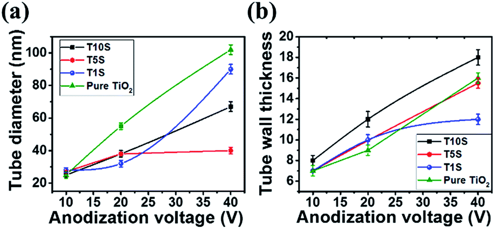 | ||
| Fig. 5 Effect of the anodization voltage on the nanotube diameter (a) and wall thickness (b) formed by the anodic oxidation of the TiSn1 (T1S), TiSn5 (T5S), TiSn10 (T10S) and pure Ti substrates, respectively, for 5 h. | ||
The nanotubes grown on the TiSn10 substrate at 40 V were further analyzed by TEM. Fig. 6(a) displays a bright-field TEM image of the tubular nanotubes in dimensions which are comparable to those in SEM images (S2). The TEM-EDXS shown in Fig. 6(c) was carried out in scanning mode (Fig. 6(b)) and proved that the nanotubes are composed of both Ti and Sn.
 | ||
| Fig. 6 TEM bright-field images of the as-grown nanotubes on the TiSn10 substrate formed at 40 V (a); STEM image of individual nanotubes (b) and the STEM-EDXS analysis confirming that the tubes are composed of Ti and Sn oxides (c). | ||
To provide further information about the chemical composition of the fabricated nanotubes, we conducted X-ray photoelectron spectroscopy (XPS). The obtained XPS survey spectra of the grown nanotubes on the TiSn10 substrate are displayed in Fig. 7. The Ti 2p spectrum (Fig. 7(a)) shows two defined peaks with maxima located at 465 and 459 eV, which are characteristic for the spin–orbit coupling of the Ti 2p1/2 and Ti 2p3/2 orbitals, respectively. The binding energy (BE) position of the peaks confirms the presence of TiO2 and allows us to identify the BE referenced to TiO2.21,35 The Sn 3d spectrum is shown in Fig. 7(b). Two peaks are observed with maxima at 486.8 and 495.2 eV corresponding to the spin–orbit coupling of the Sn 3d5/2 and Sn 3d3/2 orbitals, respectively. The position of the two peaks clearly proves the presence of tin in the oxidation state +IV which is assigned to SnO2.39 Additionally, the existence of metal oxides is indicated by the O 1s spectra (Fig. 7(b)), in which a single peak at 531 eV is observed.14 Representative spectra of carbon with C 1s binding energy in Fig. 7(d) and of fluorine with the F 1s binding energy in Fig. 7(e) show apparent peak maxima located at 284.8 and 684.8 eV, corresponding to carbon and fluorides, respectively.40
 | ||
| Fig. 7 X-ray photoelectron spectra of the grown nanotubes on the TiSn10 substrate at 40 V for the binding energies Ti 2p (a), Sn 3d (b), O 1s (c), C 1s (d) and F 1s (e). | ||
Ethers and alcoholic groups as well as carbonyl groups cannot be excluded as shown by the shoulder at higher binding energies with a local maximum at about 287 eV. The presence of significant amounts of carbon (9.2%) and fluoride (13.6%) species adsorbed on the formed nanotubes is attributed to partial decomposition of the electrolyte as it particularly happens in organic electrolytes during anodization.12 Based on the XPS results, we deduce the successful formation of TiO2/SnO2 nanotube films from the Ti–Sn alloys. The atomic concentrations of Ti and Sn metals of the grown nanotube films were determined at the nanotube surface and after a sputtering time of 8 min corresponding to an abrasion of approximately 28 nm from the oxide surface. The depth-profiling analyses are presented in Table 2. At the nanotube surface, in general the Sn concentrations of all samples show a good representation of the relative alloy concentration and agree well with the EDXS and ICP-OES analyses. The presence of relatively larger amounts of Sn in the formed nanotubes than those in the alloy substrates may be attributed to the etching rate of Sn by anodic oxidation. The etching rate of Sn in the alloy substrates is much higher compared to that of Ti.21 A small decrease in the Sn concentrations was observed after etching T1S and T5S samples. The largest change in the Sn concentration from 11.1 to 6.5 ± 0.1 at% is found for T10S which in accordance with the EDXS mapping results in Fig. 1 indicating the inhomogeneous distribution of Sn metal over the alloy substrate.
| Sample | Measurement condition | Concentration (at%) | |
|---|---|---|---|
| Ti | Sn | ||
| T1S | On surface | 98.3 ± 0.1 | 1.7 ± 0.1 |
| T5S | On surface | 93.6 ± 0.1 | 6.4 ± 0.1 |
| T10S | On surface | 88.9 ± 0.1 | 11.1 ± 0.1 |
| T1S | After sputtering | 98.4 ± 0.1 | 1.6 ± 0.1 |
| T5S | After sputtering | 95.4 ± 0.1 | 4.6 ± 0.1 |
| T10S | After sputtering | 93.5 ± 0.1 | 6.5 ± 0.1 |
To gain further insights into the composition of the present phases, Raman scattering measurements were conducted for the as-fabricated TiO2/SnO2 nanotubes grown at 40 V. As displayed in Fig. 8, six broad signals located at 394, 443, 505, 612, 772 and 891 cm−1 are observed and assigned to amorphous TiO2. These peaks fit very well with the reported spectrum of amorphous TiO2 nanotubes obtained by anodization of a Ti foil.41 The pronounced peaks at about 177 and 579 cm−1 are consistent with the typical Raman spectra of amorphous SnO2 nanomembranes.39 The peak broadening between 400 and 700 cm−1 is attributed to the overlapping Raman modes of TiO2 and SnO2. The Raman spectroscopic analysis also accords with the XRD and XPS results, corroborating the successful formation of TiO2/SnO2 nanotubes.
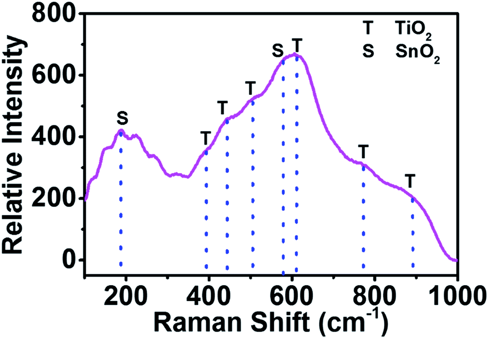 | ||
| Fig. 8 Raman spectrum of the as-formed TiO2/SnO2 grown on the TiSn10 substrate at 40 V. | ||
Electrochemical testing
Cyclic voltammetry tests
The as-formed TiO2 and TiO2/SnO2 nanotubes were directly tested in a cut-off voltage range of 0.1–3 V at a scan rate of 1 mV s−1vs. Li/Li+, since previous studies have shown that amorphous TiO2 exhibits a better performance than crystalline TiO2 because of larger spatial channels created from disorders and defects in amorphous TiO2.42,43 In addition, we observed that the annealing process conducted at 450 °C caused detachment of the nanotube films from the Ti–Sn substrates which may be due to the increased stress on the barrier layer44 (the tube/metal interface). Typical cyclic voltammograms at the second charging/discharging cycle for the as-grown TiO2/SnO2 and the pure TiO2 nanotubes formed at 40 V are shown in Fig. 9. For the TiO2/SnO2 electrode, the CV behaviour in general matches well with previous literature reports.45,46 In the reduction branch of the voltammogram, an apparent peak located at 0.77 V vs. Li/Li+ appears. This peak is typically ascribed to the irreversible decomposition of SnO2 into metallic Sn and the formation of Li2O. Another peak located at 1.25 V vs. Li/Li+ is attributed to the partially reversible conversion reaction of SnO2 into metallic Sn.46 This reaction is also evident in the cathodic branch from the significant sharpness of the main peak at approximately 1.4 V. In addition, a pair of anodic/cathodic peaks is noticed at 0.1 and 0.6 V vs. Li/Li+, respectively, which are associated with the alloying and dealloying reactions to form LixSny compounds.39 For pure TiO2, two main broad peaks in the anodic and cathodic branches are detected in the selected voltage range, as the as-grown nanotubes are amorphous, implying that no phase transition has occurred.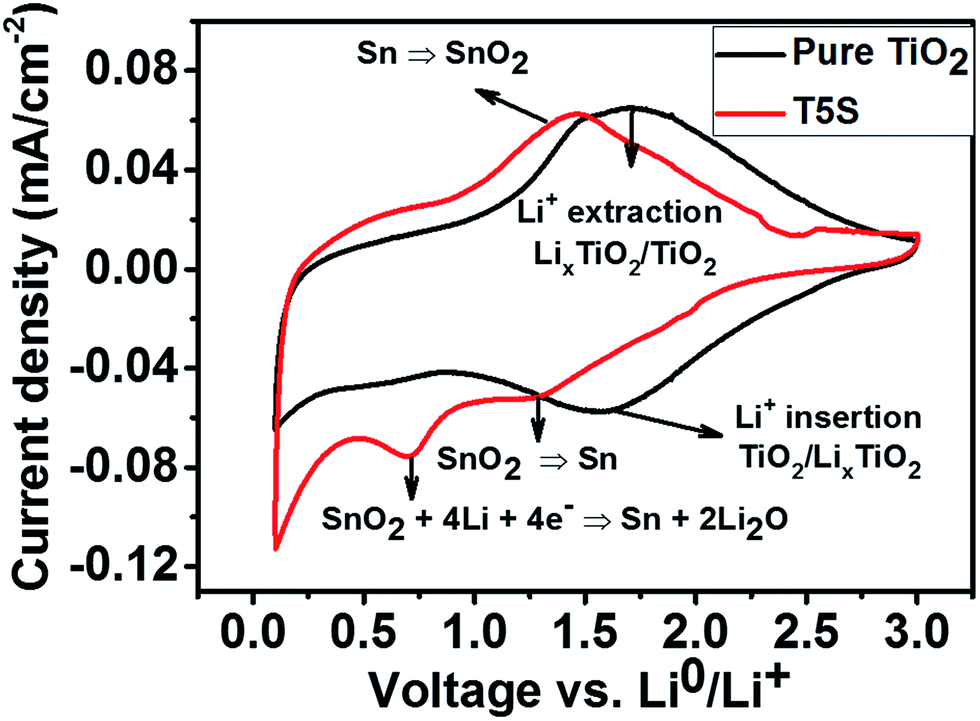 | ||
| Fig. 9 Cyclic voltammograms of TiO2 and TiO2/SnO2 nanotubes (formed on the TiSn5 alloy), prepared at 40 V, and measured at a scan rate of 1 mV s−1. | ||
Galvanostatic cycling
Galvanostatic discharging/charging curves were obtained by cycling the electrodes at a current density of 504 μA cm−2 (i.e. 335 mA g−1) corresponding to a current rate of 1C (1C refers to full charging or discharging in one hour) in Swagelok-type cells between 0.1 and 3 V vs. Li/Li+. Fig. 10(a) shows the voltage profile curves for the first charging (lithium insertion)/discharging (lithium extraction) of the as-formed TiO2 and the TiO2/SnO2 nanotubes. For all electrodes, no well-defined plateaus are noticed in the charging/discharging curves according to the general behaviour of amorphous TiO2-based electrodes and the results are compatible with the CV curves in Fig. 9. The T1S, T5S and T10S electrodes exhibit higher initial discharging/charging capacities, i.e. 2525/1127, 2010/1117 and 1831/1105 μAh cm−2, respectively. We also calculated the gravimetric capacity following the same trend as 1323/590, 1057/585 and 959/579 mA h g−1 corresponding to coulombic efficiencies (CEs) of 44.6, 55.6 and 60.3%, respectively (Fig. 10(b)), compared to pure TiO2 nanotubes with 1272/815 μAh cm−2 (i.e. 666/427 mA h g−1, CE = 64.1%). It is interesting to note that the specific capacities of the electrodes are proportional to the Sn contents of the alloy substrates which relates to the SnO2 mass, suggesting that SnO2 contributes to the whole specific capacity of the electrodes. It is known that SnO2 reacts with Li+ according to a conversion mechanism described by eqn (1) and (2), thus producing a higher theoretical capacity (782 mA h g−1) than pure TiO2 (335 mA h g−1) reacting by an intercalation mechanism. In the lithiation step, SnO2 decomposes into metallic Sn and Li2O resulting in a reduction capacity of 711 mA h g−1 as expressed by eqn (1).39 Afterwards, the reduced Sn undergoes an alloying step in which it reversibly interacts with lithium ions to form LixSn where 0 ≤ x ≤ 4.4 (eqn (2)).47 | ||
| Fig. 10 (a) Typical voltage profiles for the 1st charging/discharging cycle against areal capacity for pure TiO2, T1S, T5S and T10S electrodes, prepared at 40 V anodization voltage, obtained at a current density of 504 μA cm−2. (b) The corresponding coulombic efficiency of the electrodes over 450 charging/discharging cycles. (c) Galvanostatic areal discharging capacities as a function of cycle number obtained at the same current density for pure TiO2 (dark red circles) and TiO2/SnO2 anodes (T1S electrode (green circles), T5S electrode (blue circles) and T10S electrode (black circles)). The mass of each electrode was 1.91 mg cm−2. | ||
Taking into account that the first reaction is partially reversible, the total capacity obtained from both reactions is 782 mA h g−1.
| SnO2 + 4Li+ + 4e− ↔ Sn + 2Li2O | (1) |
| Sn + xLi+ + xe− ↔ LixSn | (2) |
Fig. 10(c) displays the galvanostatic cyclic performance measured at a current density of 504 μA h cm−2 for 420 cycles. All samples show an irreversible discharging/charging capacity in the first cycle assigned to the formation of the solid electrolyte interface (SEI) layer between the electrolyte and the electrode materials. After the first cycle, the specific capacity drops rapidly into a plateau lasting for over 20 cycles. Such rapid capacity fading was reported in previous studies as a common characteristic of amorphous TiO2 and attributed to the increased overpotential during the lithiation/delithiation processes.10 Note that cycling the electrodes in a voltage window below 1 V could be partially another reason for the substantial loss in the specific capacity due to SEI formation at roughly 0.8 V vs. Li/Li+ as a result of electrolyte decomposition which can also explain the low CE values. As presented in the inset of Fig. 10(c), the T1S electrode shows the highest discharging/charging capacity. Compared to pure TiO2, the T1S sample exhibits an average 1.4-fold increase in the specific capacity with excellent cycling stability over 420 cycles. For the T5S electrode, a gradual decrease in the capacity is observed up to about 200 cycles where the specific capacity of pure TiO2 is met. The T10S electrode displays the lowest capacity over around 115 cycles. A significant increase in the specific capacity is then noticed starting from cycle number 50 to number 200 reaching a higher capacity compared to both T5S and pure TiO2 samples. The main reason for the lower capacity of the T10S electrode before 115 cycles could originate from the partially irreversible conversion reaction of SnO2. Due to the partial irreversibility of the conversion reaction, SnO2 becomes inactive upon cycling resulting in a large loss of capacity of the electrode. This behaviour is similar to the cyclic performance of the T5S electrode which contains half the amount of SnO2 compared to T10S. In the case of T1S, the effect of the SnO2 mass on the total electrode mass is small. This fact implies that the presence of such a significant amount of SnO2 in the TiO2/SnO2 electrode may have a positive effect to improve its ionic conductivity, resulting in a higher electrochemical performance. Note that the remarkably better cycling performance is additionally attributed to the high surface area of the T1S sample, exhibiting a thinner tube wall thickness.36 Besides, the thinner tube wall thickness promotes accelerated Li ion diffusion towards the TiO2/SnO2 electrode as a result of the shorter Li ion diffusion path.36,45
In order to further quantify the amount of accessible surface area of the samples, nitrogen physisorption experiments were carried out. The respective isotherms are shown in Fig. 11. All investigated samples show similar sorption isotherms which feature an IUPAC type-III shape. The initial uptake of nitrogen at low relative pressures is rather low, indicating the absence of microporosity. However, at high relative pressures (p/p0 > 0.8) a steep increase in the nitrogen uptake is noticed. Considering the fact that the diameter of the tubes in all samples exceeds 50 nm, a pronounced effect of macroporosity is expected. Thus, the increase of the nitrogen uptake at high relative pressures is attributed to condensation effects. The samples discussed here show a decrease of the specific surface area with increasing Sn content, from 58 m2 g−1 for T1S to 27 m2 g−1 for T10S, as shown in Table 3. These values also correlate with the thickness of the tube walls, which become thicker with increasing amount of Sn. The T1S sample shows the highest specific surface area, for this electrochemical reactions, which in turn leads to a high areal capacity, as shown in Fig. 10(c). The comparatively lower specific surface area of T10S hinders a quick and complete reaction, leading to the lowest areal capacity of all samples already after about 10 cycles.
 | ||
| Fig. 11 Nitrogen physisorption isotherms obtained at 77 K for (a) pure TiO2 (b) T1S (c) T5S and (d) T10S nanotubes prepared at 40 V. | ||
| Sample | Specific surface area (m2 g−1) |
|---|---|
| Pure TiO2 | 47 ± 0.2 |
| T1S | 58 ± 0.2 |
| T5S | 45 ± 0.2 |
| T10S | 27 ± 0.2 |
To investigate the effect of SnO2 on the ionic conductivity of the electrodes, we conducted electrochemical impedance spectroscopy (EIS) measurements for all samples.
The Nyquist plots of pure TiO2 and the TiO2/SnO2 electrodes recorded at 1.7 V vs. Li/Li+ are shown in Fig. 12(a). The spectra are characterized by semicircles at high-to-medium frequencies and inclined lines in the low frequency range. Generally, the semicircles at high-to-medium frequencies represent the charge transfer resistance whilst lithium ions diffuse from the electrolyte across the solid electrode/electrolyte interface.13,36 The inclined lines correspond to solid state diffusion processes of lithium inside the TiO2/SnO2 nanotubes. From these plots, we note that all TiO2/SnO2 electrodes exhibit smaller semicircle diameters than the pure TiO2 electrode. The T10S electrode shows the smallest diameter followed by the T5S and the T1S electrodes indicating a better ionic conductivity with increasing SnO2 content. We suggest that majorly the Li2O originating from the SnO2 decomposition (eqn (1)) is responsible for the enhanced ionic conductivity, similar to that observed for silicon nanostructures.48 The EIS measurements of the T1S electrode were also conducted after 100 charging/discharging cycles at a current density of 504 μA cm−2 and are presented in Fig. 12(d). Only negligible changes in the EIS spectra were observed indicating that the T1S retains its electronic conductivity even after longer cycling times.
 | ||
| Fig. 12 (a) Nyquist plots of pure TiO2 (black circles) and TiO2/SnO2 anodes (T1S electrode (red circles), T5S electrode (blue circles) and T10S electrode (magenta circles)), prepared at 40 V in the frequency range of 100 kHz to 0.1 Hz at a potential of 1.7 V vs. Li/Li+. (b) Rate capability of the T1S, T5S and T10S electrodes formed at 40 V. The filled symbols represent the discharging and open symbols for the charging processes. (c) Morphological characterization of the T1S electrode formed at 40 V after 450 charging/discharging cycles at a current density of 504 μA cm−2. (d) EIS spectra of the T1S electrode before and after 100 cycles at a current density of 504 μAh cm−2. | ||
All electrodes were further tested at different current densities from 50 to 1008 μA cm−2 to demonstrate their rate capability as depicted in Fig. 12(b). Although both electrodes T5S and T10S give higher charge/discharge capacities in comparison with the T1S electrode at a low current density (50 μA cm−2), the capacities decay sharply within the first 10 cycles and finally meet the capacity values of the T1S electrode when the current density increases to 125 μA cm−2. The rapid decrease in the charge/discharge capacities in the first few cycles accords with the general behavior of the T5S and T10S electrodes in the cycling performance presented in Fig. 10(c) which is attributed to the irreversible conversion reaction of SnO2 to nanoparticulate Sn. Both T5S and T10S electrodes display drops in the charging/discharging capacities by increasing the current density stepwise. At the same current rate, the T1S electrode exhibits the highest rate capability with a slower decrease in the charging/discharging capacity. The T1S electrode can deliver average capacities of 780, 660, 490, and 405 μA cm−2 at current densities of 50, 100, 252, 504 and 1008 μA cm−2, respectively. From these results, it is obvious that the T1S electrode exhibits an outstanding reversible rate capability. The electrode can be utilized for practical applications with these high values. To assess the morphological stability, further TEM investigations have been performed for the T1S sample after 450 charging/discharging cycles at a current density of 504 μA cm−2. From the TEM image in Fig. 12(c) it is deduced that the electrode retains its original tubular structure with a marginal deformation of the tube walls.
Conclusions
In the present work, we have demonstrated the electrochemical growth of self-organized mixed titanium and tin oxide nanotubes on the Ti–Sn alloys with different Sn concentrations (1, 5 and 10 at%) as a practicable way to obtain TiO2/SnO2 nanotubes. The as-formed nanotubes are amorphous and their diameters depend on the formation voltage. The characterization results of the oxide films confirmed that the grown nanotubes are comprised of mixed TiO2 and SnO2. The electrochemical tests revealed that the SnO2 contributes to the total capacity of the TiO2/SnO2 electrodes. The TiO2/SnO2 anode grown on the TiSn1 alloy at 40 V displays a 1.4 times increase in the areal capacity compared to pure TiO2 nanotube anodes fabricated and tested under the same conditions over 420 cycles. The enhanced electrochemical performance of TiO2/SnO2 nanotubes is related to the increased lithium ion diffusion resulting from the improved ionic conductivity of TiO2 due to the presence of SnO2 or secondary products. The morphological features of the TiO2/SnO2 nanotubes are well retained upon electrochemical cycling.Acknowledgements
The financial support of the German Federal Ministry of Research and Education is gratefully acknowledged through the project ADNAMSES (grant no. 01DH14002). The authors thank Andrea Voβ for the ICP-OES analysis and Sven Donath for the cold crucible melting of the Ti–Sn alloys.References
- E. C. Evarts, Nature, 2015, 526, S93–S95 CrossRef CAS PubMed.
- Y. Yang, S. Jeong, L. Hu, H. Wu, S. W. Lee and Y. Cui, Proc. Natl. Acad. Sci. U. S. A., 2011, 108, 13013–13018 CrossRef CAS PubMed.
- Y. Qi and S. J. Harris, J. Electrochem. Soc., 2010, 157, A741–A747 CrossRef CAS.
- M. Wagemaker, G. J. Kearley, A. A. Van Well, H. Mutka and F. M. Mulder, J. Am. Chem. Soc., 2003, 125, 840–848 CrossRef CAS PubMed.
- M. Mancini, F. Nobili, R. Tossici, M. Wohlfahrt-Mehrens and R. Marassi, J. Power Sources, 2011, 196, 9665–9671 CrossRef CAS.
- X. Su, Q. Wu, X. Zhan, J. Wu, S. Wei and Z. Guo, J. Mater. Sci., 2012, 47, 2519–2534 CrossRef CAS.
- M. D. Earle, Phys. Rev., 1942, 61, 56–62 CrossRef CAS.
- A. K. Rai, L. T. Anh, J. Gim, V. Mathew, J. Kang, B. J. Paul, J. Song and J. Kim, Electrochim. Acta, 2013, 90, 112–118 CrossRef CAS.
- W. Wen, J. Wu, Y. Jiang, S. Yu, J. Bai, M. Cao and J. Cui, Sci. Rep., 2015, 5, 1–10 Search PubMed.
- W. Wei, G. Oltean, C.-W. Tai, K. Edström, F. Björefors and L. Nyholm, J. Mater. Chem. A, 2013, 1, 8160–8169 CAS.
- H. Hu, L. Yu, X. Gao, Z. Lin and X. W. Lou, Energy Environ. Sci., 2015, 8, 1480–1483 CAS.
- P. Roy, S. Berger and P. Schmuki, Angew. Chem., Int. Ed., 2011, 50, 2904–2939 CrossRef CAS PubMed.
- H. Han, T. Song, E.-K. Lee, A. Devadoss, Y. Jeon, J. Ha, Y.-C. Chung, Y.-M. Choi, Y.-G. Jung and U. Paik, ACS Nano, 2012, 6, 8308–8315 CrossRef CAS PubMed.
- Y. Chen, Y. Tang, S. Luo, C. Liu and Y. Li, J. Alloys Compd., 2013, 578, 242–248 CrossRef CAS.
- P. Zhang, J. Qiu, Z. Zheng, G. Liu, M. Ling, W. Martens, H. Wang, H. Zhao and S. Zhang, Electrochim. Acta, 2013, 104, 41–47 CrossRef CAS.
- Y. Fan, N. Zhang, L. Zhang, H. Shao, J. Wang, J. Zhang and C. Cao, Electrochim. Acta, 2013, 94, 285–293 CrossRef CAS.
- J.-H. Kim, K. Zhu, Y. Yan, C. L. Perkins and A. J. Frank, Nano Lett., 2010, 10, 4099–4104 CrossRef CAS PubMed.
- X. Wu, S. Zhang, L. Wang, Z. Du, H. Fang, Y. Ling and Z. Huang, J. Mater. Chem., 2012, 22, 11151–11185 RSC.
- D. Guan, J. Li, X. Gao and C. Yuan, J. Power Sources, 2014, 246, 305–312 CrossRef CAS.
- L. Yu, Z. Wang, L. Zhang, H. B. Wu and X. W. Lou, J. Mater. Chem. A, 2013, 1, 122–127 CAS.
- M. Madian, L. Giebeler, M. Klose, T. Jaumann, M. Uhlemann, A. Gebert, S. Oswald, N. Ismail, A. Eychmüller and J. Eckert, ACS Sustainable Chem. Eng., 2015, 3, 909–919 CrossRef CAS.
- I. A. Courtney and J. R. Dahn, J. Electrochem. Soc., 1997, 144, 2045–2052 CrossRef CAS.
- J. H. Jeun, K. Y. Park, D. H. Kim, W. S. Kim, H. C. Kim, B. S. Lee, H. Kim, W. R. Yu, K. Kang and S. H. Hong, Nanoscale, 2013, 5, 8480–8483 RSC.
- J. Wang, N. Du, H. Zhang, J. Yu and D. Yang, J. Phys. Chem. C, 2011, 115, 11302–11305 CAS.
- L. Zaraska, N. Czopik, M. Bobruk, G. D. Sulka, J. Mech and M. Jaskuła, Electrochim. Acta, 2013, 104, 549–557 CrossRef CAS.
- M. Radecka, A. Wnuk, A. Trenczek-Zajac, K. Schneider and K. Zakrzewska, Int. J. Hydrogen Energy, 2015, 40, 841–851 CrossRef CAS.
- H. M. Rietveld, J. Appl. Crystallogr., 1969, 2, 65–71 CrossRef CAS.
- T. Roisnel and J. Rodríguez-Carvajal, Mater. Sci. Forum, 2001, 268, 378–381 Search PubMed.
- H. Okamoto, J. Phase Equilib. Diffus., 2010, 31, 202–203 CrossRef CAS.
- I. Szanto, Acta Tech. Acad. Sci. Hung., 1955, 13, 363–372 CAS.
- H. W. Worner, J. Inst. Met., 1953, 81, 521–528 CAS.
- M. Paulose, K. Shankar, S. Yoriya, H. E. Prakasam, O. K. Varghese, G. K. Mor, T. A. Latempa, A. Fitzgerald, C. A. Grimes, U. V. Park and V. Pennsyl, J. Phys. Chem. B, 2006, 110, 16179–16184 CrossRef CAS PubMed.
- G. K. Mor, O. K. Varghese, M. Paulose and C. A. Grimes, Adv. Funct. Mater., 2005, 15, 1291–1296 CrossRef CAS.
- S. P. Albu, D. Kim and P. Schmuki, Angew. Chem., Int. Ed., 2008, 47, 1916–1919 CrossRef CAS PubMed.
- N. K. Allam, A. J. Poncheri and M. A. El-Sayed, ACS Nano, 2011, 5, 5056–5066 CrossRef CAS PubMed.
- Y. Wang, S. Liu, K. Huang, D. Fang and S. Zhuang, J. Solid State Electrochem., 2011, 16, 723–729 CrossRef.
- D. Kim, A. Ghicov and P. Schmuki, Electrochem. Commun., 2008, 10, 1835–1838 CrossRef CAS.
- L. V. Taveira, J. M. Macak, K. Sirotna, L. F. P. Dick and P. Schmuki, J. Electrochem. Soc., 2006, 153, B137–B143 CrossRef CAS.
- X. Liu, J. Zhang, W. Si, L. Xi, S. Oswald, C. Yan and O. G. Schmidt, Nanoscale, 2015, 7, 282–288 RSC.
- S. Sreekantan, K. A. Saharudin, Z. Lockman and T. W. Tzu, Nanotechnology, 2010, 21, 365603 CrossRef PubMed , P1–P8.
- F. Hardcastle, J. Arkansas Acad. Sci., 2011, 65, 43–48 CAS.
- H.-T. Fang, M. Liu, D.-W. Wang, T. Sun, D.-S. Guan, F. Li, J. Zhou, T.-K. Sham and H.-M. Cheng, Nanotechnology, 2009, 20, 22570–1225708 Search PubMed.
- D. Guan, C. Cai and Y. Wang, J. Nanosci. Nanotechnol., 2011, 11, 3641–3650 CrossRef CAS PubMed.
- J. Lin, J. Chen and X. Chen, Electrochem. Commun., 2010, 12, 1062–1065 CrossRef CAS.
- Q. L. Wu, J. Li, R. D. Deshpande, N. Subramanian, S. E. Rankin, F. Yang and Y. Cheng, J. Phys. Chem. C, 2012, 116, 18669–18677 CAS.
- M. Kim, J. Lee, S. Lee, S. Seo, C. Bae and H. Shin, ChemSusChem, 2015, 8, 2363–2371 CrossRef CAS PubMed.
- N. Li and C. R. Martin, J. Electrochem. Soc., 2001, 164–170 CrossRef.
- T. Jaumann, J. Balach, M. Klose, S. Oswald, U. Langklotz, A. Michaelis, J. Eckert and L. Giebeler, Phys. Chem. Chem. Phys., 2015, 17, 24956–24967 RSC.
Footnotes |
| † Electronic supplementary information (ESI) available: The XRD pattern of the as-grown TiO2/SnO2 nanotubes on the TiSn10 alloy. SEM images of the pure TiO2 and TiO2/SnO2 nanotubes. See DOI: 10.1039/c6ta00182c |
| ‡ Present address: Erich Schmid Institute of Materials Science, Austrian Academy of Sciences and Department Materials Physics, Montanuniversität Leoben, Jahnstr. 12, A-8700 Leoben, Austria. |
| This journal is © The Royal Society of Chemistry 2016 |