
 Open Access Article
 This Open Access Article is licensed under a Creative Commons Attribution-Non Commercial 3.0 Unported Licence
Silica-templated ordered mesoporous carbon thin films as electrodes for micro-capacitors†
S.
Leyva-García
a,
D.
Lozano-Castelló
*a,
E.
Morallón
b and
D.
Cazorla-Amorós
a
aDepartamento de Química Inorgánica e Instituto Universitario de Materiales, Universidad de Alicante, E-03080, Alicante, Spain. E-mail: d.lozano@ua
bDepartamento de Química Física e Instituto Universitario de Materiales, Universidad de Alicante, E-03080, Alicante, Spain
First published on 18th February 2016
Abstract
A binderless continuous thin film of a mesoporous carbon material was directly synthesized on a graphite current collector using an ordered mesoporous silica thin film as a hard-template. The nanostructure of the silica, the composite silica/carbon and the mesoporous carbon thin films was characterized by field emission scanning electron microscopy coupled to energy dispersive X-ray spectroscopy, transmission electron microscopy and Raman spectroscopy. The silica thin film, which was uniformly deposited onto the graphite plate surface, presented mesopores of around 8 nm perpendicularly disposed to the current collector. The carbon thin film, which almost replicates the nanostructure of the silica thin film, showed mesopores of around 2–3 nm. Electrochemical characterization of both the mesoporous carbon and the composite silica/carbon thin films, by cyclic voltammetry and galvanostatic charge–discharge in a 1 M H2SO4 solution, demonstrated that the synthesized thin films showed exceptional properties in terms of specific capacitance, rate performance and electrochemical stability to be used as electrodes for micro-capacitors.
Introduction
Supercapacitors (or electrochemical capacitors) are based on the formation of the electric double-layer (EDL) in the interphase electrode–electrolyte and the quick faradic charge transfer reactions between the electrolyte and the electrode (i.e. pseudocapacitance). Porous carbon materials have been intensely investigated as electrodes for supercapacitors because of their low-cost, versatility of structure/texture, good conductivity and high cycling life. Due to these mechanisms in supercapacitors based on carbon electrodes, porous structure and pore size distribution are key parameters to improve the capacitance of the electrodes.1–3 It is well known that micropores provide abundant adsorbing sites for the ions of the electrolyte, thus determining the capacitance values.3–6 Furthermore, the presence of mesopores might be beneficial to interconnect the pore network, thus promoting fast diffusion of the electrolyte.7–11 Accordingly, many studies on the synthesis of microporous, mesoporous and hierarchical ordered carbon materials can be found. Currently, there is an increasing interest on templated carbons because they combine both tailored and ordered porous networks that could result in the development of unique features for energy storage applications.7–10,12–17 Furthermore, in recent times, silica/carbon composites also, which preserve the ordered pore structure of the silica, are being studied as electrodes for electrochemical capacitors.17–19The recent technological trend towards portable electronic devices has led to a strong interest in small-scale energy storage devices. The standard method to prepare carbon electrodes from powdered carbon materials presents some disadvantages e.g. the use of polymeric binders and conductive additives and the high electrical resistivity caused by the presence of macroporosity between the particles. Furthermore, the amount of the active material in the final electrode is between 80 and 90 wt%, which is also a significant drawback. Thin film capacitors (or micro-capacitors) have great potential to be used as power sources in small-scale energy storage devices, because a continuous thin film of a carbon material with the proper porous texture directly synthesized on a suitable current collector could avoid some of the disadvantages associated with the standard preparation method of carbon electrodes. Taking into account that thickness of the electrode plays an important role in the path length for the ions, the thickness of micro-capacitor electrodes (ranging from nm (ref. 20) to few μm (ref. 21)) is a noticeable advantage compared to conventional supercapacitor electrodes (that show thickness from several hundreds of μm (ref. 22)). According to all the aforementioned, micro-capacitors may show high capacitance values and rate performance, which are required for high power density and energy density systems. In this regard, several studies can be found on electrochemical capacitors based on thin films made from: graphene and reduced graphene oxide (rGO),20,23 carbon nanotubes (CNT),24,25 n-doped silicon nanowires26 or conducting polymers e.g. polypyrrole.27 Several works can also be found on interdigitated chips based on transition metal oxides e.g. MnO2 (ref. 28) or RuOx,29 VS2 nanosheets,30 VN and NiO films,31 powdered activated carbon21 or composites containing e.g. rGO,32 graphene33 and carbon fibres34 among others.
Consequently, the objective of the present work is to synthesize a continuous thin film of a mesoporous carbon material directly on a graphite current collector, without the use of binders or conductivity promoters, and to study its potential application as electrodes for micro-capacitors. The carbon thin film was synthesized using an ordered mesoporous silica thin film as a hard template and sucrose as a carbon source. The nanostructure of the silica, the composite silica/carbon and the mesoporous carbon thin films was characterized by field emission scanning electron microscopy (FE-SEM) coupled to energy dispersive X-ray spectroscopy (EDX), transmission electron microscopy (TEM) and Raman spectroscopy. Furthermore, the electrochemical behaviour of mesoporous carbon and composite silica/carbon thin films was analysed in 1 M H2SO4 by cyclic voltammetry (CV) and galvanostatic charge–discharge (GCD) techniques. The results show that both the mesoporous carbon thin film and composite silica/carbon thin film exhibit high specific capacitance and excellent rate performance and electrochemical stability, which make them excellent candidates as electrodes for micro-capacitors.
Experimental
Synthesis of ordered mesoporous silica thin films
To obtain both tailored and ordered mesoporous carbon thin film, a nanostructured silica thin film was successfully synthesized onto the graphite current collector and used as the hard-template. Tetraethoxyorthosilicate (TEOS) was employed as the silica source and the tri-block co-polymer Pluronic®F127 was used as the structure directing agent. A commercial graphite current collector plate (POCO Graphite) of around 15 × 35 mm2 was dip-coated in the precursor solution with the molar ratio of 1 TEOS![[thin space (1/6-em)]](https://www.rsc.org/images/entities/char_2009.gif) :6.60 × 10⁻³ F127:6.66 × 10⁻³ HCl:4.62 H2O:22.6 EtOH (that has been previously used to synthesize a rhombohedral silica thin film by a spin-coating method35). The constant withdrawal rate was 60 mm min−1 and the relative humidity was maintained at 50%. The film was aged at room temperature and relative humidity of 50% during 24 h and, then, it was heated at 80 °C for 24 h. Finally, the synthesized thin film was calcined at 450 °C (ramp of 1 °C min−1) for 5 h in air, in order to eliminate the Pluronic®F127.
:6.60 × 10⁻³ F127:6.66 × 10⁻³ HCl:4.62 H2O:22.6 EtOH (that has been previously used to synthesize a rhombohedral silica thin film by a spin-coating method35). The constant withdrawal rate was 60 mm min−1 and the relative humidity was maintained at 50%. The film was aged at room temperature and relative humidity of 50% during 24 h and, then, it was heated at 80 °C for 24 h. Finally, the synthesized thin film was calcined at 450 °C (ramp of 1 °C min−1) for 5 h in air, in order to eliminate the Pluronic®F127.
Synthesis of mesoporous carbon thin films
A mesoporous carbon thin film was synthesized using sucrose (C12H22O11) as the carbon source and the nanostructured silica thin film as the hard-template. The synthesis is similar to that reported by Ryoo et al.36 Briefly, the synthesized mesoporous silica thin film was dip-coated in an aqueous solution with a molar ratio of 3.65 × 10⁻³ C12H22O11:1.43 × 10⁻³ H2SO4:0.28 H2O. The constant withdrawal rate was 9 mm min−1. The film was then dried at 100 °C for 4 h and, subsequently, pre-carbonized at 160 °C for 4 h. After that, the silica thin film containing partially polymerized and carbonized sucrose was dip-coated in a solution with a molar ratio of 2.34 × 10⁻³ C12H22O11:0.92 × 10⁻³ H2SO4:0.28 H2O. Then, the composite was also dried and pre-carbonized under the same conditions formerly explained. After that, the composite was carbonized in an oven under a N2 flow of 100 ml min−1 at 900 °C (ramp of 10 °C min−1) for 6 h. The mesoporous carbon thin film was obtained by removing the silica template with HF (40%) for 4 h and subsequently washing with copious amounts of deionized water.
SEM, TEM and Raman characterization
FE-SEM (ZEISS, Merlin VP Compact model) coupled to EDX (BRUKER Quantax 400 model) equipment was used to analyse the distribution of the silica thin film onto the graphite plate surface.The nanostructure of the synthesized samples (mesoporous silica, composite silica/carbon and mesoporous carbon thin films) was analysed by TEM (JEOL, JEM-2010 model). A small amount of the sample, obtained by scraping the surface of the graphite plate, was suspended in a few drops of ethanol; and a drop of this suspension was then deposited onto a 300 mesh Lacey copper grid and left to dry at room temperature.
Raman spectroscopy (Jobin-Yvon Horiba LabRam model coupled to an upright microscope Olympus BX30) was employed to further characterize the nanostructure of the composite silica/carbon and mesoporous carbon thin films. Since the spectra obtained from these samples cannot be isolated from the graphite current collector background signal, the Raman spectra of the silica thin film and the bare graphite current corrector were also recorded to better explain the spectra collected from the mesoporous carbon and composite silica/carbon thin films. The excitation line was provided by a 9 mW He–Ne laser at 632.8 nm. The laser beam was focused through a 100× long-working objective. Each spectrum was acquired for 30 s.
Electrochemical characterization
Electrochemical characterization of the mesoporous carbon and the composite silica/carbon thin films was performed in a 1 M H2SO4 solution, using the three-electrode cell configuration. Furthermore, two-electrode cell configuration experiments were performed to study the electrochemical performance of the thin films synthesized in a capacitor. During the electrochemical measurements the temperature was controlled at 25 °C.A typical Pyrex cell for the three-electrode cell configuration test was used. A platinum wire was used as the counter electrode and Ag/AgCl (3.5 M KCl) as the reference electrode. A geometrical area of the synthesized thin film (of 15 × 35 mm2) was immersed in the solution and used as the working electrode.
Two-electrode cells were built using the Swagelok® configuration and gold current collectors, with a Nylon® separator between the thin films. The total geometrical area of the two electrodes used was around 50 mm2.
Regarding the CV characterization, two voltammograms were performed at several scan rates ranging from 2 to 5000 mV s−1. From the 2nd voltammogram the specific capacitance (C in F cm−2) was calculated using eqn (1):
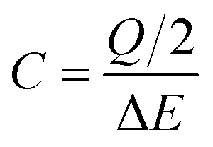 | (1) |
It should be pointed out that, hereafter, cm2 refers to geometrical area of the working electrode in a three-electrode cell configuration and to the sum of the geometrical area of both electrodes in a two-electrode cell configuration.
After the CV characterization GCD was performed at different current densities between 1 and 40 mA cm−2. Additionally, a durability test at 10 mA cm−2 was performed for the two-electrode cell configuration. From the slope of the discharge galvanostatic curve, the specific capacitance (C in F cm−2) was calculated using eqn (2):
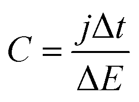 | (2) |
All the electrochemical measurements were performed with potentiostat–galvanostats Biologic (VSP model) and Arbin (SCTS-TA-4 model).
Results and discussion
TEM, SEM and Raman characterization results
Fig. 1a and b show the FE-SEM and the corresponding EDX silicon mapping analysis of the mesoporous silica thin film deposited onto the graphite current collector. Considering that the current collector is commercial graphite synthesized just by pressing graphite particles (randomly oriented in the plate), it presents macropores that are clearly observed in Fig. 1a. From Fig. 1b, it can be seen that the silicon atoms are almost homogeneously distributed, demonstrating that the silica thin film is uniformly deposited onto the graphite current collector. It should be noted that the roughness of the current collector could hinder the registration of the dispersive X-ray signal depending on the orientation of the detector with respect to the surface plate, thus causing dark zones in the image recorded.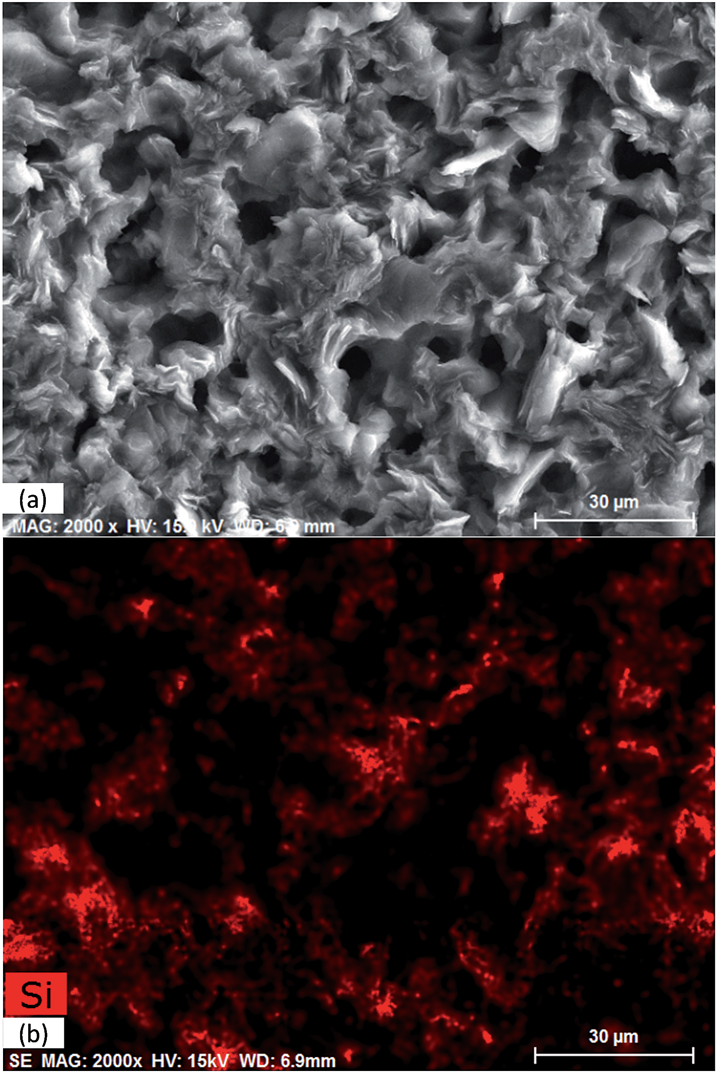 | ||
| Fig. 1 FE-SEM image (a) and corresponding EDX silicon mapping analysis (b) of the mesoporous silica thin film deposited onto the graphite current collector. | ||
TEM images of the silica, the composite silica/carbon and the mesoporous carbon thin films are shown in Fig. 2a–c, respectively. From the TEM image of the silica, it can be seen that the thin film synthesized consists of ordered and homogeneous-size mesopores of around 8 nm, which are perpendicularly disposed to the graphite current collector. The TEM image of the composite silica/carbon thin film shows that the carbon thin film synthesized coats but does not fill the mesopores of the silica. The TEM image of the mesoporous carbon thin film shows that the carbon coating leads to a remarkable decrease of the pore size down to 2–3 nm. This decrease is partially related to the shrinkage of the silica structure due to thermal treatment during the carbonization step.19
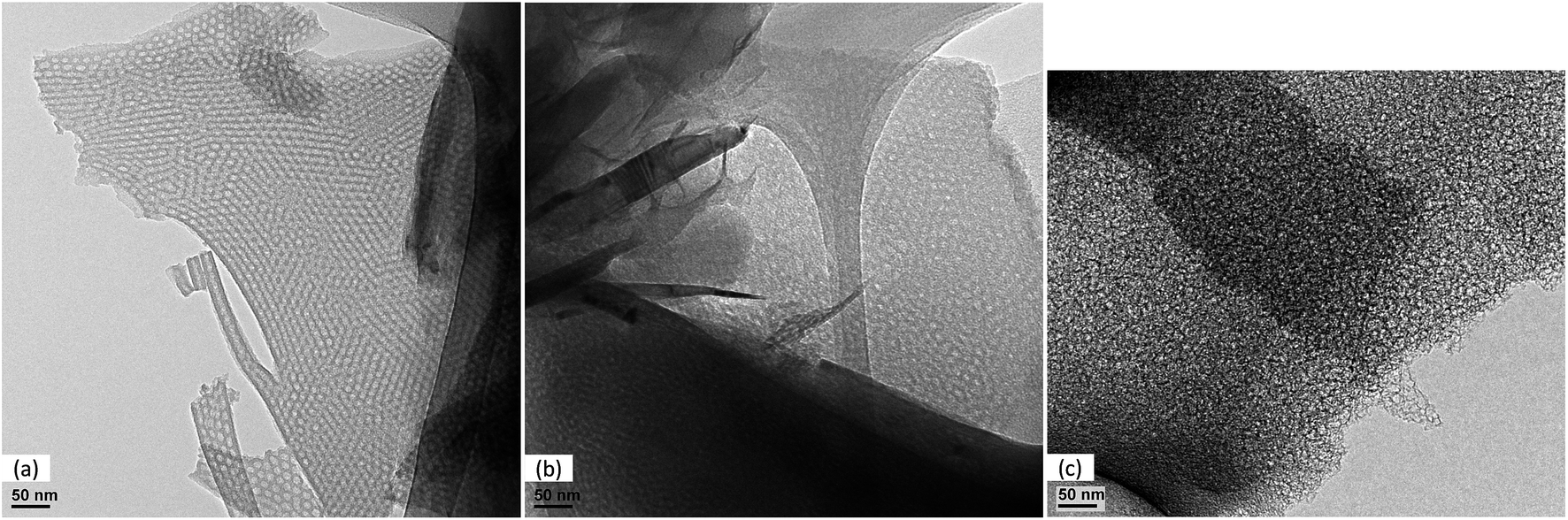 | ||
| Fig. 2 TEM image of: mesoporous silica thin film (a), composite silica/carbon thin film (b) and mesoporous carbon thin film (c). | ||
Furthermore, it seems that by removing the silica template, a partial loss of structural order in the mesoporous carbon thin film occurs.
Several studies found in the literature conclude that the best electrode performance is obtained with porous materials with pores of 2–6 nm,8,18 because mesopores with these sizes improve the kinetics of ion diffusion in the electrode, thus increasing the power performance at large current densities.1 Accordingly, the mesoporous carbon thin film synthesized is expected to show excellent electrochemical behaviour regarding the specific capacitance and retained capacitance values.
Fig. 3 contains the Raman spectra acquired for the bare graphite current collector and the mesoporous silica thin film, the composite silica/carbon and the mesoporous carbon thin films. It should be noted that the thin films were directly analysed on the graphite current collector; therefore, the signal obtained for the samples cannot be isolated from the graphite current collector background signal. All the spectra were normalized versus the D band.
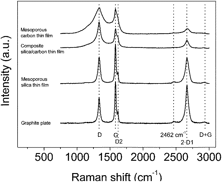 | ||
| Fig. 3 Raman spectra of the graphite plate and the mesoporous silica, composite silica/carbon and mesoporous carbon thin films. Spectra normalized versus the D band. | ||
In general, first- and second-order characteristic bands of carbon materials are observed for all the spectra. Regarding the first-order bands, the G band (1578 cm−1) corresponds to an ideal graphitic lattice vibration mode and the D band (1335 cm−1) is related to the presence of defects.37–41 It should be taken into account that the so-called G and D bands include several bands:38,40–43 the D1 band (that is an inherent mode in the graphite lattice that becomes observable when the symmetry is broken by an edge37,39), the D2 band (1621 cm−1) that has been assigned to a lattice vibration analogous to that of the G band but involving graphene layers which are not directly sandwiched between two other graphene layers (i.e. ‘boundary layer planes’),38,44,45 the D3 band (at around 1500 cm−1) that seems to be related to interstitial defects either between the layers or the basic structural units of carbon films46 or to amorphous carbon47 and the D4 band (at around 1200 cm−1) that has been observed for carbon films with a high content of sp3-carbon45 and it has been assigned to mixed sp2–sp3 bonding.
Concerning the second-order bands (that are attributed to the combination of the first-order bands37,38,41,42,48), the main band appears at 2663 cm−1 which is the first overtone of the D1 band (2·D1). It should be noted that the intensity of the 2·D1 relates to the G band intensity in graphite materials.49 Furthermore, two less intense bands at around 2462 cm−1 and 2937 cm−1, which can be assigned to the first overtone of a Raman inactive graphitic lattice vibration mode at 1220 cm−1 (ref. 37) and to the D + G band, respectively, are also observed.
The Raman spectrum of the bare graphite current collector shows the two typical intense bands of graphite, the first-order G band and the second-order 2·D1 band.50–52 Moreover, the first-order D1 and D2 bands, the D + G second-order band and the one located at 2462 cm−1 are also observed, as previously reported for graphite samples.38,49,53,54
The analysis of the spectra of the thin films synthesized is not straightforward because these signals cannot be isolated from the background graphite plate signal, which, furthermore, may be slightly different depending on the illuminated zone owing to the random orientation of the graphite particles that comprise the graphite plate. The spectrum of the mesoporous silica thin film is almost equal to that from the graphite plate because the signal of the silica is much less intense than that of carbon materials.55,56 From the spectra of the composite silica/carbon and mesoporous carbon thin films, the characteristic G and D bands of carbon materials are observed for the two samples. For the mesoporous carbon thin film, the D and G bands are wider than those from the composite silica/carbon, i.e. it seems that there are higher contributions from the D3 and D4 bands. Therefore, it seems that by removing the silica template the structure of the mesoporous carbon thin film relaxes, thus causing the increase of defects (as previously seen from TEM images, where it was shown that the removal of the silica template produces the partial loss of the mesoporosity order in the carbon thin film). Regarding the different intensities of the 2·D1 band between these two samples, it could be due to the different backgrounds of the graphite plate signal.
Three-electrode cell electrochemical characterization results
Both the mesoporous carbon and composite silica/carbon thin films were characterized by CV and subsequently by GCD experiments. It should be pointed out that the bare graphite was also submitted to the same electrochemical treatment.Prior to electrochemical characterization, the working electrode was subjected to 20 scans between 0.00 V and 0.60 V (where neither oxidation nor reduction took place) at 50 mV s−1 to ensure that the electrode was properly wetted by the electrolyte. Then, the following procedure has been performed on the thin film electrodes. First of all, two voltammograms between 0.00 V and 0.60 V were performed at different scan rates: 2, 5, 10, 20, 50, 100, 200, 500, 1000, 2000 and 5000 mV s−1. Subsequently, two voltammograms at 5 mV s−1 were performed under three subsequent potential ranges going from −0.20 V to 0.80 V, from −0.40 V to 1.00 V and from −0.60 V to 1.00 V. After that, the same electrochemical treatment between 0.00 V and 0.60 V at different scan rates (between 2 and 5000 mV s−1) was applied. Finally, the working electrode was submitted to four charge–discharge cycles between 0.00 and 0.60 V at different current densities: 2, 4, 6, 8, 10, 20 and 40 mA cm−2.
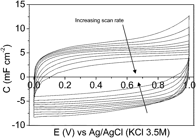
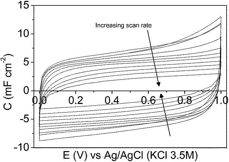
Regarding the CV characterization results, the steady-state 2nd cyclic voltammogram of the experiments is presented. Fig. 4a shows the voltammograms between 0.00 V and 0.60 V for the mesoporous carbon thin film at different scan rates. The voltammograms show a quasi-rectangular shape, typical of an essentially capacitive process associated with the formation of the EDL, even at the high scan rate of 500 mV s−1. It reveals a remarkably low inner resistance compared to conventional electrodes prepared from powdered carbon materials using binders, since even for mesoporous7,15,57 and hierarchical16 powdered carbon materials the shape of the voltammogram got distorted even at lower scan rate values. Fig. 4b shows the voltammograms performed at 5 mV s−1 under different potential windows. The voltammogram performed between −0.20 V and 0.80 V (dash line) shows a quasi-rectangular shape, related to the formation of the EDL; however, during the positive cycle, an anodic current is observed going from 0.60 V to 0.80 V that is presumably related to the oxidation of the electrode material. After broadening the potential window from −0.40 V to 1.00 V (dot line), several redox processes are observed. During the positive sweep a remarkable oxidation current related to the oxidation of the carbon material is recorded going from 0.60 V to 1.00 V, and the corresponding cathodic peak is observed during the subsequent negative cycle at approximately 0.37 V. Furthermore, a cathodic current, presumably related to the electrochemical hydrogen evolution process, is observed from −0.20 V to −0.40 V. Under the potential window between −0.60 V and 1.00 V (solid line) a similar behaviour is observed. But, since the cathodic limit is less positive, higher reduction current associated with the electrochemical hydrogen evolution reaction is observed starting from −0.20 V to more negative potential. The peak related to the oxidation of the adsorbed hydrogen is observed at approximately 0.10 V during the subsequent positive scan.58 In order to analyse the possible modification of the carbon thin film by the previous electrochemical treatment the potential range was changed again to 0.00 V and 0.60 V. Fig. 4c shows the voltammograms performed between 0.00 V and 0.60 V, at different scan rates, after opening the potential window. In this case, the voltammograms also show a quasi-rectangular shape even at high scan rate values. It should be pointed out that the specific capacitance values increase with respect to the voltammograms previously recorded (see Fig. 4a). It seems that, by opening the potential window, the entrance of the ions of the electrolyte in all the pores is promoted, resulting in an increase of the specific capacitance values. Moreover, some pseudocapacitance is observed at low scan rates as a consequence of the formation of oxygen surface groups during the characterization at a high positive potential limit (Fig. 4b).
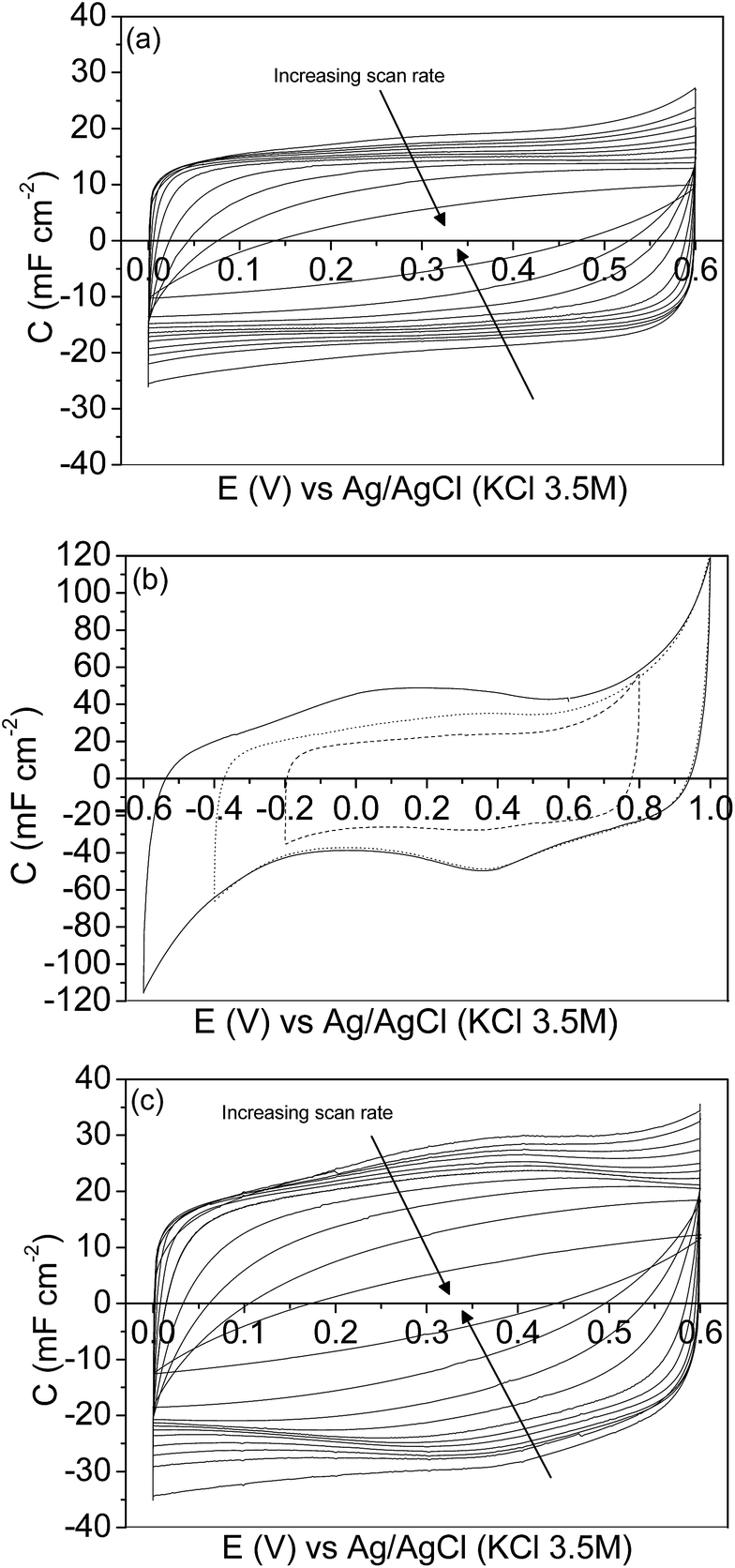 | ||
| Fig. 4 Cyclic voltammograms of the mesoporous carbon thin film in a 1 M H2SO4 solution: between 0.00 V and 0.60 V at 2, 5, 10, 20, 50, 100, 200, 500, 1000, 2000, 5000 mV s−1 (a); between −0.20 and 0.80 V (dash line), between −0.40 V and 1.00 V (dot line) and between −0.60 and 1.00 V (solid line) at 5 mV s−1 (b); between 0.00 V and 0.60 V at 2, 5, 10, 20, 50, 100, 200, 500, 1000, 2000, and 5000 mV s−1 after opening the potential window (c). | ||
Concerning GCD characterization results, the 4th charge–discharge cycle at each current density between 2 and 40 mA cm−2 is shown in Fig. 5. It can be seen that the curves show a quasi-ideal triangular and symmetrical shape, and negligible ohmic drop, typical of a capacitive behaviour associated with the formation of the EDL.
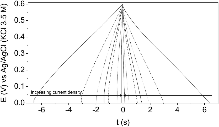 | ||
| Fig. 5 4th charge–discharge cycle of the mesoporous carbon thin film in a 1 M H2SO4 solution at: 2 (solid line), 4 (dash line), 6 (dot line), 8 (solid line), 10 (dash line), 20 (dot line), and 40 (solid line) mA cm−2. | ||
In order to study the behaviour of the mesoporous carbon thin film without removal of the silica template, the same electrochemical treatment was applied to the composite silica/carbon thin film. Since electrochemical charge accommodation during the formation of the EDL takes place exclusively at the surface, the composite silica/carbon thin film is expected to act in a similar way to the mesoporous carbon thin film.
The CV and GCD electrochemical characterization results of the composite silica/carbon thin film are shown in the ESI (see Fig. S1a–c and S2†). From the voltammograms performed between 0.00 V and 0.60 V at different scan rates, both before and after opening the potential window it can be seen that they show a quasi-rectangular shape even at high scan rate values (see Fig. S1a and S1c,† respectively). It should be pointed out that the continuous thin film improves the results reported for powdered carbon-coated mesoporous silica electrodes,17,59 which show a distorted voltammogram shape (i.e. high electrical resistivity) even at low scan rate values.
The specific capacitance values for the mesoporous carbon and the composite silica/carbon thin films at each scan rate and at each current density were calculated from the CV and GCD experiments, respectively.
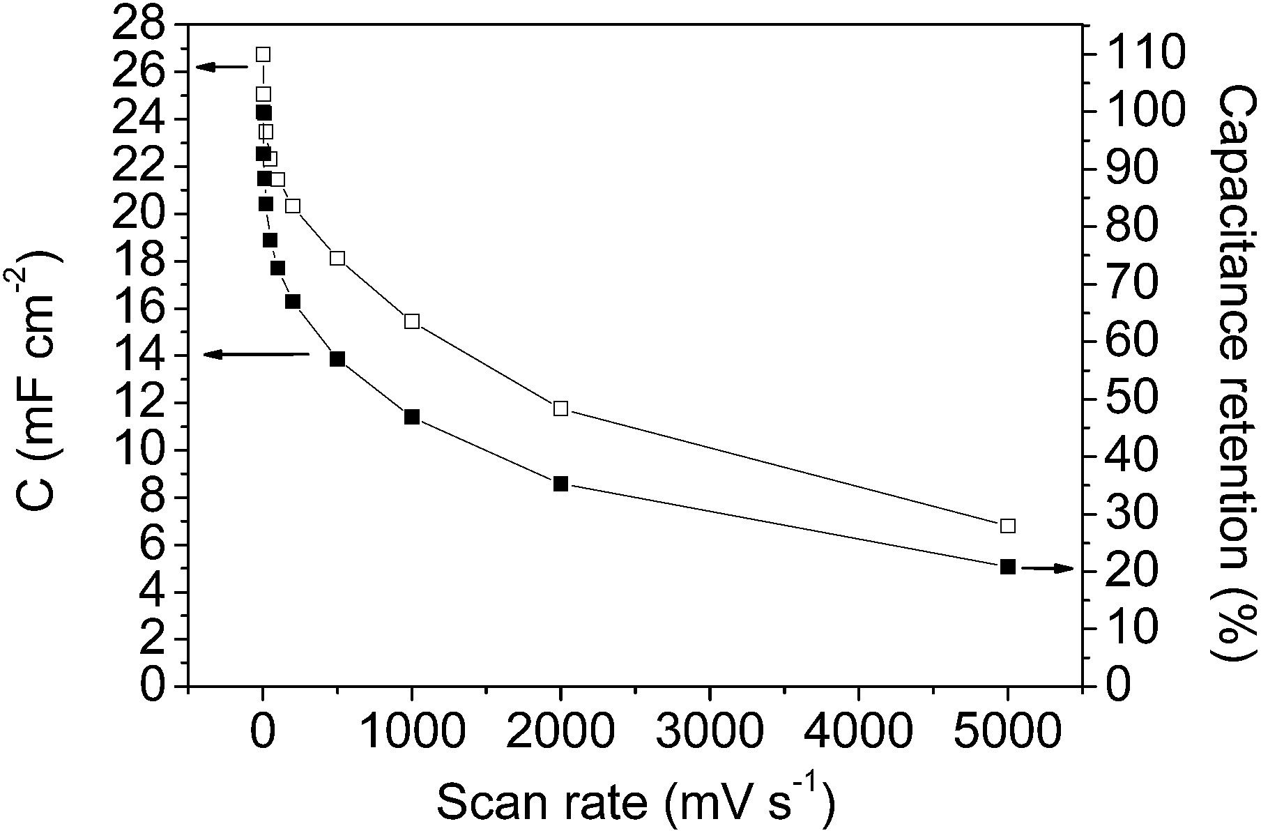
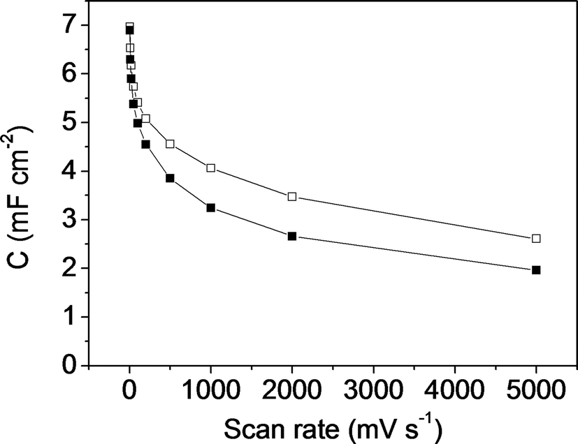
Fig. 6 shows the specific capacitance at each scan rate value calculated before (empty circle symbols) and after (empty square symbols) opening the potential window. In order to show the small contribution of the current collector the specific capacitances for the graphite current collector after opening the potential window (empty triangle symbols) are also included. As has been previously shown from Fig. 4a and c, the capacitance increases after opening the potential window, which is presumably due to the entrance of the electrolyte into all the pores, as a consequence of broadening the potential window, and to the formation of oxygen surface groups that contribute to pseudocapacitance and improve the wetting of the electrolyte. It should be remarked that the very high capacitance value of 26.7 mF cm−2 was recorded at 2 mV s−1 (after opening the potential window).
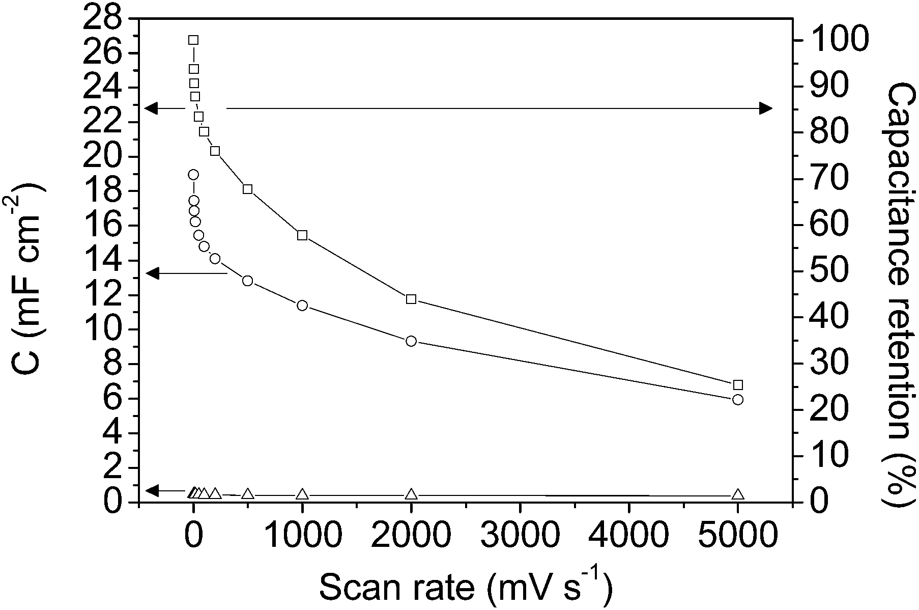 | ||
| Fig. 6 Specific capacitance versus scan rate plot for: graphite current collector after opening the potential window (-Δ- empty triangle symbols) and mesoporous carbon thin film before (-○- empty circle symbols) and after (-□- empty square symbols) opening the potential window. Note: the secondary axis of capacitance retention applies only to the mesoporous carbon thin film after opening the potential window. | ||
It is well known that for materials that combine micro- and mesoporosity high capacitance and rate performance are obtained.11,16 The results obtained, in terms of specific capacitance and capacitance retention, corroborate that the materials synthesized consist of a continuous and ordered thin film with the proper porous texture in which the pathway for the electrolyte shows less tortuosity than that in electrodes made from powdery materials; as a result, the capacitance retention shown is higher than that for electrodes made from powdered hierarchical porous carbon.16 Therefore, the use of a continuous thin film carbon material improves the electrochemical performance of a carbon electrode prepared from a powdered material with regard to its use as an electrode in micro-capacitors.
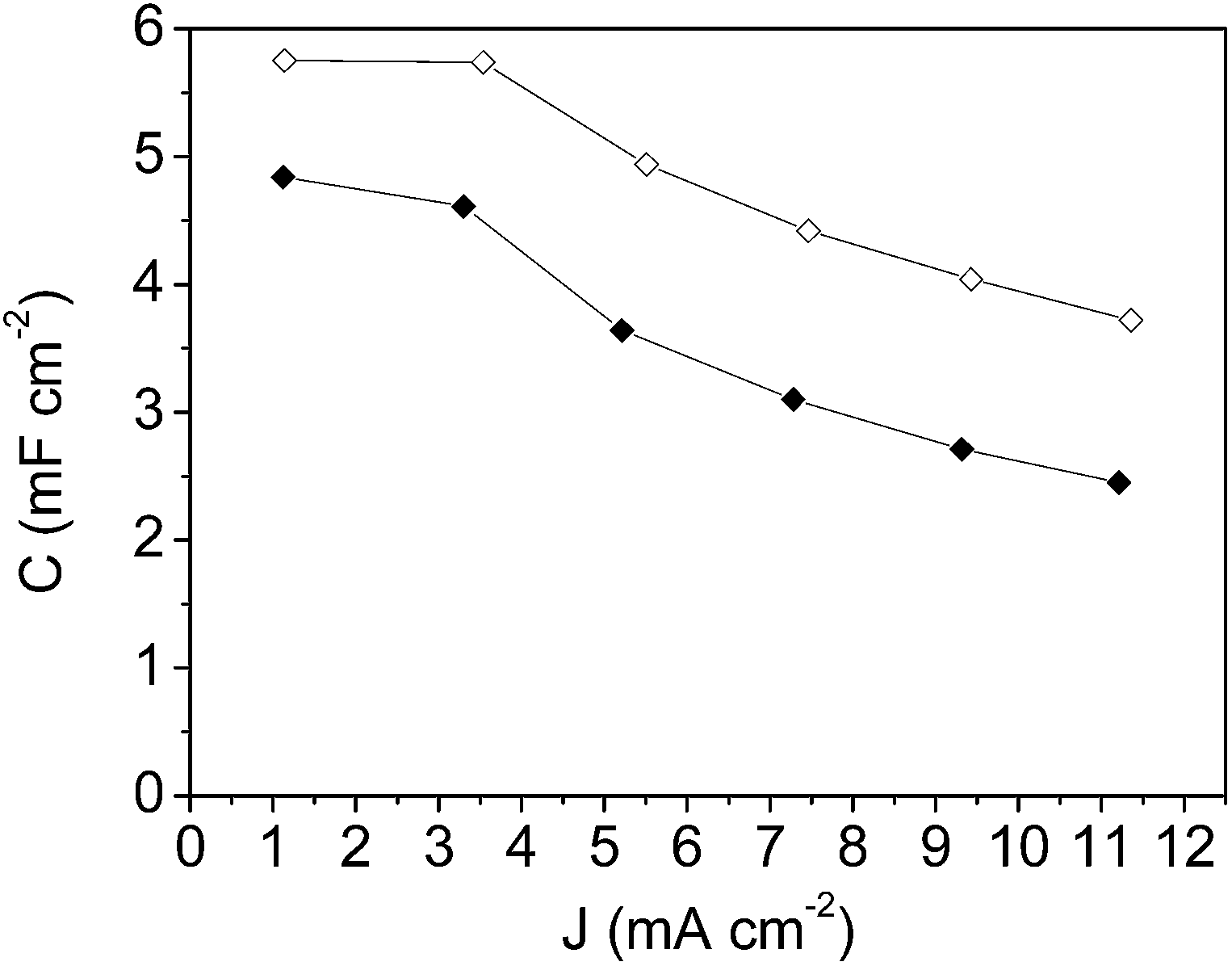
Fig. 7 and 8 show the specific capacitance values versus the scan rate (after opening the potential window) and the current density, respectively, for the mesoporous carbon thin film (empty symbols) and for the composite silica/carbon thin film (full symbols). The results obtained show that the electrochemical behaviour of the composite silica/carbon thin film is similar to that obtained from the mesoporous carbon thin film, confirming that the uniform carbon coating makes the composite possess excellent electrical conductivity. It should be remarked that the very high capacitance value of 24.3 mF cm−2 at 2 mV s−1 was recorded for the composite silica/carbon thin film (see full square symbols in Fig. 7).
 | ||
| Fig. 7 Specific capacitance versus scan rate plot for: mesoporous carbon thin film (-□- empty square symbols) and composite silica/carbon thin film (-■- full square symbols) after opening the potential window. Note: the secondary axis of capacitance retention applies only to the composite silica/carbon thin film. | ||
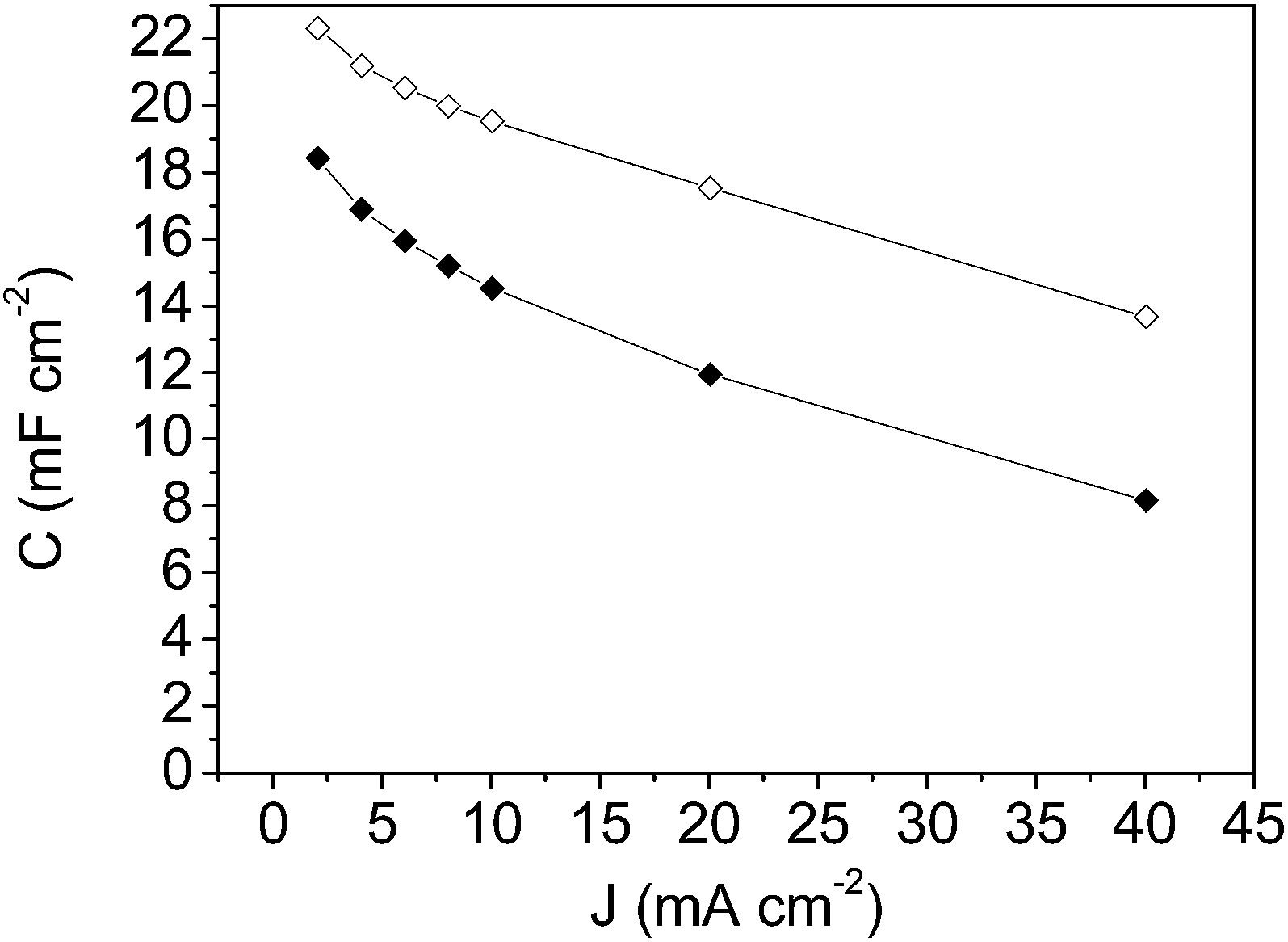 | ||
| Fig. 8 Specific capacitance versus current density plot for: mesoporous carbon thin film (-◊- empty rhombus symbols) and composite silica/carbon thin film (-◆- full rhombus symbols). | ||
From the results shown in Fig. 8, it should be pointed out that the high specific capacitance value of 22.3 mF cm−2 at 2 mA cm−2 for the mesoporous carbon thin film and the high capacitance retention (61%) at the highest current density of 40 mA cm−2 were achieved. These high specific capacitance values are in the same order of magnitude as that obtained for a zeolite-templated carbon thin film.60 From the results for the composite silica/carbon thin film it should be pointed out that at 2 mA cm−2 the capacitance is 18.4 mF cm−2, and at the highest current density of 40 mA cm−2 the electrode even retains 44% of the initial capacitance (giving a capacitance of 8.2 mF cm−2) (see full rhombus symbols).
The electrochemical characterization results show the exceptional electrochemical properties of the mesoporous carbon thin film and that it may be a suitable candidate as electrodes for micro-capacitors. Furthermore, it has been shown that the formation of a uniform carbon coating over the silica template makes the composite have an excellent electrical conductivity despite the insulating nature of the silica.17–19,59,61 Therefore, the composite silica/carbon thin film exhibits excellent electrical conductivity and electrochemical behaviour to be directly used as electrodes for micro-capacitors, which is very interesting from economical and environmental points of view.
Two-electrode cell electrochemical characterization results
It has been shown that both the mesoporous carbon and composite silica/carbon thin films show exceptional electrochemical properties to be used as electrodes for electrochemical micro-capacitors. Therefore, the thin films synthesized were characterized in a symmetric two-electrode cell. The symmetric electrochemical capacitor was characterized by CV and subsequently by GCD. After that, the capacitor was submitted to a durability test.Regarding the CV characterization, two voltammograms between 0.00 V and 1.00 V were performed at different scan rates: 5, 10, 20, 50, 100, 200, 500, 1000, 2000 and 5000 mV s−1.
Subsequently, the GCD characterization was accomplished by performing four charge–discharge cycles between 0.00 and 1.00 V at different current densities: 1, 3, 5, 7, 9 and 11 mA cm−2 (it should be reminded that for the two-electrode electrochemical characterization cm−2 refers to the sum of the geometrical area of both the positive and negative electrodes). Finally, a durability test was carried out, consisting of 25000 GCD cycles under two subsequent potential ranges (from 0.00 V to 1.00 V and from 0.00 V to 1.20 V).
Fig. 9 and 10 show the steady-state 2nd cyclic voltammogram at each potential range for the symmetric electrochemical capacitor made from the mesoporous carbon and the composite silica/carbon thin films, respectively. The voltammograms show a quasi-rectangular shape even at high scan rate values, thus improving the electrochemical behaviour of conventional electrochemical capacitors made from powdered carbon materials using binders62,63 or micro-devices based on carbon fibres,34 where the shape of the voltammogram gets distorted even at lower scan rate values.
 | ||
| Fig. 9 Cyclic voltammograms of the symmetric electrochemical capacitor from the mesoporous carbon thin film in a 1 M H2SO4 solution between 0.00 V and 1.00 V at: 5, 10, 20, 50, 100, 200, 500, 1000, 2000, and 5000 mV s−1. | ||
 | ||
| Fig. 10 Cyclic voltammograms of the symmetric electrochemical capacitor from the composite silica/carbon thin film in a 1 M H2SO4 solution between 0.00 V and 1.00 V at: 5, 10, 20, 50, 100, 200, 500, 1000, 2000, and 5000 mV s−1. | ||
Fig. 11 shows the specific capacitance versus the scan rate for the symmetric electrochemical capacitor made from the mesoporous carbon thin film (empty square symbols) and from the composite silica/carbon thin film (full square symbols). Analogously, in Fig. 12, the specific capacitance is presented versus the current density (calculated from the GCD, not shown here) for the mesoporous carbon thin film (empty rhombus symbols) and from the composite silica/carbon thin film (full rhombus symbols) symmetric capacitors. In general, the results obtained show similar electrochemical behaviour for both the mesoporous carbon and the composite silica/carbon thin film symmetric electrochemical capacitor, as previously seen from the three-electrode cell configuration characterization results.
 | ||
| Fig. 11 Specific capacitance versus scan rate plot for the symmetric electrochemical capacitor made from: the mesoporous carbon thin film (-□- empty square symbols) and the composite silica/carbon thin film (-■- full square symbols). | ||
 | ||
| Fig. 12 Specific capacitance versus current density plot for the symmetric electrochemical capacitor made from: the mesoporous carbon thin film (-◊- empty rhombus symbols) and the composite silica/carbon thin film (-◆- full rhombus symbols). | ||
It should be remarked that the very high capacitance values of 7.0 mF cm−2 and 6.9 mF cm−2 were recorded at 5 mV s−1 for the mesoporous carbon and the composite silica/carbon thin film symmetric capacitors, respectively (Fig. 11). Even though the comparison is not straightforward (because of the different experimental assembly and electrochemical conditions), the results obtained improve the value reported for an interdigitated micro-capacitor based on powdered activated carbon (2.1 mF cm−2).21 By increasing the scan rate up to 5000 mV s−1 the capacitance retention values of the electrochemical capacitor are 37% and 28% for the mesoporous carbon and the composite silica/carbon thin film electrodes, respectively, which is a remarkable result considering that the microelectrode assembly is not the most adequate one. Even then, the specific capacitance values are comparable to those found in the literature for interdigitated micro-capacitors based on reduced graphene oxide or graphene composites32,33 and onion-like carbon,64 and for micro-capacitors made of rGO thin films.20
From Fig. 12, it should be remarked that the high specific capacitance values were obtained at low current densities (1 and 3 mA cm−2), of around 5.7 mF cm−2 and 4.7 mF cm−2 for the mesoporous carbon thin film and the composite silica/carbon thin film symmetric electrochemical capacitor, respectively, which are similar to those obtained for micro-capacitors based on rGO–CNT composites.32
Fig. 13 shows the durability test results for the mesoporous carbon thin film symmetric electrochemical capacitor. This figure includes the first 25000 cycles performed between 0.00 V and 1.00 V and the 25000 cycles subsequently performed between 0.00 V and 1.20 V. A slight decrease can be seen in the specific capacitance even after the high number of cycles performed (more pronounced in the first 25000 cycles), which indicates a very low degradation of the mesoporous carbon thin film electrodes. A very similar behaviour, i.e., low decrease of the specific capacitance value even after very high number of cycles was observed for the durability test done for the composite silica/carbon thin film (results not shown here). Even though straightforward comparison is not fair, these results point out the superior durability of capacitors made from the thin films synthesized compared to conventional electrochemical capacitors made from powdered carbon materials that are not usually subjected to such a high number of galvanostatic charge–discharge cycles and also they show a decrease of the capacitance retention even after less number of cycles applied.65–67
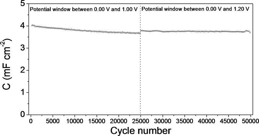 | ||
| Fig. 13 Specific capacitance versus cycle number plot for the symmetric electrochemical capacitor made from the mesoporous carbon thin film: between 0.00 V and 1.00 V and between 0.00 V and 1.20 V. | ||
Thus, both the mesoporous carbon thin film and the composite silica/carbon thin film show exceptional electrochemical properties, in terms of capacitance, rate performance and stability, making them promising candidates as electrodes for micro-capacitors.
Conclusions
A continuous mesoporous carbon thin film was successfully synthesized onto a graphite current collector using an ordered mesoporous silica thin film as the hard-template. The nanostructure of the silica, the composite silica/carbon and the mesoporous carbon thin films was characterized by microscopy and spectroscopy techniques. FE-SEM and corresponding EDX silicon mapping analysis of the mesoporous silica thin film demonstrated that it is uniformly deposited onto the graphite current collector. From TEM images it is shown that the silica template presents ordered mesopores of around 8 nm perpendicularly disposed to the graphite current collector. From the image of the composite silica/carbon thin film it is shown that the carbon material covers the nanostructure of the template and it maintains the structural order of the silica thin film. A TEM image of the mesoporous carbon thin film demonstrated that the order partially decreases by removing the silica template and that the mesopore size is around 2–3 nm. A mesoporous carbon thin film Raman spectrum shows an increment of the D and G band width with respect to the composite silica/carbon thin film spectrum, pointing out that the removal of the silica template produces a relaxation of the mesoporous carbon thin film structure: the structural order of the carbon materials decreases that entails the appearance of defects. This result is in agreement with the partial loss of the mesoporosity order previously observed from TEM images. Concerning the electrochemical characterization, it should be pointed out that the very high capacitance values of 7.0 mF cm−2 and 6.9 mF cm−2 were recorded at 5 mV s−1 for the mesoporous carbon and the composite silica/carbon thin film symmetric capacitors, respectively, that improve the values reported for other carbon-based electrode devices. The very similar electrochemical results (high specific capacitance and high rate performance) obtained for both thin films (mesoporous carbon and silica/carbon composite) demonstrate that the uniform carbon coating makes the composite possess excellent electrical conductivity. Furthermore, the durability test has shown that the thin films synthesized show low degradation, even after a high number of cycles are applied, since the specific capacitance remains almost constant. Therefore, both the mesoporous carbon thin film and the composite silica/carbon thin film show exceptional electrochemical properties, in terms of capacitance, rate performance and stability, making them promising candidates as electrodes for micro-capacitors.Acknowledgements
The authors would like to thank the MINECO (MAT2013-42007-P and CTQ2012/31762) and GV and FEDER (PROMETEOII/2014/010). SLG thanks Spanish MECD for the thesis grant.Notes and references
- L. L. Zhang, Z. Lei, J. Zhang, X. Tian and X. S. Zhao, in Supercapacitors: Electrode Materials Aspects, ed. R. H. Crabtree, John Wiley & Sons, New Haven, 2010, p. 341 Search PubMed.
- F. Béguin, E. Raymundo-Piñero and E. Frackowiak, in Electrical Double-Layer Capacitors and Pseudocapacitors, ed. F. Béguin and E. Frackowiak, CRC Press, Pennsylvania, 2010, p. 329 Search PubMed.
- M. J. Bleda-Martinez, D. Lozano-Castello, D. Cazorla-Amoros and E. Morallon, Energy Fuels, 2010, 24, 3378–3384 CrossRef CAS.
- M. Liu, J. Qian, Y. Zhao, D. Zhu, L. Gan and L. Chen, J. Mater. Chem. A, 2015, 3, 11517–11526 CAS.
- Y. Zhao, M. Liu, X. Deng, L. Miao, P. K. Tripathi, X. Ma, D. Zhu, Z. Xu, Z. Hao and L. Gan, Electrochim. Acta, 2015, 153, 448–455 CrossRef CAS.
- Y. Zhao, M. Liu, L. Gan, X. Ma, D. Zhu, Z. Xu and L. Chen, Energy Fuels, 2014, 28, 1561–1568 CrossRef CAS.
- H. Liu, K. Wang and H. Teng, Carbon, 2005, 43, 559–566 CrossRef CAS.
- A. Fuertes, G. Lota, T. Centeno and E. Frackowiak, Electrochim. Acta, 2005, 50, 2799–2805 CrossRef CAS.
- K. Kim, M. Choi and R. Ryoo, Carbon, 2013, 60, 175–185 CrossRef CAS.
- S. Yoon, J. Lee, T. Hyeon and S. M. Oh, J. Electrochem. Soc., 2000, 147, 2507–2512 CrossRef CAS.
- R. Ruiz-Rosas, M. J. Valero-Romero, D. Salinas-Torres, J. Rodriguez-Mirasol, T. Cordero, E. Morallon and D. Cazorla-Amoros, ChemSusChem, 2014, 7, 1458–1467 CrossRef CAS PubMed.
- D. W. Wang, F. Li, H. T. Fang, M. Liu, G. Q. Lu and H. M. Cheng, J. Phys. Chem. B, 2006, 110, 8570–8575 CrossRef CAS PubMed.
- A. Fuertes, F. Pico and J. Rojo, J. Power Sources, 2004, 133, 329–336 CrossRef CAS.
- H. Nishihara and T. Kyotani, Adv. Mater., 2012, 24, 4473–4498 CrossRef CAS PubMed.
- H. Zhou, S. Zhu, M. Hibino and I. Honma, J. Power Sources, 2003, 122, 219–223 CrossRef CAS.
- K. Xia, Q. Gao, J. Jiang and J. Hu, Carbon, 2008, 46, 1718–1726 CrossRef CAS.
- T. Kwon, H. Nishihara, Y. Fukura, K. Inde, N. Setoyama, Y. Fukushima and T. Kyotani, Microporous Mesoporous Mater., 2010, 132, 421–427 CrossRef CAS.
- J. Zhi, Y. Wang, S. Deng and A. Hu, RSC Adv., 2014, 4, 40296–40300 RSC.
- S. M. Filonenko, N. D. Shcherban, P. S. Yaremov and V. S. Dyadyun, J. Porous Mater., 2015, 22, 21–28 CrossRef CAS.
- J. J. Yoo, K. Balakrishnan, J. Huang, V. Meunier, B. G. Sumpter, A. Srivastava, M. Conway, A. L. M. Reddy, J. Yu, R. Vajtai and P. M. Ajayan, Nano Lett., 2011, 11, 1423–1427 CrossRef CAS PubMed.
- D. Pech, M. Brunet, P. Taberna, P. Simon, N. Fabre, F. Mesnilgrente, V. Conedera and H. Durou, J. Power Sources, 2010, 195, 1266–1269 CrossRef CAS.
- F. Beguin, V. Presser, A. Balducci and E. Frackowiak, Adv. Mater., 2014, 26, 2219–2251 CrossRef CAS PubMed.
- L. Oakes, A. Westover, J. W. Mares, S. Chatterjee, W. R. Erwin, R. Bardhan, S. M. Weiss and C. L. Pint, Sci. Rep., 2013, 3, 1–7 Search PubMed.
- J. Kim, K. Nam, S. Ma and K. Kim, Carbon, 2006, 44, 1963–1968 CrossRef CAS.
- M. Kaempgen, C. K. Chan, J. Ma, Y. Cui and G. Gruner, Nano Lett., 2009, 9, 1872–1876 CrossRef CAS PubMed.
- F. Thissandier, N. Pauc, T. Brousse, P. Gentile and S. Sadki, Nanoscale Res. Lett., 2013, 8, 1–5 CrossRef PubMed.
- W. Sun, R. Zheng and X. Chen, J. Power Sources, 2010, 195, 7120–7125 CrossRef CAS.
- I. Nam, G. Kim, S. Park, J. Park, N. D. Kim and J. Yi, Nanoscale, 2012, 4, 7350–7353 RSC.
- S. Makino, Y. Yamauchi and W. Sugimoto, J. Power Sources, 2013, 227, 153–160 CrossRef CAS.
- J. Feng, X. Sun, C. Wu, L. Peng, C. Lin, S. Hu, J. Yang and Y. Xie, J. Am. Chem. Soc., 2011, 133, 17832–17838 CrossRef CAS PubMed.
- E. Eustache, R. Frappier, R. L. Porto, S. Bouhtiyya, J. Pierson and T. Brousse, Electrochem. Commun., 2013, 28, 104–106 CrossRef CAS.
- M. Beidaghi and C. Wang, Adv. Funct. Mater., 2012, 22, 4501–4510 CrossRef CAS.
- Y. S. Moon, D. Kim, G. Lee, S. Y. Hong, K. K. Kim, S. M. Park and J. S. Ha, Carbon, 2015, 81, 29–37 CrossRef CAS.
- W. Liu, N. Liu, Y. Shi, Y. Chen, C. Yang, J. Tao, S. Wang, Y. Wang, J. Su, L. Li and Y. Gao, J. Mater. Chem. A, 2015, 3, 13461–13467 CAS.
- H. Lee, J. Yang, H. Lee, J. Park, K. Lee and Y. Kwon, J. Mater. Chem., 2008, 18, 1881–1888 RSC.
- R. Ryoo, S. Joo and S. Jun, J. Phys. Chem. B, 1999, 103, 7743–7746 CrossRef CAS.
- Y. Wang, D. C. Alsmeyer and R. L. McCreery, Chem. Mater., 1990, 2, 557–563 CrossRef CAS.
- A. Sadezky, H. Muckenhuber, H. Grothe, R. Niessner and U. Poschl, Carbon, 2005, 43, 1731–1742 CrossRef CAS.
- F. Tuinstra and J. L. Koenig, J. Chem. Phys., 1970, 53, 1126–1130 CrossRef CAS.
- T. Jawhari, A. Roid and J. Casado, Carbon, 1995, 33, 1561–1565 CrossRef CAS.
- E. F. Antunes, A. O. Lobo, E. J. Corat, V. J. Trava-Airoldi, A. A. Martin and C. Veríssimo, Carbon, 2006, 44, 2202–2211 CrossRef CAS.
- A. Cuesta, P. Dhamelincourt, J. Laureyns, A. Martínez-Alonso and J. Tascón, Carbon, 1994, 32, 1523–1532 CrossRef CAS.
- S. Sze, N. Siddique, J. Sloan and R. Escribano, Atmos. Environ., 2001, 35, 561–568 CrossRef CAS.
- R. J. Bowling, R. T. Packard and R. L. McCreery, J. Am. Chem. Soc., 1989, 111, 1217–1223 CrossRef CAS.
- J. Schwan, S. Ulrich, V. Batori, H. Ehrhardt and S. Silva, J. Appl. Phys., 1996, 80, 440–447 CrossRef CAS.
- J. N. Rouzaud, A. Oberlin and C. Beny-Bassez, Thin Solid Films, 1983, 105, 75–96 CrossRef CAS.
- N. P. Ivleva, A. Messerer, X. Yang, R. Niessner and U. Poeschl, Environ. Sci. Technol., 2007, 41, 3702–3707 CrossRef CAS PubMed.
- A. Sood, R. Gupta and S. Asher, J. Appl. Phys., 2001, 90, 4494–4497 CrossRef CAS.
- E. del Corro, M. Taravillo and V. G. Baonza, J. Raman Spectrosc., 2014, 45, 476–480 CrossRef.
- R. Krishna, A. N. Jones, R. Edge and B. J. Marsden, Radiat. Phys. Chem., 2015, 111, 14–23 CrossRef CAS.
- A. C. Ferrari, Solid State Commun., 2007, 143, 47–57 CrossRef CAS.
- A. C. Ferrari, J. C. Meyer, V. Scardaci, C. Casiraghi, M. Lazzeri, F. Mauri, S. Piscanec, D. Jiang, K. S. Novoselov, S. Roth and A. K. Geim, Phys. Rev. Lett., 2006, 97, 187401 CrossRef CAS PubMed.
- R. Krishna, A. N. Jones and B. J. Marsden, Radiat. Phys. Chem., 2015, 107, 121–127 CrossRef CAS.
- Y. Kawashima and G. Katagiri, Phys. Rev. B: Condens. Matter Mater. Phys., 1999, 59, 62–64 CrossRef CAS.
- M. Laskowska, Ł. Laskowski and K. Dzilinski, Curr. Top. Biophys., 2012, 35, 11–18 CAS.
- D. Carboni, B. Lasio, V. Alzari, A. Mariani, D. Loche, M. F. Casula, L. Malfatti and P. Innocenzi, Phys. Chem. Chem. Phys., 2014, 16, 25809–25818 RSC.
- G. Q. Lu, Z. F. Yan, W. Xing, S. Z. Qiao, R. G. Ding, F. Li and H. M. Cheng, Carbon, 2006, 44, 216–224 CrossRef.
- K. Jurewicz, E. Frackowiak and F. Beguin, Appl. Phys. A, 2004, 78, 981–987 CrossRef CAS.
- H. Nishihara, T. Kwon, Y. Fukura, W. Nakayama, Y. Hoshikawa, S. Iwamura, N. Nishiyama, T. Itoh and T. Kyotani, Chem. Mater., 2011, 23, 3144–3151 CrossRef CAS.
- A. Berenguer-Murcia, R. R. Ruiz-Rosas, J. Garcia-Aguilar, K. Nueangnoraj, H. Nishihara, E. Morallon, T. Kyotani and D. Cazorla-Amoros, Phys. Chem. Chem. Phys., 2013, 15, 10331–10334 RSC.
- H. Nishihara, Y. Fukuraa, K. Inde, K. Tsuji, M. Takeuchi and T. Kyotani, Carbon, 2008, 46, 48–53 CrossRef CAS.
- Y. Gao, L. Li, Y. Jin, Y. Wang, C. Yuan, Y. Wei, G. Chen, J. Ge and H. Lu, Appl. Energy, 2015, 153, 41–47 CrossRef CAS.
- E. J. Lee, Y. J. Lee, J. K. Kim, M. Lee, J. Yi, J. R. Yoon, J. C. Song and I. K. Song, Mater. Res. Bull., 2015, 70, 209–214 CrossRef CAS.
- D. Pech, M. Brunet, H. Durou, P. Huang, V. Mochalin, Y. Gogotsi, P. Taberna and P. Simon, Nat. Nanotechnol., 2010, 5, 651–654 CrossRef CAS PubMed.
- I. I. G. Inal, S. M. Holmes, A. Banford and Z. Aktas, Appl. Surf. Sci., 2015, 357, 696–703 CrossRef CAS.
- V. Khomenko, E. Raymundo-Pinero, E. Frackowiak and F. Beguin, Appl. Phys. A: Mater. Sci. Process., 2006, 82, 567–573 CrossRef CAS.
- G. Huang, W. Kang, B. Xing, L. Chen and C. Zhang, Fuel Process. Technol., 2016, 142, 1–5 CrossRef CAS.
Footnote |
| † Electronic supplementary information (ESI) available. See DOI: 10.1039/c5ta10552h |
| This journal is © The Royal Society of Chemistry 2016 |