
 Open Access Article
 This Open Access Article is licensed under a Creative Commons Attribution-Non Commercial 3.0 Unported Licence
Efficient bifacial dye-sensitized solar cells through disorder by design†
José M.
Miranda-Muñoz
,
Sol
Carretero-Palacios
,
Alberto
Jiménez-Solano
,
Yuelong
Li
,
Gabriel
Lozano
and
Hernán
Míguez
*
Multifunctional Optical Materials Group, Institute of Materials Science of Sevilla, Consejo Superior de Investigaciones Científicas – Universidad de Sevilla (CSIC-US), Américo Vespucio 49, 41092, Sevilla, Spain. E-mail: h.miguez@csic.es
First published on 14th January 2016
Abstract
Herein we realize an optical design that optimizes the performance of bifacial solar cells without modifying any of the usually employed components. In order to do so, dielectric scatterers of controlled size and shape have been successfully integrated in the working electrodes of dye-sensitized solar cells (DSSCs), resulting in bifacial devices of outstanding performance. Power conversion efficiencies (PCEs) as high as 6.7% and 5.4% have been attained under front and rear illumination, respectively, which represent a 25% and a 33% PCE enhancement with respect to an 8 μm-thick standard solar cell electrode using platinum as the catalytic material. The remarkable bifacial character of our approach is demonstrated by the high rear/front efficiency ratio attained, around 80%, which is among the largest reported for this sort of device. The proposed optimized design is based on a Monte Carlo approach in which the multiple scattering of light within the cell is fully accounted for. We identified that the spherical shape of the scatterers is the key parameter controlling the angular distribution of the scattering, the most efficient devices being those in which the inclusions provide a narrow forward-oriented angular distribution of the scattered light.
Introduction
Serious efforts have been devoted towards the enhancement of dye-sensitized solar cell (DSSC)1 performance, whose fabrication processes and operation possibilities make them an attractive alternative for specific applications where cost-effective, solution-processed, transparent or aesthetically attractive solar cells are sought after. In contrast to other emerging photovoltaic devices,2,3 dye-sensitized technology features considerable stability.4–6 Solar modules have been built with them7,8 and successfully integrated as architectural elements. Bifacial solar cells, i.e., photovoltaic devices conceived for operation under both front and rear illumination, simultaneously or sequentially, have been proposed as an effective means toward cost reduction, as a same-area cell is able to harvest a higher fraction of light,9 concomitantly facing the drawbacks derived from the sun motion during daytime, an issue frequently regarded when aiming at outdoor applications. Since the first demonstration of a bifacial DSSC,10 different routes aiming at improving charge transport and light harvesting efficiency have been reported.11,12 Most of the efforts have been devoted to increasing the amount of light that reaches the photoanode when the cell is illuminated from the rear side, by employing more transparent hole-collecting systems.11–22 From a different perspective, optical structures, integrated either inside23–25 or outside26–31 the sensitized film, have proven to be very effective in enhancing the light harvesting efficiency for operation under front illumination at those wavelengths where the absorption cross-section of the dye decreases. In particular, high performance DSSCs have been reported for devices integrating either a porous back-scattering film32–36 or submicron particles of high refractive index in the mesoporous TiO2 matrix, profiting from the multiple scattering to increase the optical path of the incident light and therefore the probability of light to be absorbed.32,36–41 Earlier experimental proposals based on this idea have considered polyhedral and irregular scattering centres, which lead to scattering of light within a broad angular range when averaged over the possible random orientations of the centres. Consequently, optical losses occur at regions close to the entrance of the solar cell.22,36,42–45 Such photonic architectures have targeted the standard one-side illumination DSSCs, but no optical design to optimize the absorption of light under bifacial illumination conditions has been proposed so far.Herein, spherical submicron TiO2 particles are randomly dispersed in the sensitized film of a DSSC in a bifacial configuration as a means for boosting absorptance. TiO2 scatterers are considered because they present enough refractive index contrast, so as to lead to efficient light scattering when embedded in a system comprised of a mesoporous TiO2 matrix immersed in an electrolyte. Specifically, the scattering efficiency and the angular distribution of the light scattered by the individual nanoparticles can be accurately controlled through their dimension and shape. The integration of TiO2 scattering centres is performed according to a design obtained from an accurate theoretical model that serves as a precise guide for the experiments. We demonstrate that a careful choice of the size of the TiO2 inclusions within the sensitized film together with an appropriate particle number density (ffv, that is, the ratio of the total volume occupied by the scattering centres to the total volume of the active layer) enable optimized DSSCs. In this way, light harvesting, and hence the performance of devices, is enhanced irrespective of the illumination side. We achieved PCE values as high as 6.7% for front illumination and 5.4% for rear illumination by incorporating 200 nm radius spherical TiO2 nanoparticles into 8 μm-thick electrodes using ffv = 10%. This represents a 25% and a 33% efficiency enhancement for front and rear illumination, respectively, in comparison to a standard cell of the same thickness. Such a front value is comparable to the efficiency of a device of similar thickness integrating a standard back scattering layer. The route for absorption improvement presented here exclusively involves modifications in the active layer of the device, i.e., the sensitized mesostructured nanocrystalline TiO2 film. Our proposal is therefore fully compatible with alternative approaches already proposed in the literature11–21 for superior performance of the cell under rear illumination, which paves the way for the demonstration of bifacial cells with record efficiency.
Methods
Theoretical modelling
To numerically calculate the absorption and scattering efficiencies and the angular distribution of light of individual particles, FDTD simulations employing a simulation box size of 1.0 × 1.0 × 1.0 μm3 with perfectly matching layer conditions on every boundary were performed. The volume of all particles considered in the numerical simulations is the same as that of a spherical particle of radius r = 150 nm, with slight volume variations in the case of irregular shapes. A plane wave of incident wavelength λ = 650 nm was considered. In the case of irregular shapes (truncated pyramids and distorted cubes), several angles and sides of illumination were examined. The mesh grid was set to be 150 nm over the entire simulation volume, with a refinement of 4 nm over a 0.72 × 0.72 × 0.72 μm3 volume spanning, over and around, the volume occupied by the core–shell nanoparticles, providing converged results for all particle shapes considered. The total-field scattered-field method was used to directly calculate the scattered power by means of frequency-domain transmission monitors positioned in the scattered field region.
Preparation of TiO2 pastes with TiO2 scattering centres
The nanospheres used as scattering centres, synthesized according to a well established reported procedure,50 were dispersed in a small volume of absolute ethanol. After determination of its concentration and that for the commercial paste we used for the generation of the mesoporous TiO2 matrix of the electrode (18-NRT, Dyesol, made of irregular particles of average size of ca. 20 nm), we proceeded to prepare pastes with a total TiO2 weight of 0.5 g. The calculated amount for the commercial paste was first roughly dissolved in 5 ml absolute ethanol and, after brief sonication, the solution was vigorously dispersed using a vortex mixer. A subsequent magnetic stirring process was carried out for 10 minutes. The calculated amount of the TiO2 nanosphere solution was dropped in the mixture and 0.8257 g of α-terpineol (SAFC, ≥96%), that was used as the main solvent of the paste, were added, performing in-between addition the same mixing and stirring steps. Finally, the ethanol in the solution was evaporated at 70 °C and around 80 mbar pressure using a Rotavapor set-up (Büchi, R-200).Cell fabrication
FTO glass substrates (XOP Glass, FTO TEC-11X) for the preparation of the photoanodes comprised of a 3 mm thick glass coated with a 575 nm thick FTO layer were cleaned by sonication in a 2% vol. Hellmanex solution in deionized water first and then in absolute ethanol. After that, the electrodes were coated on these substrates from the previously prepared pastes via screen-printing and 0.25 cm2 homogenous 8 μm thick layers resulted after several depositions. For the preparation of the scattering layer we used a commercial paste containing large TiO2 particles (WER2-O, Dyesol, made of irregular particles of average size between ca. 150 nm and ca. 250 nm) for deposition on top of the corresponding sintered electrode. The photoanodes were sintered and immersed overnight in a 0.5 mM solution of dye (N719, Dyesol) in absolute ethanol in order to sensitize the films.For the preparation of the counter-electrodes, clean FTO glass substrates drilled for the subsequent electrolyte injection were spin-coated using a 0.6 mM chloroplatinic acid hexahydrate (Sigma-Aldrich, ≥37.50%) solution in 2-propanol. The process of coating was previously studied in order to simultaneously optimize transparency of the counterelectrodes, while maximizing the performance of the cell (see Fig. S2 in the ESI†). 10 μl of the solution were cast onto the substrates and coated at 2000 rpm for 20 seconds after a 500 rpm acceleration process for 5 seconds, followed by a drying process at 80 °C for 5 minutes. Three coatings were done altogether. This was followed by a heating process at 400 °C for 20 minutes in order to trigger thermal decomposition.
The sensitized TiO2 photoanodes were attached to the counter-electrodes by means of a thin thermoplastic polymer gasket (Surlyn-Low Temperature Thermoplastic Sealant, Dyesol) that acts as a sealant at 110–130 °C through heat and pressure application. The assembly was infiltrated through one of the holes drilled on the counter-electrode with an electrolyte solution consisting of 0.7 M BMII (Sigma-Aldrich, 99%), I2 (Sigma-Aldrich, 99.999%), 0.1 M GdnSCN (Sigma-Aldrich, ≥97%), 0.5 M 4-tert-butylpyridine (Sigma-Aldrich, 99%) in acetonitrile (Sigma-Aldrich, ≥99.9%) and valeronitrile (Sigma-Aldrich, 99.5%) in the proportion 85![[thin space (1/6-em)]](https://www.rsc.org/images/entities/char_2009.gif) :15 (v/v). The holes were eventually sealed using the same thermoplastic polymer and two small square cover glasses, so that the area of the electrode is not covered for rear illumination.
:15 (v/v). The holes were eventually sealed using the same thermoplastic polymer and two small square cover glasses, so that the area of the electrode is not covered for rear illumination.
Optical characterization
In order to obtain transmittance, reflectance and absorptance spectra of the prepared materials and devices, a setup in which white light (Ocean Optics, HL-2000) is directed to enter an integrating sphere (Labsphere, 10 inch) through different ports is used. The sphere is coupled to an optical fiber, guiding the light into a fibre-coupled spectrophotometer (Ocean Optics, USB 2000+), which is connected to a computer.Electrical characterization
A setup comprised of a 300 W xenon arc lamp coupled to a 1140 lines per mm grating monochromator (Model 272, Mcpherson), the latter being controlled by using a digital scan drive system (Model 789A-3, Mcpherson), was employed for the measurement of the ηIPCE. The generated photocurrent for each wavelength (400–800 nm) in the devices was measured by means of a picoammeter (Keithley 6485) connected to a computer for acquisition of the data. With the purpose of correcting the device response, a calibrated silicon diode (D8-Si-100 TO-8 Detector, Sphere Optics) was used. Current density–voltage (J–V) curves were acquired at 1 sun (100 mW cm−2) using a solar simulator (Sun 2000, Abet Technologies) with an AM 1.5 filter, calibrated using a reference silicon cell. An external bias was applied to the devices and the generated photocurrent was measured using a Keithley 2400 source meter. A mask was employed during the whole electrical characterization with the aim of avoiding reflection and diffraction, which would result in an overestimation of the measurements.Results and discussion
We reported in a previous theoretical study the beneficial effects induced in a DSSC regarding light harvesting efficiency if randomly dispersed spherical inclusions are considered in the cell electrode.49 In light of these results, we focus herein on the influence of the implementation of this approach on DSSCs offering operation under front and rear side illumination using TiO2 scattering centres. The shape of the inclusions critically affects the scattering of the light occurring inside the electrode. Fig. 1(a) shows the angular distribution of light scattered by TiO2 nanoparticles of diverse shapes (spheres, cubes, truncated pyramids and distorted cubes surrounded by an electrolyte-filled shell, as indicated in the inset schematics). The narrowest forward-oriented angular distributions are yielded when considering either a sphere or a cube, for which these turn to be almost identical. Moreover, spherical and cubical scatterers feature similar scattering efficiencies (see Fig. S3 in the ESI†). Consequently, spherical and cubic scatterers direct light into deeper regions in the electrode very effectively while reflection losses owing to backward scattering at the entrance of the cell are significantly reduced. Notice that irregular shapes, e.g., a truncated pyramid or a distorted cube, yield a broader averaged angular distribution of the scattered light, even with considerable light scattering in backward directions. Despite the similar behaviour of the scattered light observed for a sphere and a cube, we focus on the former throughout the whole work, since spheres are experimentally easier to fabricate.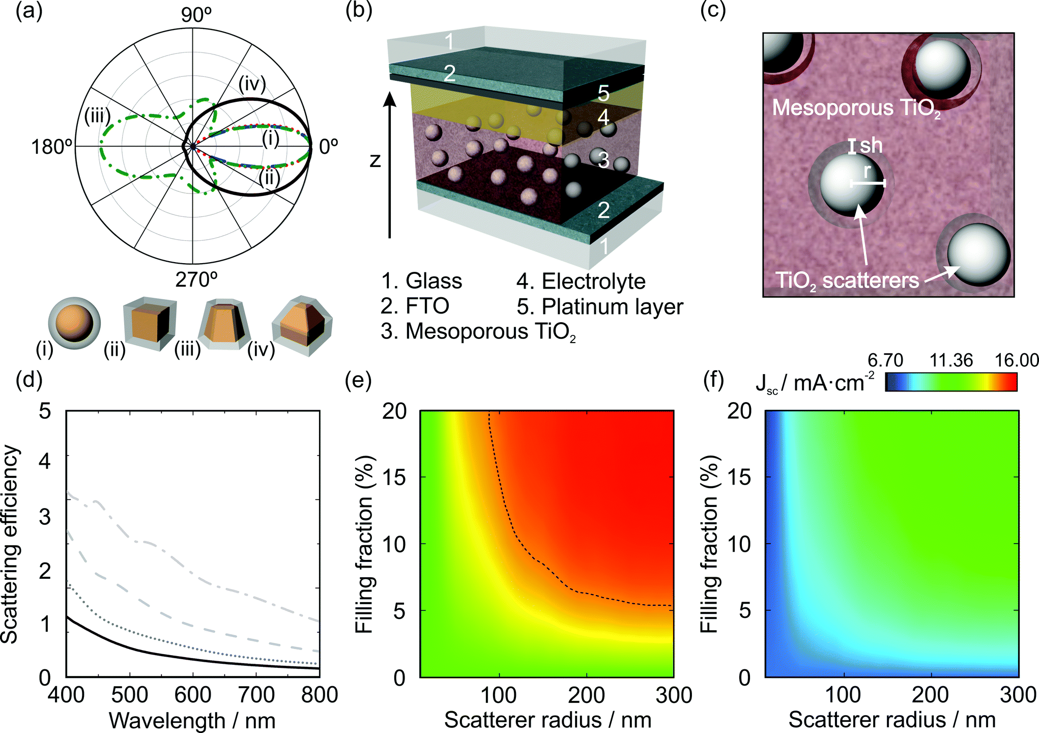 | ||
| Fig. 1 (a) FDTD calculated angular distribution of light scattered by TiO2 nanoparticles of the same volume embedded in a porous TiO2 matrix at wavelength λ = 650 nm and averaged for different orientations of the scatterers with respect to the incident light. The red dotted line corresponds to a sphere of radius r = 150 nm (i), the blue dashed line refers to a cube of side L = 242 nm (ii), the green dash-dotted line refers to a truncated pyramid of hexagonal base (iii) and the black solid line corresponds to a modified cube (iv). A shell with the same geometry as the nanoparticle filled with electrolyte is considered in all cases, with the same volume as that of a spherical shell of thickness sh = 0.5r correspondingly. (b) Schematic of the solar cell architecture including scattering centres in the mesoporous TiO2 matrix employed in the work. (c) Zoom-in of a cross-section of the active layer of the device, showing the submicron TiO2 particle system, comprised of a scattering sphere of radius r and a shell of thickness sh, embedded in the mesoporous titania matrix. (d) Mie scattering efficiency spectra of spherical TiO2 scattering centres with different sizes: r = 80 nm (solid black line), 100 nm (dotted grey line), 135 nm (dashed grey line), and 200 nm (dot-dashed grey line) and sh = 0.5r filled with the electrolyte, all embedded in a porous TiO2 matrix. (e) and (f) Upper limits for the short-circuit current density of a simulated device under front and rear illumination, respectively, in relation to the filling fraction percentage and the radius value of the scattering centres. The black dashed line in panel (e) indicates the points of Jsc = 14.20 mA cm−2 corresponding to a device including a back-scattering layer. This same line is not included in panel (f) due to its low value, 3.87 mA cm−2, which is evidently below that for the reference cell. | ||
As displayed in Fig. 1(b), the system herein investigated consists of a mesoporous TiO2 matrix incorporating spherical scattering centres and immersed in an electrolyte, sandwiched between front and rear glass/FTO contacts, the latter being coated with a thin catalytic platinum layer. A zoom-in schematic of a cross-section of the electrode is visible in Fig. 1(c), in which individual core–shell spheres are surrounded by the mesoporous TiO2 matrix. We presume that this shell originates as a consequence of the shrinking of the nanocrystalline TiO2 spheres during the sintering process of the film, as it can be seen in the Scanning Electron Microscopy (SEM) images displayed in Fig. 2. The optical effect of this shell is discussed in Fig. S4 of the ESI.†
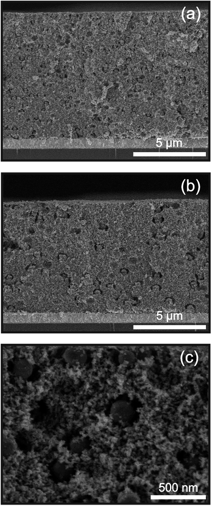 | ||
| Fig. 2 Scanning electron microscopy images of 8 μm porous TiO2 electrodes embedded with TiO2 nanospheres of (a) 10% filling fraction and 100 ± 15 nm scatterer radius, and (b) 10% filling fraction and 200 ± 25 nm scatterer radius. (c) Zoom-in of an electrode including TiO2 scatterers of radius 100 ± 15 nm. | ||
A plot of the scattering efficiencies of TiO2 spheres with four different radii: 80 nm, 100 nm, 135 nm and 200 nm is presented in Fig. 1(d). In this range, the bigger the spheres are, the more efficient they become at scattering light. We have calculated (see Methods) the expected Jsc values for a system comprising an 8 μm thick electrode containing spherical nanocrystalline TiO2 inclusions of different sizes and in different concentrations under front, Fig. 1(e), and rear, Fig. 1(f), illumination. Data for scatterer sizes up to r = 300 nm and with filling fractions up to 20% are shown. The optimum configuration can be already met between these two upper limits for r = 180 nm and ffv = 19%, with Jsc = 15.62 mA cm−2 and Jsc = 10.90 mA cm−2 being the maximum values attainable for front and rear illumination, respectively. So, according to these calculations, an enhancement around 35% in the upper limit value of Jsc can be expected under operation by front illumination, and around 40% for rear, when compared to a bare cell with no scattering centres (ffv = 0%). Note that the addition of the Jsc values yielded by a device integrating a back scattering layer, Jsc = 14.20 mA cm−2 for front illumination, included as a dashed line in Fig. 1(e), and Jsc = 3.87 mA cm−2 for the rear, is close to that for a reference cell, which yields 11.69 mA cm−2 (front) and 7.83 mA cm−2 (rear). The comparison with a hypothetical system in which the angular distribution of the scattered light is assumed to be isotropic, while the scattering and absorption efficiencies are taken according to scattering Mie theory (Fig. S5 in the ESI†), demonstrates the importance of attaining a narrow forward-oriented scattering angular distribution to maximize the performance of the device, since just a maximum of 13% and 14% enhancement for front and rear operation, respectively, in comparison to a reference cell, are expected.
Implementation of light scattering elements according to our proposed approach is possible by solution processing in a fast and inexpensive way. Moreover, the TiO2 nanospheres can be easily synthesized by sol–gel procedures that offer a precise control of their size. The random nature of this approximation makes the light scattering effect to be highly independent of the incident light angle and illumination side.27–30 On top of this, the lack of order in the integration of the inclusions reduces the complexity of the fabrication process.
Electrodes containing different filling fractions of spherical scatterers of different sizes were prepared. In Fig. 2, three SEM images show the cross section of two 8 μm thick electrodes containing TiO2 nanospheres with two different radii, namely, 100 nm and 200 nm and ffv = 10% for both. We noticed the presence of a shell around the scatterers in all cases. Fig. 2(c) provides a closer look at the film structure. SEM images of electrodes with varying filling fractions and sphere sizes are included in the ESI (see Fig. S6†). In order to check the influence of both parameters, two sets of samples were prepared: one set with the value of the scatterer radius fixed at 100 ± 15 nm and variable filling fractions ranging from 5% to 15%, and another set with 10% filling fraction and the scatterer radius ranging from 100 to 200 nm. Fig. 3(a) and (c) present the absorptance curves obtained for this system when illuminated from the rear side, that is, light impinging directly on the electrode. The films were screen printed on FTO/glass substrates. In all cases, we observe a broadband enhancement of the absorptance in the wavelength range comprised between ca. 600 nm and ca. 750 nm. Such an increase results to be larger as the value of the given parameter, either the filling fraction or scattering centre radius, becomes higher. The absorptance spectrum of a system with an electrode devoid of scattering centres has been included as a reference. Absorptance curves under front and rear illumination for a similar sample including a back scattering layer are shown as well for the sake of comparison. The corresponding theoretical curves are presented in panels 3(b) and (d), in which the sphere radius is taken to be r = 80 nm. The spherical nature of our dielectric scatterers, along with the fact that the nanoparticles are randomly distributed within the active layer, leads to an absorption enhancement that is independent of the illumination side (see Fig. S7 of the ESI†).
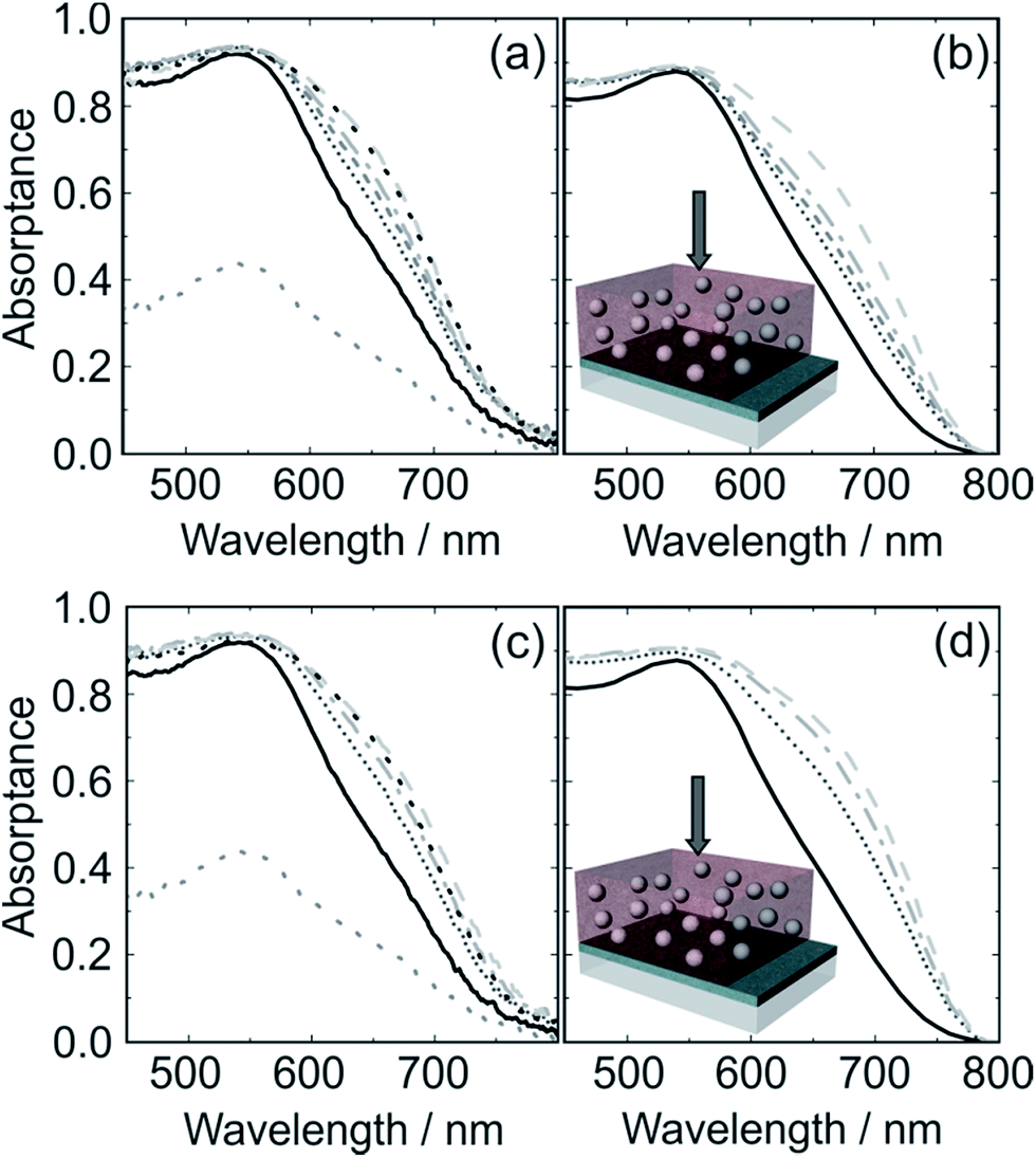 | ||
| Fig. 3 Absorptance curves of the system glass/FTO/8 μm electrode under rear illumination. (a) Experimental curves for different filling fraction values and 100 ± 15 nm scatterer radius. (b) Theoretical curves for different filling fraction values and 100 nm scatterer radius. Solid black line: reference, short-dotted grey line: ffv = 5%, short-dashed grey line: ffv = 7.5%, dash-dotted grey line: ffv = 10%, and dashed grey line: ffv = 20%. (c) Experimental curves for different sphere radii and 10% filling fraction. (d) Theoretical curves for different sphere radii and 10% filling fraction. Solid black line: reference, short-dotted grey line: 100 ± 15 nm radius, dash-dotted grey line: 135 ± 15 nm radius, and dashed grey line: 200 ± 25 nm radius. Data regarding the absorptance in a system with no inclusions and a back scattering layer are included in (a) and (c), the black dotted line being the absorptance of the system under front illumination and the grey dotted line the absorptance under rear illumination. | ||
We built solar cells for which the maximum Jsc is forecast following the predictions in panels 1(e) and (f) in Fig. 1. Measurements of the ηIPCE as a function of ffv were performed for both front and rear illumination, and are displayed in Fig. 4(a) and (b), respectively. A broadband enhancement when compared to the reference cells is observed. This improvement in the ηIPCE is visible mainly in the spectral range comprised between ca. 600 nm and 750 nm, as expected from the absorptance measurements presented in Fig. 3. It is important to notice how the trends observed under either front or rear illumination are qualitatively identical. The J–V characteristics of the devices obtained for front and rear illumination when varying ffv are also shown in Fig. 4(c) and (d), respectively. The curve corresponding to a cell including a back scattering layer is also presented for the sake of comparison. The inclusion of scattering centres leads to a significant enhancement in the value of Jsc, thus improving the performance of the device. Although these results exemplify well the effect of the approach herein proposed on the performance under both front and rear illumination, more details on the relationship between the film structure, optical properties and photovoltaic parameters can be found in the ESI (see Fig. S8 and S9†).
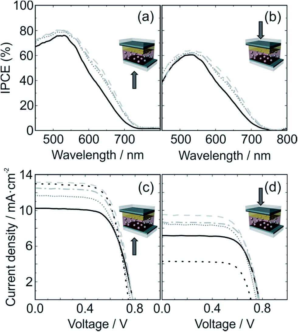 | ||
| Fig. 4 Experimental incident photon to current efficiency (ηIPCE) and current density–voltage (J–V) curves for complete cells with different filling fraction values and 160 ± 50 nm scatterer radius. (a) ηIPCE curves for front illumination. (b) ηIPCE curves for rear illumination. (c) J–V characteristics for front illumination. (d) J–V characteristics for rear illumination. Solid black line: reference, short-dotted grey line: ffv = 5%, dash-dotted grey line: ffv = 10%, dashed grey line: ffv = 15%, and dotted black line: cell with a back scattering layer. Electrode thickness: 8 μm. | ||
The results obtained for several sets of cells by varying the two given parameters, shown in Table 1, were averaged and only a representative curve of each type is shown for clarity. The observed trend is in accordance with that expected from the absorptance and ηIPCE curves. PCEs are always above the ca. 5.4% attained for the bare reference cells under front illumination. Such enhancement is, in turn, larger as the filling fraction or the sphere radius increases. A maximum efficiency of 6.7% associated with an averaged Jsc = 13.54 mA cm−2 is measured for the device including 200 nm radius nanocrystalline TiO2 spheres with ffv = 10% for front illumination, which corresponds to a theoretically estimated scattering mean free path lsc = 1.2 μm at λ = 650 nm. Such a short value, in comparison to the electrode thickness (8 μm), is consistent with the experimental observation of an enhancement of the absorptance. This means that several scattering events will occur before the light reaches the opposite side of the sensitized film. As a consequence, the path length of the light is increased and thus the probability for the incident radiation to be absorbed. The aforementioned efficiency improvement corresponds to a 25% enhancement with respect to the reference cell. Furthermore, this performance is above that observed from the measurements performed on cells including a back scattering layer under front illumination, with an averaged Jsc = 12.70 mA cm−2 and an efficiency of 6.3%, showing the potential for competitiveness of the approach herein proposed when compared to other standard methods for light harvesting enhancement that are valid only for one-side illumination. Lower Jsc values are measured under rear-side operation, as expected, due to the smaller fraction of the incident light reaching the active layer owing to the additional layers absorbing and reflecting light, e.g., the thin catalytic platinum layer and the electrolyte layer, the latter presenting a significant absorptance peak near λ = 400 nm. Specifically, under rear illumination, a maximum Jsc = 10.40 mA cm−2 is measured for the device including 200 nm radius spherical scatterers with ffv = 10%, corresponding to a 5.4% PCE, which represents a 33% enhancement with respect to a bare cell. The measured Jsc values increase with both the filling fraction and the scatterer size, displaying the same trend observed under front illumination. In contrast, the performance of devices including a back scattering layer strongly decreases for rear illumination, showing a limited 2.1% efficiency. Interestingly, if the use of thicker (≈15 μm) sensitized films as those typically employed to achieve high efficiency bifacial cells is regarded as an option, our model predicts a rear and front side enhancement above 20%.
| Sample | Illumination | J sc exp. mA cm−2 | V oc mV | FF (%) | PCE (%) | η rear/ηfront | |
|---|---|---|---|---|---|---|---|
| ffv (r = 160 ± 50 nm) | Reference | Front | 10.30 ± 0.06 | 780 ± 2 | 65.6 ± 0.8 | 5.3 ± 0.0 | 0.72 ± 0.00 |
| Rear | 7.19 ± 0.02 | 773 ± 4 | 69.3 ± 0.2 | 3.8 ± 0.0 | |||
| ffv = 5% | Front | 11.50 ± 0.30 | 764 ± 4 | 63.8 ± 0.8 | 5.6 ± 0.1 | 0.74 ± 0.11 | |
| Rear | 8.20 ± 0.30 | 752 ± 1 | 67.1 ± 0.3 | 4.2 ± 0.2 | |||
| ffv = 10% | Front | 12.40 ± 0.30 | 784 ± 6 | 64.4 ± 0.4 | 6.2 ± 0.1 | 0.74 ± 0.09 | |
| Rear | 8.68 ± 0.16 | 779 ± 5 | 68.1 ± 0.6 | 4.6 ± 0.1 | |||
| ffv = 15% | Front | 12.90 ± 0.30 | 782 ± 5 | 65.3 ± 1.1 | 6.6 ± 0.1 | 0.74 ± 0.08 | |
| Rear | 9.30 ± 0.40 | 768 ± 4 | 68.1 ± 0.8 | 4.9 ± 0.2 | |||
| Back scattering layer | Front | 12.70 ± 0.40 | 762 ± 8 | 64.6 ± 0.4 | 6.3 ± 0.1 | 0.34 ± 0.03 | |
| Rear | 4.02 ± 0.06 | 737 ± 8 | 71.8 ± 0.4 | 2.1 ± 0.0 | |||
| Size (ffv = 10%) | Reference | Front | 11.02 ± 0.21 | 750 ± 5 | 65.1 ± 1.0 | 5.4 ± 0.4 | 0.75 ± 0.07 |
| Rear | 8.00 ± 0.40 | 744 ± 6 | 68.4 ± 0.9 | 4.1 ± 0.2 | |||
| r = 100 ± 15 nm | Front | 12.70 ± 0.60 | 761 ± 1 | 63.2 ± 1.1 | 6.1 ± 0.1 | 0.77 ± 0.06 | |
| Rear | 9.20 ± 0.05 | 750 ± 2 | 67.0 ± 0.6 | 4.7 ± 0.1 | |||
| r = 135 ± 15 nm | Front | 12.96 ± 0.14 | 762 ± 4 | 64.4 ± 1.4 | 6.4 ± 0.1 | 0.78 ± 0.09 | |
| Rear | 9.80 ± 0.30 | 753 ± 2 | 67.7 ± 1.1 | 5.0 ± 0.1 | |||
| r = 200 ± 25 nm | Front | 13.54 ± 0.12 | 769 ± 7 | 64.3 ± 0.5 | 6.7 ± 0.1 | 0.80 ± 0.11 | |
| Rear | 10.40 ± 0.30 | 766 ± 6 | 67.5 ± 0.5 | 5.4 ± 0.1 |
Experimental observations indicate that there exists a maximum value of the volume occupied by the inclusions before the film suffers from mechanical instability or delamination. Consequently, it was not possible to fabricate electrodes containing big particles in a large loading fraction. However, the values attained within the limits imposed by fabrication are close to those found as optimal.
The values of the open circuit voltage (Voc) and fill factor (FF) of the cells scarcely fluctuate, around Voc = 760 mV and FF = 65% under front illumination, and Voc = 750 mV and FF = 68% under rear illumination. Notice that such electrical parameters are in line with those for the state-of-the-art cells employing platinum as the catalytic material.10,13–17,19 In particular, the Jsc and PCE values attained for rear illumination are above most of those reported for this standard configuration of the cell, in spite of the fact that the active layers herein employed are approximately 50% thinner than the ones for which the largest efficiencies attained are reported.10,12,13,15–17,19,21 Hence, a direct consequence of optimising the optical design of the bifacial cell is that we can reduce significantly the electrode thickness.
The independence of the enhancement achieved on the illumination side becomes even more visible when peering at the rear/front efficiency ratios in the last column of Table 1, which barely vary. This points out that the front and rear efficiencies increase with the particle size and loading in a similar way regardless of the illumination conditions, indicating that the fabricated devices operate as improved bifacial cells. Such values prove that our design is an effective route toward efficient bifacial performance, being amongst the largest values reported in the literature to date for cells employing Pt as the material for the coating of the counter-electrode, and standard (<10 μm) film thickness.11–20 Moreover, most of the approaches reported in the literature to improve the efficiency of bifacial cells are compatible with the electrode modification we proposed herein.
The experimental values attained for the Jsc were contrasted with the upper limit predicted by the model, from which a collection efficiency value near 90% could be estimated, consistent with the 18 μm electron diffusion length theoretically assessed from the fitting of the experimental ηIPCE curves (please see Fig. S10 and S11 in the ESI†). Most importantly, the inclusion of the nanocrystalline scatterers does not entail a significant decrease of the collection efficiency, which means that they do not affect charge transport as it has been demonstrated in other systems including elements causing light scattering by means of Electrical Impedance Spectroscopy.51,52 Implementation of our approach has therefore no detrimental influence in the electrical properties of the devices.
A modification of the optical design implies a change in the spatial distribution of absorbed light within the electrode. We have calculated the light absorption profile, also known as the electron generation function, in the active layer of a reference cell and of a cell including scatterers. Fig. 5 shows the absorption per unit length along the z direction, defined in Fig. 1(b), in an 8 μm thick electrode of a reference cell under front, Fig. 5(a), and rear, Fig. 5(b), illumination, and that for a cell containing 160 nm radius spheres and ffv = 15% under front, Fig. 5(c), and rear, Fig. 5(d), illumination. When comparing Fig. 5(c) with 5(a) and Fig. 5(d) with 5(b), we observe that light absorption is boosted in both cases, especially in the ca. 600 nm to ca. 750 nm range. Light harvesting is increased in regions close to the photoanode under front illumination, which might be a potential profit for devices in which the electron collection efficiency is low, as generation at distances closer to the contacts involves lower recombination probability.
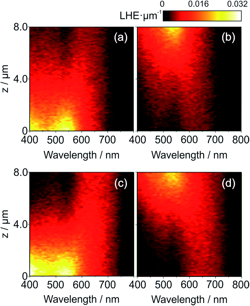 | ||
| Fig. 5 Absorption profiles as a function of the wavelength of the dye along the sensitized film for a 8 μm thick reference electrode under (a) front, and (b) rear illumination, and a cell with TiO2 spherical inclusions of 160 nm radius and 15% filling fraction under (c) front and (d) rear illumination. | ||
Conclusions
We have developed a combined theoretical and experimental approach for the fabrication of efficient bifacial DSSCs through the random dispersion of spherical TiO2 scattering centres in their photoanodes. As a consequence, absorption was boosted regardless of the illumination direction in the red part of the visible spectrum, where the absorption cross-section of the commonly used N719 dye is low. Electrical characterization of the devices revealed a significant enhancement of the Jsc value, and thus, efficiency both under front and rear illumination. The random nature of the approach makes the enhancement independent of the direction of the illumination of incoming light, which is evidenced by the high rear to front efficiency ratio values. Using only standard cell components, and playing only with the optical design, we were able to obtain values of the relevant photovoltaic parameters in line with those reported for state-of-the-art bifacial cells, which make use of at least 50% thicker electrodes than the ones herein considered and of modified counter-electrodes. In this regard, the optically optimized working electrode herein proposed is compatible with any complementary method for performance improvement under rear illumination. Our approach may be applied to the fabrication of other systems in which finely tuned disorder may prove advantageous, thus offering potential benefits for the development of optoelectronic devices for which an accurate control of light absorption and emission is desired.Acknowledgements
Funding for the development of the research leading to these results was received from the European Research Council under the European Union's Seventh Framework Programme (FP7/2007-2013)/ERC grant agreement no. 307081 (POLIGHT) and the Spanish Ministry of Economy and Competitiveness under grant MAT2014-54852-R. JMMM acknowledges the Spanish Ministry of Education, Culture and Sport for the funding through an FPU program. AJS acknowledges the Spanish Ministry of Economy and Competitiveness for funding through an FPI program under the project MAT2011–23593. YL acknowledges the funding from the People Programme (Marie Curie Actions) of the European Union's Seventh Framework Programme FP7/2007-2013/under REA grant agreement no. 622533.Notes and references
- B. O'Regan and M. Grätzel, Nature, 1991, 353, 737 CrossRef.
- G. Niu, W. Li, F. Meng, L. Wang, H. Dong and Y. Qiu, J. Mater. Chem. A, 2014, 2, 705 CAS.
- K. Wang, W. He, L. Wu, G. Xu, S. Ji and C. Ye, RSC Adv., 2014, 4, 15702 RSC.
- G. Xue, Y. Guo, T. Yu, J. Guan, X. Yu, J. Zhang, J. Lin and Z. Zou, Int. J. Electrochem. Sci., 2012, 7, 1496 CAS.
- R. Kern, N. van der Burg, G. Chmiel, J. Ferber, G. Hasenhindl, A. Hinsch, R. Kinderman, J. Kroon, A. Meyer, T. Meyer, R. Niepmann, J. van Roosmalen, C. Schill, P. Sommeling, M. Späth and I. Uhlendorf, Opto-Electron. Rev., 2000, 8, 284 CAS.
- A. Hinsch, J. M. Kroon, R. Kern, I. Uhlendorf, J. Holzbock, A. Meyer and J. Ferber, Prog. Photovoltaics, 2001, 9, 425 CAS.
- A. Kay and M. Grätzel, Sol. Energy Mater. Sol. Cells, 1996, 44, 99 CrossRef CAS.
- A. Fakharuddin, R. Jose, T. M. Brown, F. Fabregat-Santiago and J. Bisquert, Energy Environ. Sci., 2014, 7, 3952 CAS.
- A. Hübner, A. G. Aberle and R. Hezel, Appl. Phys. Lett., 1997, 70, 1008 CrossRef.
- S. Ito, S. M. Zakeeruddin, P. Comte, P. Liska, D. Kuang and M. Grätzel, Nat. Photonics, 2008, 2, 693 CrossRef CAS.
- X. Li, Z. Ku, Y. Rong, G. Liu, L. Liu, T. Liu, M. Hu, Y. Yang, H. Wang, M. Xu, P. Xiang and H. Han, Phys. Chem. Chem. Phys., 2012, 14, 14383 RSC.
- Y. Rong, Z. Ku, X. Li and H. Han, J. Mater. Sci., 2015, 50, 3803 CAS.
- H. Cai, Q. Tang, B. He, R. Li and L. Yu, Nanoscale, 2014, 6, 15127 RSC.
- Y. Duan, Q. Tang, J. Liu, B. He and L. Yu, Angew. Chem., Int. Ed., 2014, 53, 14569 CrossRef CAS PubMed.
- Y. Duan, Q. Tang, B. He, R. Li and L. Yu, Nanoscale, 2014, 6, 12601 RSC.
- J. Liu, Q. Tang, B. He and L. Yu, J. Power Sources, 2015, 275, 288 CrossRef CAS.
- D. Song, M. Li, Y. Li, X. Zhao, B. Jiang and Y. Jiang, ACS Appl. Mater. Interfaces, 2014, 6, 7126 CAS.
- Q. Tai, B. Chen, F. Guo, S. Xu, H. Hu, B. Sebo and X. Zhao, ACS Nano, 2011, 5, 3795 CrossRef CAS PubMed.
- J. Wu, Y. Li, Q. Tang, G. Yue, J. Lin, M. Huang and L. Meng, Sci. Rep., 2014, 4, 4028 Search PubMed.
- S. Xu, Y. Luo, G. Liu, G. Qiao, W. Zhong, Z. Xiao, Y. Luo and H. Ou, Electrochim. Acta, 2015, 156, 20 CrossRef CAS.
- H. Zhang, B. He, Q. Tang and L. Yu, J. Power Sources, 2015, 275, 489 CrossRef CAS.
- N. Fu, Y. Fang, Y. Duan, X. Zhou, X. Xiao and Y. Lin, ACS Nano, 2012, 6, 9596 CrossRef CAS PubMed.
- N. C. Jeong, C. Prasittichai and J. T. Hupp, Langmuir, 2011, 27, 14609 CrossRef CAS PubMed.
- X. Dang, J. Qi, M. T. Klug, P. Chen, D. S. Yun, N. X. Fang, P. T. Hammond and A. M. Belcher, Nano Lett., 2013, 13, 637 CrossRef CAS PubMed.
- K. Guo, M. Li, X. Fang, X. Liu, B. Sebo, Y. Zhu, Z. Hu and X. Zhao, J. Power Sources, 2013, 230, 155 CrossRef CAS.
- S. Colodrero, A. Mihi, L. Häggman, M. Ocaña, G. Boschloo, A. Hagfeldt and H. Míguez, Adv. Mater., 2009, 21, 764 CrossRef CAS.
- J. Kim, J. K. Koh, B. Kim, J. H. Kim and E. Kim, Angew. Chem., Int. Ed., 2012, 51, 6864 CrossRef CAS PubMed.
- S. Wooh, H. Yoon, J. Jung, Y. Lee, J. H. Koh, B. Lee, Y. S. Kang and K. Char, Adv. Mater., 2013, 25, 3111 CrossRef CAS PubMed.
- D. Barettin, A. Di Carlo, R. de Angelis, M. Casalboni and P. Prosposito, Opt. Express, 2012, 20, A888 CrossRef PubMed.
- C. López-López, S. Colodrero, A. Jiménez-Solano, G. Lozano, R. Ortiz, M. E. Calvo and H. Míguez, Adv. Opt. Mater., 2014, 2, 879 CrossRef.
- C. López-López, S. Colodrero and H. Míguez, Phys. Chem. Chem. Phys., 2013, 16, 663 RSC.
- A. Usami, Chem. Phys. Lett., 1997, 277, 105 CrossRef CAS.
- M. Son, H. Seo, S. Kim, N. Hong, B. Kim, S. Park, K. Prabakar and H. Kim, Int. J. Photoenergy, 2012, 480929 Search PubMed.
- S. Hore, C. Vetter, R. Kern, H. Smit and A. Hinsch, Sol. Energy Mater. Sol. Cells, 2005, 90, 1176 CrossRef.
- H. Koo, J. Park, B. Yoo, K. Yoo, K. Kim and N. Park, Inorg. Chim. Acta, 2007, 361, 677 CrossRef.
- Z. Wang, H. Kawauchi, T. Kashima and H. Arakawa, Coord. Chem. Rev., 2004, 248, 1381 CrossRef CAS.
- A. Usami, Sol. Energy Mater. Sol. Cells, 2000, 64, 73 CrossRef CAS.
- J. Ferber and J. Luther, Sol. Energy Mater. Sol. Cells, 1998, 54, 265 CrossRef CAS.
- F. E. Gálvez, E. Kemppainen, H. Míguez and J. Halme, J. Phys. Chem. C, 2012, 116, 11426 Search PubMed.
- Y. Chiba, A. Islam, Y. Watanabe, R. Komiya, N. Koide and L. Han, Jpn. J. Appl. Phys., 2006, 45, L638 CrossRef CAS.
- Y. Tachibana, K. Hara, K. Sayama and H. Arakawa, Chem. Mater., 2002, 14, 2527 CrossRef CAS.
- C. J. Barbé, F. Arendse, P. Comte, M. Jirousek, F. Lenzmann, V. Shklover and M. Grätzel, J. Am. Ceram. Soc., 1997, 80, 3157 CrossRef.
- S. H. Kang, J. Kim, H. S. Kim, H. Koh, J. Lee and Y. Sung, J. Photochem. Photobiol., A, 2008, 200, 294 CrossRef CAS.
- H. Arakawa, T. Yamaguchi, T. Sutou, Y. Koishi, N. Tobe, D. Matsumoto and T. Nagai, Curr. Appl. Phys., 2009, 10, S157 CrossRef.
- Y. Li, K. Yoo, D. Lee, J. Y. Kim, H. J. Son, J. H. Kim, C. Lee, H. Míguez and M. J. Ko, RSC Adv., 2015, 5, 76795 RSC.
- G. Mie, Ann. Phys., 1908, 330, 377 CrossRef.
- I. W. Suidarta and P. Chylek, J. Opt. Soc. Am. A, 2001, 18, 1275 CrossRef.
- G. Rothenberger, P. Comte and M. Grätzel, Sol. Energy Mater. Sol. Cells, 1999, 58, 321 CrossRef CAS.
- F. E. Gálvez, P. R. F. Barnes, J. Halme and H. Míguez, Energy Environ. Sci., 2014, 7, 689 Search PubMed.
- Y. J. Kim, M. H. Lee, H. J. Kim, G. Lim, Y. S. Choi, N. Park, K. Kim and W. I. Lee, Adv. Mater., 2009, 21, 1 Search PubMed.
- G. Lee, H. Lee, M. Um and M. Kang, Bull. Korean Chem. Soc., 2012, 33, 3043 CrossRef CAS.
- J. Durantini, P. P. Boix, M. Gervaldo, G. M. Morales, L. Otero, J. Bisquert and E. M. Barea, J. Electroanal. Chem., 2012, 683, 43 CrossRef CAS.
Footnote |
| † Electronic supplementary information (ESI) available. See DOI: 10.1039/c5ta10091g |
| This journal is © The Royal Society of Chemistry 2016 |