
 Open Access Article
 This Open Access Article is licensed under a
 Creative Commons Attribution 3.0 Unported Licence
Relativistic electronic structure and band alignment of BiSI and BiSeI: candidate photovoltaic materials†
Alex M.
Ganose
ab,
Keith T.
Butler
c,
Aron
Walsh
cd and
David O.
Scanlon
*ab
aUniversity College London, Kathleen Lonsdale Materials Chemistry, Department of Chemistry, 20 Gordon Street, London, WC1H 0AJ, UK. E-mail: d.scanlon@ucl.ac.uk
bDiamond Light Source Ltd., Diamond House, Harwell Science and Innovation Campus, Didcot, Oxfordshire OX11 0DE, UK
cCentre of Sustainable Chemical Technology and Department of Chemistry, University of Bath, Claverton Down, Bath BA2 7AY, UK
dGlobal E3 Institute and Department of Materials Science and Engineering, Yonsei University, Seoul 120-749, Korea
First published on 14th January 2016
Abstract
Bismuth-based solar absorbers are of interest due to similarities in the chemical properties of bismuth halides and the exceptionally efficient lead halide hybrid perovskites. Whilst they both experience the same beneficial relativistic effects acting to increase the width of the conduction band, bismuth is non-toxic and non-bioaccumulating, meaning the impact of environmental contamination is greatly reduced. Here, we use hybrid density functional theory, with the addition of spin orbit coupling, to examine two candidate bismuth containing photovoltaic absorbers, BiSI and BiSeI, and show that they possess electronic structures suitable for photovoltaic applications. Furthermore, we calculate band alignments against commonly used hole transporting and buffer layers, which indicate band misalignments are likely to be the source of the poor efficiencies reported for devices containing these materials. Based on this we have suggested alternative device architectures expected to result in improved power conversion efficiencies.
As the global demand for energy continues to grow inexorably, there is an increasing need for a clean energy source capable of providing indefinite and sustainable economic growth. With a year’s worth of sunlight providing almost two hundred times the energy of the world's entire known supply of fossil fuels, solar power is suitably positioned as a strong contender for utility-scale power generation.1,2 Currently, the photovoltaic (PV) market is dominated by crystalline silicon panels, which, whilst relatively efficient, are subject to high synthesis and processing costs, limiting their potential for widespread application.3,4 Other technologies, such as those containing Cu(In/Ga)Se2 (CIGS) and CdTe absorbers, show efficiencies approaching 22% (ref. 5 and 6) but contain cadmium, which is toxic and indium, the price of which is highly volatile due to the limited number of suppliers.7
The last 10 years have therefore seen a significant research drive into low-cost materials containing only earth-abundant elements,8–11 termed third-generation devices, from which hybrid halide perovskites emerged as a promising class of solar absorbers in 2009.12,13 Currently, the highest performing hybrid perovskite is CH3NH3PbI3 (MAPI), which can be easily solution processed allowing for dramatically reduced manufacturing costs.14–16 Impressively, the power conversion efficiencies (PCEs) of MAPI-based devices have quickly overtaken all other third-generation absorbers such as Cu2ZnSn(S,Se)4 (ref. 17) and dye-sensitised solar cells,18 reaching 20.1% in only 6 years.19,20 Unfortunately, the intrinsic stability of MAPI is still unresolved, and observations of facile decomposition upon contact with moisture have lead to concerns over long-term performance and the potential environmental risks due to leaching of toxic Pb.21–23 There is therefore an urgent need to explore novel materials capable of replicating the significant successes of hybrid perovskites, whilst employing rational design in order to prevent similar shortcomings.
Recently, bismuth-based PV materials have become of interest, in part due to similarities in the chemical properties of bismuth halides and lead hybrid perovskites.24–26 Both Pb2+ and Bi3+ adopt a stable d10s2p0 electronic configuration,27 possess a similar soft polarisability and form a wide range of compounds with rich structural diversity,28,29 such as BiX6 clusters,25 1D ribbons,30 and layered perovskite type structures.26,31 Bismuth containing compounds also experience the same beneficial large relativistic effects seen in MAPI, which act to stabilise the material against oxidation and increase the conduction band width through a significant lowering of the conduction band minimum (CBM).32–34 Importantly, bismuth is non-toxic and non-bioaccumulating, meaning the impact of environmental contamination is greatly reduced.35,36 Whilst an increasing number of bismuth halides have been screened for solar absorber properties in recently months, such as BiI3 (ref. 26 and 37) and A3Bi2I9 (where A = K or Rb,25 Cs or CH3NH3,38 and NH4 (ref. 39)), research into the electronic properties of complex bismuth halides remains limited. As such, these compounds present an understudied class of earth-abundant and non-toxic materials, with significant potential in PV applications.
Two such materials displaying promise as solar absorbers are BiSI and BiSeI.24 Both crystallise in the ribbon structure shown in Fig. 1, in which [(BiChI)∞]2 ribbons are held together by weak ionic or van der Waals-type forces (Fig. 1).30,40 Recently, Zhou et al. have proposed that this type of geometry can provide several advantages: (i) by orientating the crystal such that the ribbons are vertically aligned on the substrate, a clear pathway is formed between the device contacts allowing for efficient carrier transport along the covalently bonded 1D axis, and (ii) by enforcing vertically aligned growth, any grain boundaries should occur parallel to the ribbons and therefore will not result in dangling bonds, substantially minimising recombination losses.41 Furthermore, alloying of BiSI with BiSeI should not disrupt the connectivity of the conduction pathways and will simultaneously allow for precise tuning of the band gap.42 These advantages have recently been demonstrated in another 1D solar absorber, Sb2Se3, in which controlled growth of a vertically aligned film resulted in an increase in efficiency of over 2%, when compared to orientations that produced dangling bonds at grain boundaries.41
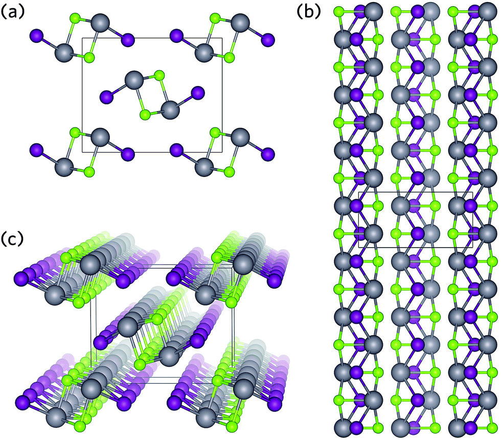 | ||
| Fig. 1 Crystal structure of BiSeI as viewed along (a) the [100] direction, (b) the [001] direction, and (c) a three-dimensional view, highlighting the 1D chains. Bi, Se, and I atoms are denoted by grey, green, and purple spheres, respectively. | ||
In 2012, Hahn et al. screened BiSI and BiSeI for PV applications, finding them to be n-type materials, with high absorption coefficients and indirect band gaps of 1.57 eV and 1.29 eV, respectively.42,43 However, an extremely low PCE (0.012%) was observed when BiSI was incorporated into a device containing CuSCN as a p-type hole transporting material and fluorine-doped tin oxide (FTO) as the front contact. The authors note that hole diffusion lengths in BiSI samples were only 50 nm43 and propose that effective screening of the electric field at the heterojunction prevents efficient electron–hole separation, resulting in high levels of charge-carrier recombination in the neutral bulk. This is, however, in contrast to other materials with large dielectric constants, such as MAPI, where this screening does not appear to negatively affect charge separation and has instead been lauded as providing enhanced defect tolerance.24,44,45 Instead, it is likely that the polycrystalline nature of the films used in these devices precludes the formation of clear pathways for charge-carrier extraction and undermines the proposed benefits of the ribbon structure. Regardless, these materials appear to possess many of the desired properties of efficient solar absorbers and, as such, warrant further analysis.
In this letter we study the fundamental electronic structure of BiSI and BiSeI, using hybrid density functional theory (DFT). We demonstrate: (i) that despite possessing indirect band gaps, in both cases the difference between the direct and indirect band gaps is small and should result in only marginal effects on performance, (ii) the valence band maximum shows largely anti-bonding character, which enhances band dispersion and may be of benefit for the defect chemistry, and (iii) the mixing of the S/Se and I p states produces a diffuse conduction band in the directions along the ribbon structure, indicating that the material should show good conductivity in these directions. Lastly, we calculate the fundamental band alignments and accordingly suggest transparent conducting oxide and hole transporting materials likely to minimise interfaces losses in order to improve device efficiencies.
Computational methods
All calculations were performed using the Vienna Ab initio Simulation Package (VASP),46–49 a periodic plane wave DFT code which includes the interactions between the core and valence elections using the Project Augmented Wave (PAW) method.50 Both the plane wave basis set and k-point sampling were checked for convergence, with a cutoff of 520 eV and k-point grid of Γ-centred 3 × 6 × 2, for the 12 atom unit cells of BiSI and BiSeI, found to be sufficient. Geometry optimisations were tested using two functionals: the Perdew, Burke and Ernzerhof (PBE) functional51 and the PBEsol functional,52 a version of PBE revised for solids. Both functionals were trialled with and without the addition of Grimme's dispersion correction (D3),53 however, we note that PBEsol often accurately predicts the lattice constants for systems containing van der Waals interactions, without the need to treat them explicitly.54 The structures were deemed to be converged when the forces on all the atoms totalled less than 10 meV Å−1. In order to accurately predict electronic properties, the Heyd–Scuseria–Ernzerhof (HSE06) hybrid DFT functional55 with the addition of spin orbit effects (SOC) was used for density of states, charge density, and band structure calculations.25,37,56,57 Crystal Orbital Hamilton Population (COHP) analysis was performed using the LOBSTER program.58,59In the plane wave formalism, due to the presence of periodic boundary conditions, the electrostatic potential of a crystal is not defined with respect to an external vacuum level and, as such, the absolute electronic eigenvalues from different calculations are not comparable. In order to align the energies to the vacuum level, a slab–gap model (20 Å slab, 20 Å vacuum) was constructed and the corresponding electrostatic potential averaged along the c-direction, using the MacroDensity package (Fig. 2).60–62 HSE06 + SOC has previously been shown to provide accurate ionisation potentials for similar systems,63 however, the large size of the surfaces precluded its use in this study. Instead the slab calculations were performed using the HSE06 functional with a correction for the valence band energy and band gap, taken from the HSE06 + SOC calculated bulk. The energy of the potential at the plateau was used as the external vacuum level when aligning the core-level eigenvalues. Based on similar work into SbSI, the (110) surface was chosen as it did not produce any dangling bonds and resulted in a low energy, non-polar termination.
 | ||
| Fig. 2 2D slab model used to align the electronic eigenvalues to the vacuum level viewed along the [010] direction. The corresponding electrostatic (Hartree) potential calculated using HSE06 is shown in blue. Bi, Se, and I atoms are denoted by grey, green, and purple spheres, respectively. | ||
Geometry
BiSI and BiSeI both crystallise in the same structure as SbSI (space group Pnma), in which BiChI ribbons resulting from distorted edge-sharing pseudo-octahedra are formed from 3 Bi–Ch and 2 Bi–I bonds, with a vacant site occupied by the Bi lone pair.30,40 Two Bi–Ch bonds lengths are observed depending on whether the bonds are parallel (Bi–Ch∥) or perpendicular (Bi–Ch⊥) to the ribbons shown in Fig. 1b. The effect of functional on geometry optimisation was tested, with the full results provided in Table S1 of the ESI.† The PBEsol functional (without the inclusion of Grimme's dispersion) best reproduced the experimental lattice parameters and bond distances (within 1%, Table 1). In both BiSI and BiSeI, the a and b parameters were underestimated suggesting thermal effects will play a role in the structure, most likely in determining the distance between ribbons.| BiSI | BiSeI | |
|---|---|---|
| a | 8.44 (−0.88%) | 8.63 (−0.83%) |
| b | 4.13 (−1.00%) | 4.19 (−0.78%) |
| c | 10.26 (+0.82%) | 10.58 (+0.06%) |
| Bi–I | 3.20 (+0.17%) | 3.23 (−0.47%) |
| Bi–Ch⊥ | 2.61 (+0.69%) | 2.74 (+0.97%) |
| Bi–Ch∥ | 2.73 (−0.36%) | 2.85 (−0.26%) |
Electronic structure
The band structures of BiSI and BiSeI are presented in Fig. 3a and c. The effect of spin orbit coupling was tested, with the results provided in Fig. S1 of the ESI.† In both cases, the relativistic renormalisation of the conduction band was found to be over 0.6 eV, highlighting the importance of including spin orbit effects in modelling these systems. The band structures show broadly the same features, with the main difference being the position of the band edges. In BiSI, the valence band maximum (VBM) and CBM occur between Y–Γ and Γ–Z, respectively, whereas in BiSeI, the VBM occurs between Γ–Z and the CBM is situated at Γ. The calculated band gaps for BiSI and BiSeI are 1.78 eV and 1.50 eV, respectively and are noticeably overestimated compared to experiment (1.57 eV and 1.29 eV for BiSI and BiSeI), which is likely due to the absence of thermal effects, including lattice expansion and electron–phonon coupling, when performing the calculations. The band gaps are both indirect (Eig), as expected of group 15 chalcohalide semiconductors,65,66 however, as the direct band gap (Edg) is more relevant for thin film solar absorbers, due to the requirement for high absorption coefficients (vertical optical transitions), it is provided in Table 2. The difference between the direct and indirect band gaps is only ∼0.1 eV, indicating that these materials are still suitable for thin film photovoltaic applications.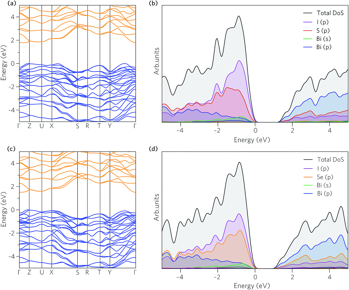 | ||
| Fig. 3 (a and c) Band structures along the high symmetry directions, and (b and d) ion decomposed partial and total density of states, for BiSI and BiSeI, respectively. In all cases the valence band maximum is set to zero eV. The valence bands and conduction bands of (a and c) are denoted by blue and orange respectively. | ||
| BiSI | BiSeI | |
|---|---|---|
| E ig (eV) | 1.78 | 1.50 |
| E dg (eV) | 1.82 | 1.60 |
| m *e (CBM → Z) | 0.69 | 4.52 |
| m *e (CBM → Γ) | 1.78 | — |
| m *e (CBM → Y) | — | 0.51 |
| m *h (VBM → Γ) | 0.51 | — |
| m *h (VBM → Y) | 0.36 | — |
| m *h (VBM → Z) | — | 0.40 |
| m *h (VBM → Γ) | — | 0.28 |
| ε r | 36.8 | 35.8 |
The partial (ion decomposed) density of states (DOS) are shown in Fig. 3b and d. The overall shape of the states is similar in both cases, with the main difference being the increase in energy of the of Se p orbital which acts to raise the VBM. The VBM is formed from mixing of I and S/Se p states with some and Bi s and p states, whilst the CBM is dominated by Bi p states with contributions from the I and S/Se p orbitals, similar to in other group 15 chalcohalide semiconductors.56
The contribution of the Bi states to the VBM can be accounted for by the Bi lone pair. Like many of the heavier metals in groups 13 to 16, the stability of the d10s2p0 electronic configuration means Bi prefers to adopt a valence state two lower than its group valence. Classical lone pair theory predicts that the formation of a stereochemically active lone pair in BiSI results from on-site hybridisation of non-bonding Bi s and Bi p states close to the Fermi level.67,68 However, similar to other metal–non-metal systems with partially oxidised cations, such as PbS69 and CuBiCh2,8 these cation s states occur too far below the VBM for hybridisation to occur (approximately −11 eV below the VBM in BiSI and BiSeI). Instead, mixing of metal s states with anion p states results in filled bonding and anti-bonding states at the bottom and top of the valence band, respectively, as indicated in the COHP analysis given in Fig. S2 of the ESI.†,27 It has recently been suggested that these anti-bonding states help to ensure that dangling bonds, formed upon vacancy formation, will appear as resonances in the valence bands, significantly improving point defect tolerance.70,71
If these anti-bonding states contain a substantial cation s contribution, they can mix with unoccupied cation p states at the top of the valence band, resulting in a significant stabilisation effect. It is this interaction which produces the asymmetric electron density responsible for the distortion of the pseudo-octahedra.72–74 This effect is primarily mediated by the relative energies of the cation s and anion p states, as states closer in energy will increase the cation s contribution at the top of the valence band and result in stronger lone pairs.27 As such, the lone pair effect is most prominent in oxides and lessens down the chalcogen group. A further reduction in lone pair strength is seen in Bi compounds due to the reduction in energy of the Bi 6 s states due to the scalar-relativistic contraction of the s-shell.27,75 Consequently, BiSI and BiSeI possess lone pairs that are relatively diffuse, as evidenced by the charge density isosurfaces presented in Fig. 4, which show low electron density around the Bi ions at the top of the valence band. The strength of the lone pair is also indicated by the degree of pseudo-octahedral distortion in the lattice and can be calculated as the average deviation in the bond angles of the BiChI pseudo-octahedra from the ideal angle of 90°, σoct. As expected, the distortion is seen to decrease when moving from BiSI to BiSeI, from 7.49° to 6.61°, respectively. We note that this distortion is significantly less than in materials with strongly stereoactive lone pairs, such as Sb2O3 (σoct = 21.82°).76
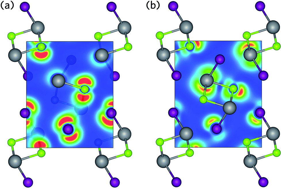 | ||
| Fig. 4 Charge density isosurfaces of (a) the upper valence band and (b) the lower conduction band of BiSeI. Regions of low and high electron density are shown in blue and red, respectively. Bi, Se, and I atoms are denoted by grey, green, and purple spheres, respectively. | ||
The effective masses of the CBM (m*e) and VBM (m*h) are given in Table 2, with the Brillouin zone for the Pnma space group, illustrating the relevant high symmetry points, provided in Fig. S3 of the ESI.† It is clear that conductivity will be highly anisotropic, with large values of m*e observed between Γ and Z (along [001]), reflecting the weak bonding interactions between the [(BiChI)∞]2 ribbons. The electron effective masses along the 1D ribbons (Γ → Y, along [100]) are significantly smaller, suggesting that controlled growth of vertically oriented crystals has the potential to increase carrier mobilities. The smallest electron effective mass appears in BiSeI, in the direction from Γ to Y (0.51m0). In BiSI the smallest electron effective mass is from the CBM toward Z (0.69 me). Hole effective masses are small in both cases (slightly larger in BiSI, due to the reduced dispersion of the VBM), indicating that holes should be mobile in this system, at variance with the small hole diffusion lengths observed experimentally in BiSI.43 Furthermore, we note that similar to MAPI,44 the hole effective masses are lower than the electron effective masses, likely resulting from the s antibonding orbital composition of the VBM. In both cases, the effective masses are similar to other bismuth based absorbers, such as BiI3 (m*e = 0.55; m*h = 1.67)77 and Bi2S3 (m*e = 0.25; m*h = 0.44),78 but larger than in MAPI (m*e = 0.15; m*h = 0.12).44
Large dielectric constants (εr) and are increasingly considered a crucial factor in the high performance of hybrid perovskites.24,44,79 A higher dielectric constant indicates an increased ability to screen charge and plays an important role in the charge capture cross-section of defects, with large constants resulting in smaller cross sections and, in turn, decreased scattering and recombination rates.80 Furthermore, for simple ‘hydrogenic’ defects, lower dielectric constants result in larger defect binding energies (within effective mass theory, Eb = m*e/2εr2)44,81 and, as a result, deeper defect states. The dielectric constants of BiSI and BiSeI were calculated to be 36.8 and 35.8, respectively. These are smaller than in MAPI (often 60–70 or higher due to contributions from the organic cation)45,82 but significantly larger than other third-generation solar absorbers such as CZTS (∼10).83 As such, this combination of relatively large dielectric constants and low effective masses is expected to promote effective ionization of defect states, leading to fewer trap states deep in the band gap.84
The calculated band alignments of BiSI and BiSeI are shown in Fig. 5. The valence band energies (ionisation potentials, IPs) of BiSI and BiSeI were found to be 6.4 eV and 6.2 eV below the vacuum level, respectively, and are noticeably larger than most other commonly used solar absorbers.44,62,91 From the alignments it is apparent that the reduction in band gap from BiSI to BiSeI occurs due to a decrease in the IP of BiSeI, with concomitant lowering of the conduction band minimum relative to the vacuum level (an increase in the electron affinity, EA). The band alignments obtained experimentally by Hahn et al. are also included in Fig. 5, and show an increase in the IP upon doping with Se, from 6.1 ± 0.2 eV in BiSI to 6.3 ± 0.2 in BiSeI.42 This downwards shift of the valence band maximum is unexpected as the increase in valence p orbital energy down the chalcogen group typically results in a higher valence band maximum upon anion substitution, as observed in CdS1−xSex,92 CdSexTe1−x,93 and Cu2ZnSn(S,Se)4.94 The authors note, however, that this anomalous shift is likely the result of BiOI contamination on the surface of their samples.42
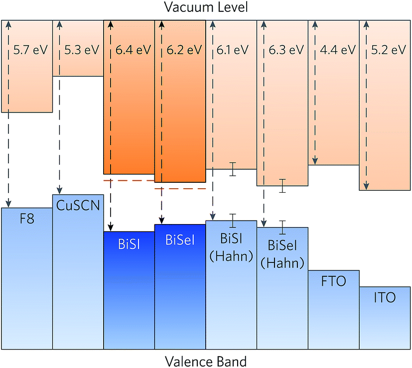 | ||
| Fig. 5 Calculated band alignment of BiSI and BiSeI with a range of hole transporting materials and transparent conducting oxides, taken from experiment.85–90 The CBM alignments from the HSE06 calculated VBM energy levels and extrapolated using the experimental band gaps are shown in dashed red lines. Alignments calculated from experiment by Hahn et al. are also included, with the experimental error indicated.42 | ||
The band alignments for a range of hole transporting materials and n-type transparent conducting oxides are also shown in Fig. 5. Due to the unexpectedly large ionisation potential of BiSI, the materials used in the cells fabricated by Hahn et al., namely p-CuSCN and FTO, result in misalignment of the conduction band minimum against both the hole transporting and transparent conducting oxide layers.42 When the calculated valence band maximum alignment of BiSI is combined with the experimental band gap, the valence band maximum of p-CuSCN occurs only ∼0.4 eV below the conduction band minimum of BiSI, severely limiting the voltage at open-circuit.85,86 As such, a hole transporting material with a lower valence band maximum, such as poly(fluorene-2,7-diyl) (F8, IP = 5.7 eV),87 is necessary to maximise the open-circuit voltage of the p–n junction and increase device efficiencies. Conversely, the conduction band minimum of FTO (EA ≃ 4.4 eV)88 occurs above the conduction band minimum of BiSI and BiSeI (EA = 4.9 eV and 5.0 eV, respectively), indicating that there will be poor transfer of electrons to the window layer. A material with a larger electron affinity, such as indium tin oxide (ITO, EA ≃ 5.2 eV)89,90 or lead-doped tin oxide (Pb:SnO2, EA ≃ 5.0 eV),95 should therefore be used to promote efficient transport of photo-generated electrons. We note that our analysis only takes into account the fundamental band alignments and does include any effects arising from interfacial strain or chemical interactions occurring at the interface. Nonetheless, the need for developing new contact materials is clear.
Conclusions
We have demonstrated, using first-principles relativistic electronic structure theory, that BiSI and BiSeI possess suitable electronic structures for solar energy applications, with only a small difference between the direct and indirect band gaps and low electron effective masses in the direction along the BiChI chains. Additionally, the presence of antibonding states at the top of the valence band, coupled with high dielectric constants, is expected to provide a high level of defect tolerance ideal for efficient solar absorbers. Previously, devices containing these materials have performed poorly, this is in part due to the 1D nature of the ribbon structure, which should be vertically oriented on the device in order to provide clear conduction pathways. Additionally, the large electron affinity of these materials (>4.9 eV) results in band misalignments with commonly used electron transport materials and, as such, we have suggested alternatives that are likely to increase device efficiencies.Acknowledgements
This work made use of the ARCHER UK National Supercomputing Service (http://www.archer.ac.uk), via our membership of the UK's HEC Materials Chemistry Consortium, which is funded by EPSRC (EP/L000202) and the UCL Legion HPC Facility (Legion@UCL). The work at UCL was supported by EPSRC (EP/N01572X/1). The work at Bath was supported by the ERC (Grant no. 277757) and the EPSRC (Grant no. EP/K016288/1, EP/L017792/1 and EP/M009580/1). DOS acknowledges support from the SUPERSOLAR Solar Energy Hub (EP/J017361/1) for the provision of a flexible funding call award. AMG acknowledges Diamond Light Source for the co-sponsorship of a studentship on the EPSRC Centre for Doctoral Training in Molecular Modelling and Materials Science (EP/L015862/1).References
- W. Hermann, Quantifying global exergy resources, Energy, 2006, 31, 1685–1702 CrossRef CAS.
- L. M. Peter, Towards Sustainable Photovoltaics: The Search for New Materials, Philos. Trans. R. Soc., A, 2011, 369, 1840–1856 CrossRef CAS PubMed.
- S. Hegedus, Thin Film Solar Modules: The Low Cost, High Throughput and Versatile Alternative to Si Wafers, Progress in Photovoltaics: Research and Applications, 2006, 14, 393–411 CrossRef CAS.
- J. Peng, L. Lu and H. Yang, Review On Life Cycle Assessment of Energy Payback and Greenhouse Gas Emission of Solar Photovoltaic Systems, Renewable Sustainable Energy Rev., 2013, 19, 255–274 CrossRef CAS.
- P. Jackson, D. Hariskos, E. Lotter, S. Paetel, R. Wuerz, R. Menner, W. Wischmann and M. Powalla, New World Record Efficiency for Cu(In,Ga)Se2 Thin-Film Solar Cells Beyond 20%, Progress in Photovoltaics: Research and Applications, 2011, 19, 894–897 CrossRef CAS.
- M. A. Green, K. Emery, Y. Hishikawa, W. Warta and E. D. Dunlop, Solar Cell Efficiency Tables (Version 46), Progress in Photovoltaics: Research and Applications, 2015, 23, 805–812 CrossRef.
- B. O'Neill, Indium market forces, a commercial perspective. 2010 35th IEEE Photovoltaic Specialists Conference, 2010, pp. 000556–000559 Search PubMed.
- D. J. Temple, A. B. Kehoe, J. P. Allen, G. W. Watson and D. O. Scanlon, Geometry, Electronic Structure, and Bonding in CuMCh2 (M= Sb, Bi; Ch= S, Se): Alternative Solar Cell Absorber Materials?, J. Mater. Chem. C, 2012, 116, 7334–7340 CAS.
- A. B. Kehoe, D. J. Temple, G. W. Watson and D. O. Scanlon, Cu3MCh3 (M= Sb, Bi; Ch= S, Se) As Candidate Solar Cell Absorbers: Insights From Theory, Phys. Chem. Chem. Phys., 2013, 15, 15477–15484 RSC.
- N. Feldberg, B. Keen, J. Aldous, D. Scanlon, P. Stampe, R. Kennedy, R. Reeves, T. Veal and S. Durbin, ZnSnN2: A New Earth-Abundant Element Semiconductor for Solar Cells. Photovoltaic Specialists Conference (PVSC), 2012 38th IEEE, 2012, pp. 002524–002527 Search PubMed.
- D. O. Scanlon and A. Walsh, Bandgap Engineering of ZnSnP2 for High-Efficiency Solar Cells, Appl. Phys. Lett., 2012, 100, 251911 CrossRef.
- M. a. Green, A. Ho-Baillie and H. J. Snaith, The Emergence of Perovskite Solar Cells, Nat. Photonics, 2014, 8, 506–514 CrossRef CAS.
- M. Grätzel, The Light and Shade of Perovskite Solar Cells, Nat. Mater., 2014, 13, 838–842 CrossRef PubMed.
- A. T. Barrows, A. J. Pearson, C. K. Kwak, A. D. F. Dunbar, A. R. Buckley and D. G. Lidzey, Efficient Planar Heterojunction Mixed-halide Perovskite Solar Cells Deposited via Spray-Deposition, Energy Environ. Sci., 2014, 7, 2944 CAS.
- D. S. Bhachu, D. O. Scanlon, E. J. Saban, H. Bronstein, I. P. Parkin, C. J. Carmalt and R. G. Palgrave, Scalable Route to CH3NH3PbI3 Perovskite Thin Films by Aerosol Assisted Chemical Vapour Deposition, J. Mater. Chem. A, 2015, 3, 9071–9073 CAS.
- G. Hodes and D. Cahen, Photovoltaics Perovskite Cells Roll Forward, Nat. Photonics, 2014, 8, 87–88 CrossRef CAS.
- W. Wang, M. T. Winkler, O. Gunawan, T. Gokmen, T. K. Todorov, Y. Zhu and D. B. Mitzi, Device Characteristics of CZTSSe Thin-Film Solar Cells with 12.6% Efficiency, Adv. Energy Mater., 2014, 4, 1301465 Search PubMed.
- R. Komiya, A. Fukui, N. Murofushi, N. Koide, R. Yamanaka and H. Katayama, Improvement of the Conversion Efficiency of a Monolithic Type Dyesensitized Solar Cell Module. Technical Digest of the 21st International Photovoltaic Science and Engineering Conference, 2C-5O-08, Fukuoka, Japan, 2011 Search PubMed.
- H.-S. Kim, S. H. Im and N.-G. Park, Organolead Halide Perovskite: New Horizons in Solar Cell Research, J. Mater. Chem. C, 2014, 118, 5615–5625 CAS.
- W. S. Yang, J. H. Noh, N. J. Jeon, Y. C. Kim, S. Ryu, J. Seo and S. I. Seok, High-Performance Photovoltaic Perovskite Layers Fabricated Through Intramolecular Exchange, Science, 2015, 348, 1234–1237 CrossRef CAS PubMed.
- S. Guarnera, A. Abate, W. Zhang, J. M. Foster, G. Richardson, A. Petrozza and H. J. Snaith, Improving the Long-Term Stability of Perovskite Solar Cells with a Porous Al2O3 Buffer Layer, J. Phys. Chem. Lett., 2015, 6, 432–437 CrossRef CAS PubMed.
- G. Niu, X. Guo and L. Wang, Review of Recent Progress in Chemical Stability of Perovskite Solar Cells, J. Mater. Chem. A, 2015, 3, 8970–8980 CAS.
- A. Pisoni, J. Jaćimović, O. S. Barišić, M. Spina, R. Gaál, L. Forró and E. Horváth, Ultra-Low Thermal Conductivity in Organic–Inorganic Hybrid Perovskite CH3NH3PbI3, J. Phys. Chem. Lett., 2014, 5, 2488–2492 CrossRef CAS PubMed.
- R. E. Brandt, V. Stevanović, D. S. Ginley and T. Buonassisi, Identifying Defect-Tolerant Semiconductors with High Minority-Carrier Lifetimes: Beyond Hybrid Lead Halide Perovskites, MRS Commun., 2015, 5, 1–11 CrossRef.
- A. J. Lehner, D. H. Fabini, H. A. Evans, C.-A. Hébert, S. R. Smock, J. Hu, H. Wang, J. W. Zwanziger, M. L. Chabinyc and R. Seshadri, Crystal and Electronic Structures of Complex Bismuth Iodides A3Bi2I9 (A= K, Rb, Cs) Related to Perovskite: Aiding the Rational Design of Photovoltaics, Chem. Mater., 2015, 27, 7137–7148 CrossRef CAS.
- R. E. Brandt, R. C. Kurchin, R. L. Hoye, J. R. Poindexter, M. W. B. Wilson, S. Sulekar, F. Lenahan, P. X. Yen, V. Stevanovic, J. C. Nino, M. G. Bawendi and T. Buonassisi, Investigation of Bismuth Triiodide (BiI3) for Photovoltaic Applications, J. Phys. Chem. Lett., 2015, 6, 4297–4302 CrossRef CAS PubMed.
- A. Walsh, D. J. Payne, R. G. Egdell and G. W. Watson, Stereochemistry of Post-Transition Metal Oxides: Revision of the Classical Lone Pair Model, Chem. Soc. Rev., 2011, 40, 4455–4463 RSC.
- L. M. Wu, X. T. Wu and L. Chen, Structural Overview and Structure–Property Relationships of Iodoplumbate and Iodobismuthate, Coord. Chem. Rev., 2009, 253, 2787–2804 CrossRef CAS.
- D. B. Mitzi and P. Brock, Structure and Optical Properties of Several Organic–Inorganic Hybrids Containing Corner-Sharing Chains of Bismuth Iodide Octahedra, Inorg. Chem., 2001, 40, 2096–2104 CrossRef CAS PubMed.
- F. Demartin, C. Gramaccioli and I. Campostrini, Demicheleite-(I), BiSI, a New Mineral from La Fossa Crater, Vulcano, Aeolian Islands, Italy, Mineral. Mag., 2010, 74, 141–145 CrossRef CAS.
- B. Frit and J. Mercurio, The Crystal Chemistry and Dielectric Properties of the Aurivillius Family of Complex Bismuth Oxides with Perovskite-Like Layered Structures, J. Alloys Compd., 1992, 188, 27–35 CrossRef CAS.
- P. Umari, E. Mosconi and F. De Angelis, Relativistic GW Calculations On CH3NH3PbI3 and CH3NH3SnI3 Perovskites For Solar Cell Applications, Sci. Rep., 2014, 4, 4467 Search PubMed.
- A. Ganose, C. N. Savory and D. O. Scanlon, (CH3NH3)2Pb(SCN)2I2: A More Stable Structural Motif for Hybrid Halide Photovoltaics?, J. Phys. Chem. Lett., 2015, 6, 4594–4598 CrossRef CAS PubMed.
- F. Brivio, K. T. Butler, A. Walsh and M. Van Schilfgaarde, Relativistic Quasiparticle Self-Consistent Electronic Structure of Hybrid Halide Perovskite Photovoltaic Absorbers, Phys. Rev. B: Condens. Matter Mater. Phys., 2014, 89, 155204 CrossRef.
- A. Slikkerveer and F. A. de Wolff, Pharmacokinetics and Toxicity of Bismuth Compounds, Med. Toxicol. Adverse Drug Exper., 1989, 4, 303–323 CrossRef CAS.
- W. Serfontein and R. Mekel, Bismuth Toxicity in Man II. Review of Bismuth Blood and Urine Levels in Patients After Administration of Therapeutic Bismuth Formulations in Relation to the Problem of Bismuth Toxicity in Man, Res. Commun. Chem. Pathol. Pharmacol., 1979, 26, 391–411 CAS.
- A. J. Lehner, H. Wang, D. H. Fabini, C. D. Liman, C.-A. Hébert, E. E. Perry, M. Wang, G. C. Bazan, M. L. Chabinyc and R. Seshadri, Electronic Structure and Photovoltaic Application of BiI3, Appl. Phys. Lett., 2015, 107, 131109 CrossRef.
- B.-W. Park, B. Philippe, X. Zhang, H. Rensmo, G. Boschloo and E. M. Johansson, Bismuth Based Hybrid Perovskites A3Bi2I9 (A: Methylammonium or Cesium) for Solar Cell Application, Adv. Mater., 2015, 27, 6806–6813 CrossRef CAS PubMed.
- S. Sun; S. Tominaka; J.-H. Lee; F. Xie; P. D. Bristowe; A. K. Cheetham. Synthesis, Crystal Structure and Properties of a Perovskite-Related Bismuth Phase, (NH4)3Bi2I9, 2015, arXiv preprint arXiv:1509.08126.
- T. P. Braun and F. J. DiSalvo, Bismuth Selenide Iodide, Acta Crystallogr., Sect. C: Cryst. Struct. Commun., 2000, 56, 1–2 Search PubMed.
- Y. Zhou, L. Wang, S. Chen, S. Qin, X. Liu, J. Chen, D.-J. Xue, M. Luo, Y. Cao and Y. Cheng, Thin-Film Sb2Se3 Photovoltaics with Oriented One-Dimensional Ribbons and Benign Grain Boundaries, Nat. Photonics, 2015, 9, 409–415 CrossRef CAS.
- N. T. Hahn, A. J. Rettie, S. K. Beal, R. R. Fullon and C. B. Mullins, n-BiSI Thin Films: Selenium Doping and Solar Cell Behavior, J. Mater. Chem. C, 2012, 116, 24878–24886 CAS.
- N. T. Hahn, J. L. Self and C. B. Mullins, BiSI Micro-Rod Thin Films: Efficient Solar Absorber Electrodes?, J. Phys. Chem. Lett., 2012, 3, 1571–1576 CrossRef CAS PubMed.
- J. M. Frost, K. T. Butler, F. Brivio, C. H. Hendon, M. Van Schilfgaarde and A. Walsh, Atomistic Origins of High-Performance in Hybrid Halide Perovskite Solar Cells, Nano Lett., 2014, 14, 2584–2590 CrossRef CAS PubMed.
- A. Walsh, Principles of Chemical Bonding and Band Gap Engineering in Hybrid Organic–Inorganic Halide Perovskites, J. Mater. Chem. C, 2015, 119, 5755–5760 CAS.
- G. Kresse and J. Hafner, Ab Initio Molecular Dynamics for Liquid Metals, Phys. Rev. B: Condens. Matter Mater. Phys., 1993, 47, 558–561 CrossRef CAS.
- G. Kresse and J. Hafner, Ab Initio Molecular-Dynamics Simulation of the Liquid-Metal Amorphous-Semiconductor Transition in Germanium, Phys. Rev. B: Condens. Matter Mater. Phys., 1994, 49, 14251–14269 CrossRef CAS.
- G. Kresse and J. Furthmüller, Efficient Iterative Schemes for Ab Initio Total-Energy Calculations Using a Plane-Wave Basis Set, Phys. Rev. B: Condens. Matter Mater. Phys., 1996, 54, 11169–11186 CrossRef CAS.
- G. Kresse and J. Furthmüller, Efficiency of Ab Initio Total Energy Calculations for Metals and Semiconductors Using a Plane Wave Basis Set, Comput. Mater. Sci., 1996, 6, 15 CrossRef CAS.
- G. Kresse, From Ultrasoft Pseudopotentials to the Projector Augmented-Wave Method, Phys. Rev. B: Condens. Matter Mater. Phys., 1999, 59, 1758–1775 CrossRef CAS.
- J. P. Perdew, K. Burke and M. Ernzerhof, Generalized Gradient Approximation Made Simple, Phys. Rev. Lett., 1996, 77, 3865–3868 CrossRef CAS PubMed.
- J. P. Perdew, A. Ruzsinszky, G. I. Csonka, O. A. Vydrov, G. E. Scuseria, L. A. Constantin, X. Zhou and K. Burke, Restoring the Density-Gradient Expansion for Exchange in Solids and Surfaces, Phys. Rev. Lett., 2008, 100, 136406 CrossRef PubMed.
- S. Grimme, Accurate Description of van der Waals Complexes by Density Functional Theory Including Empirical Corrections, J. Comput. Chem., 2004, 25, 1463–1473 CrossRef CAS PubMed.
- T. Björkman, van der Waals Density Functional for Solids, Phys. Rev. B: Condens. Matter Mater. Phys., 2012, 86, 165109 CrossRef.
- A. V. Krukau, O. A. Vydrov, A. F. Izmaylov and G. E. Scuseria, Influence of the Exchange Screening Parameter on the Performance of Screened Hybrid Functionals, J. Chem. Phys., 2006, 125, 224106 CrossRef PubMed.
- K. T. Butler, J. M. Frost and A. Walsh, Ferroelectric Materials for Solar Energy Conversion: Photoferroics Revisited, Energy Environ. Sci., 2015, 8, 838–848 CAS.
- Y.-Y. Sun, J. Shi, J. Lian, W. Gao, M. L. Agiorgousis, P. Zhang and S. Zhang, Discovering Lead-Free Perovskite Solar Materials with a Split-Anion Approach, Nanoscale, 2015 10.1039/C5NR04310G.
- R. Dronskowski and P. E. Bloechl, Crystal Orbital Hamilton Populations (COHP): Energy-Resolved Visualization of Chemical Bonding in Solids Based on Density-Functional Calculations, J. Phys. Chem., 1993, 97, 8617–8624 CrossRef CAS.
- S. Maintz, V. L. Deringer, A. L. Tchougréeff and R. Dronskowski, Analytic Projection from Plane-Wave and Paw Wavefunctions and Application to Chemical-Bonding Analysis in Solids, J. Comput. Chem., 2013, 34, 2557–2567 CrossRef CAS PubMed.
- R. X. Yang, K. T. Butler and A. Walsh, Assessment of Hybrid Organic–Inorganic Antimony Sulfides for Earth-Abundant Photovoltaic Applications, J. Phys. Chem. Lett., 2015, 6, 5009–5014 CrossRef CAS PubMed.
- A. Walsh and K. T. Butler, Prediction of Electron Energies in Metal Oxides, Acc. Chem. Res., 2013, 47, 364–372 CrossRef PubMed.
- L. A. Burton and A. Walsh, Band Alignment in SnS Thin-Film Solar Cells: Possible Origin of the Low Conversion Efficiency, Appl. Phys. Lett., 2013, 102, 132111 CrossRef.
- J. Brgoch, A. J. Lehner, M. Chabinyc and R. Seshadri, Ab Initio Calculations of Band Gaps and Absolute Band Positions of Polymorphs of RbPbI3 and CsPbI3: Implications for Main-Group Halide Perovskite Photovoltaics, J. Mater. Chem. C, 2014, 118, 27721–27727 CAS.
- https://www.github.com/SMTG-UCL/BiChI, accessed: 2015-11-12.
- S.-A. Park, M.-Y. Kim, J.-Y. Lim, B.-S. Park, J.-D. Koh and W.-T. Kim, Optical Properties of Undoped and V-Doped VA-VIA-VIIA Single Crystals, Phys. Status Solidi B, 1995, 187, 253–260 CrossRef CAS.
- S.-C. Hyun, Y.-G. Kim, M.-Y. Kim, J.-D. Koh, B.-S. Park and W.-T. Kim, Optical Properties of Undoped and Chromium-Doped VA-VIA-VIIA Single Crystals, J. Mater. Sci., 1995, 30, 6113–6117 CrossRef CAS.
- J. Dunitz and L. Orgel, Stereochemistry of Ionic Solids, Adv. Inorg. Chem. Radiochem., 1960, 2, 1–60 CrossRef CAS.
- L. Orgel, 769. The Stereochemistry of B Subgroup Metals. Part II. The Inert Pair, J. Chem. Soc., 1959, 3815–3819 RSC.
- A. Walsh and G. W. Watson, The Origin of the Stereochemically Active Pb(II) Lone Pair: DFT Calculations on PbO and PbS, J. Solid State Chem., 2005, 178, 1422–1428 CrossRef CAS.
- S. Zhang, S.-H. Wei, A. Zunger and H. Katayama-Yoshida, Defect Physics of the CuInSe2 Chalcopyrite Semiconductor, Phys. Rev. B: Condens. Matter Mater. Phys., 1998, 57, 9642 CrossRef CAS.
- A. Zakutayev, C. M. Caskey, A. N. Fioretti, D. S. Ginley, J. Vidal, V. Stevanovic, E. Tea and S. Lany, Defect Tolerant Semiconductors for Solar Energy Conversion, J. Phys. Chem. Lett., 2014, 5, 1117–1125 CrossRef CAS PubMed.
- A. Walsh and G. W. Watson, Influence of the Anion On Lone Pair Formation in Sn(II) Monochalcogenides: A DFT Study, J. Phys. Chem. B, 2005, 109, 18868–18875 CrossRef CAS PubMed.
- A. Walsh, G. W. Watson, D. J. Payne, R. G. Edgell, J. Guo, P.-A. Glans, T. Learmonth and K. E. Smith, Electronic Structure of the α and δ Phases of Bi2O3: A Combined Ab Initio and X-ray Spectroscopy Study, Phys. Rev. B: Condens. Matter Mater. Phys., 2006, 73, 235104 CrossRef.
- U. Waghmare, N. Spaldin, H. Kandpal and R. Seshadri, First-Principles Indicators of Metallicity and Cation Off-Centricity in the IV–VI Rocksalt Chalcogenides of Divalent Ge, Sn, and Pb, Phys. Rev. B: Condens. Matter Mater. Phys., 2003, 67, 125111 CrossRef.
- A. Walsh and G. W. Watson, Polymorphism in Bismuth Stannate: A First-Principles Study, Chem. Mater., 2007, 19, 5158–5164 CrossRef CAS.
- C. Svensson, The Crystal Structure of Orthorhombic Antimony Trioxide, Sb2O3, Acta Crystallogr., Sect. B: Struct. Sci., 1974, 30, 458–461 CrossRef CAS.
- O. Micic, Z. Li, G. Mills, J. Sullivan and D. Meisel, Formation of Small Particles of Lead Iodide, Mercuric Iodide, and Bismuth Iodide Layered Semiconductors, J. Phys. Chem., 1987, 91, 6221–6229 CrossRef CAS.
- D. Guo, C. Hu and C. Zhang, First-Principles Study on Doping and Temperature Dependence of Thermoelectric Property of Bi2S3 Thermoelectric Material, Mater. Res. Bull., 2013, 48, 1984–1988 CrossRef CAS.
- A. Walsh, D. O. Scanlon, S. Chen, X. Gong and S.-H. Wei, Self-Regulation Mechanism for Charged Point Defects in Hybrid Halide Perovskites, Angew. Chem., 2015, 127, 1811–1814 CrossRef.
- R. H. Bube, Photoelectronic Properties of Semiconductors, Cambridge University Press, 1992 Search PubMed.
- M. Cardona and Y. Y. Peter, Fundamentals of Semiconductors, Springer, 2005 Search PubMed.
- J. M. Frost, K. T. Butler and A. Walsh, Molecular Ferroelectric Contributions to Anomalous Hysteresis in Hybrid Perovskite Solar Cells, APL Mater., 2014, 2, 081506 CrossRef.
- P. Fernandes, P. Salomé and A. Da Cunha, Precursors' Order Effect on the Properties of Sulfurized Cu2ZnSnS4 Thin Films, Semicond. Sci. Technol., 2009, 24, 105013 CrossRef.
- G. Allan, C. Delerue, M. Lannoo and E. Martin, Hydrogenic Impurity Levels, Dielectric Constant, and Coulomb Charging Effects in Silicon Crystallites, Phys. Rev. B: Condens. Matter Mater. Phys., 1995, 52, 11982 CrossRef CAS.
- P. P. Boix, G. Larramona, A. Jacob, B. Delatouche, I. Mora-Seró and J. Bisquert, Hole Transport and Recombination in All-Solid Sb2S3-Sensitized TiO2 Solar Cells Using CuSCN As Hole Transporter, J. Mater. Chem. C, 2011, 116, 1579–1587 Search PubMed.
- X. Chao, C. Lei and Y. Hongchun, Study on the Synthesis, Characterization of p-CuSCN/n-Si Heterojunction, Open Mater. Sci. J., 2013, 7, 29–32 CrossRef.
- M. Inbasekaran, E. Woo, W. Wu, M. Bernius and L. Wujkowski, Fluorene Homopolymers and Copolymers, Synth. Met., 2000, 111, 397–401 CrossRef.
- M. Helander, M. Greiner, Z. Wang, W. Tang and Z. Lu, Work Function of Fluorine Doped Tin Oxide, J. Vac. Sci. Technol., A, 2011, 29, 011019 Search PubMed.
- C. Dong, W. Yu, M. Xu, J. Cao, C. Chen, W. Yu and Y. Wang, Valence Band Offset of Cu2O/In2O3 Heterojunction Determined By X-Ray Photoelectron Spectroscopy, J. Appl. Phys., 2011, 110, 073712 CrossRef.
- B. Höffling, A. Schleife, C. Rödl and F. Bechstedt, Band Discontinuities at Si–TCO Interfaces from Quasiparticle Calculations: Comparison of Two Alignment Approaches, Phys. Rev. B: Condens. Matter Mater. Phys., 2012, 85, 035305 CrossRef.
- W. Jaegermann, A. Klein and T. Mayer, Interface Engineering of Inorganic Thin-Film Solar Cells–Materials-Science Challenges for Advanced Physical Concepts, Adv. Mater., 2009, 21, 4196–4206 CrossRef CAS.
- Z. Chen, W. Peng, K. Zhang, J. Zhang, X. Yang, Y. Numata and L. Han, Band Alignment By Ternary Crystalline Potential-Tuning Interlayer for Efficient Electron Injection in Quantum Dot-Sensitized Solar Cells, J. Mater. Chem. A, 2014, 2, 7004–7014 CAS.
- B. I. MacDonald, A. Martucci, S. Rubanov, S. E. Watkins, P. Mulvaney and J. J. Jasieniak, Layer-by-Layer Assembly of Sintered CdSexTe1−x Nanocrystal Solar Cells, ACS Nano, 2012, 6, 5995–6004 CrossRef CAS PubMed.
- S. Chen, A. Walsh, J.-H. Yang, X. Gong, L. Sun, P.-X. Yang, J.-H. Chu and S.-H. Wei, Compositional Dependence of Structural and Electronic Properties Of Cu2ZnSn(S,Se)4 Alloys for Thin Film Solar Cells, Phys. Rev. B: Condens. Matter Mater. Phys., 2011, 83, 125201 CrossRef.
- A. M. Ganose and D. O. Scanlon, Band Gap and Work Function Tailoring of SnO2 for Improved Transparent Conducting Ability in Photovoltaics, J. Mater. Chem. C, 2016 10.1039/C5TC04089B.
Footnote |
| † Electronic supplementary information (ESI) available. See DOI: 10.1039/c5ta09612j |
| This journal is © The Royal Society of Chemistry 2016 |