
 Open Access Article
 This Open Access Article is licensed under a Creative Commons Attribution-Non Commercial 3.0 Unported Licence
Utilizing modeling, experiments, and statistics for the analysis of water-splitting photoelectrodes†
Yannick K.
Gaudy
and
Sophia
Haussener
*
Institute of Mechanical Engineering, École Polytechnique Fédérale de Lausanne, 1015 Lausanne, Switzerland. E-mail: sophia.haussener@epfl.ch; Tel: +41 21 693 3878
First published on 22nd December 2015
Abstract
A multi-physics model of a planar water-splitting photoelectrode was developed, validated, and used to identify and quantify the most significant materials-related bottlenecks in photoelectrochemical device performance. The model accounted for electromagnetic wave propagation within the electrolyte and semiconductor, and for charge carrier transport within the semiconductor and at the semiconductor–electrolyte interface. Interface states at the semiconductor–electrolyte interface were considered using an extended Schottky contact model. The numerical model was validated with current–voltage measurements using an n-type GaN photoanode immersed in 1 M H2SO4. Numerical design of experiments and parametric analysis were conducted using the validated model in order to identify and optimize the key factors for water-splitting photoelectrodes. The methodology, developed using an experimentally-validated numerical model coupled to statistical analysis, provides a general approach to identify and quantify the main material challenges and design considerations in working PEC devices. In the case of n-type GaN, the surface recombination, flatband potential, and doping concentration were identified as the most significant parameters for the photocurrent density.
1. Introduction
Photoelectrochemical (PEC) water-splitting devices require light absorbers, charge generators and separators, selective electrocatalysts, ion conducting electrolytes, and product separating semi-permeable membranes. Different approaches to integrated PEC water-splitting devices have been investigated.1–3 Their key difference is the use of a solid–liquid junction (PEC cell), a solid–solid junction (PV cell), or combinations thereof, for charge separation.4,5 PV cell-based approaches allow for a separate optimization of the semiconductor and the electrolyte but suffer from more complex and expensive manufacturing and, usually, stability issues of the PV cell in the electrolyte. PEC cell-based approaches have the potential to be cheaper and provide tunable interface properties, but don't allow for separate treatment of the semiconductor, electrolyte, and sometimes the catalysts. The semiconductor–electrolyte interface is at the core of PEC water-splitting devices performance6 and therefore requires special focus and investigation.Research focusing on the energy and charge transfer phenomena at the illuminated semiconductor–liquid interface was pioneered by Marcus and Gerischer, and has considerably progressed over the decades.6–13 Electrochemistry at the semiconductor–liquid interface is often discussed in terms of the Marcus–Gerischer model10 which refers to ideal direct charge transfer. Nevertheless, deviations from the ideal charge transfer are observed in the presence of interface states as is observed for many semiconductor–electrolyte interfaces. Recently, numerical modelling of the charge transfer at the semiconductor–electrolyte interface and its coupling to multiphysical heat, mass, and charge transport phenomena in a complete PEC device has become of interest as it can provide insight into the coupled physical phenomena inaccessible to experiments. Models of charge transport in the semiconductor have enhanced the understanding of the energy band dynamics of photoabsorbers in direct contact with an electrolyte,14 insight that can only be captured by numerical calculations. A 1-dimensional model of a PEC water-splitting device integrating light absorption, charge transport in the semiconductor, charge transfer to the metallic catalyst, and charge transport in the electrolyte has quantified the dependency of the device performance on the choice of the light absorber.15 Theory and numerical modeling of charge transfer at semiconductor–catalyst interfaces for solar water-splitting have been developed to describe current–voltage behavior of semiconductor–catalyst–solution systems with metallic, adaptive, and molecular catalysts.13 These models do not simultaneously study electromagnetic wave propagation and charge transport in the semiconductor and/or do not consider all types of relevant recombination phenomena, such as surface recombination, which can be a major loss at semiconductor–electrolyte interfaces.13,16,17 A detailed quantification and decoupling of the influence of the photon absorption, charge generation, charge transport and recombination, and interface transport and recombination phenomena is missing.
In this work, we uniquely combine numerical modeling, experimental measurements, and statistical analysis for the development of an accurate water-splitting photoelectrode performance model, identification and quantification of the key performance parameters, and subsequent proposition of material and device optimization. First, we introduce the numerical model, which combines electromagnetic wave propagation, charge generation and transport in the semiconductor, and charge transfer across the catalytically active semiconductor–electrolyte interface. The numerical model is then applied to a model system composed of a planar gallium nitride photoanode and platinum wire cathode immersed in 1 M sulfuric acid. The numerical model is completed with experimental investigations to determine missing material parameters of gallium nitride. The numerical model is subsequently experimentally validated using linear sweep voltammetry measurements. Statistical methods are used in combination with the validated model to identify the most important material and interface properties. Finally, parametric analyses are used to optimize identified key performance parameters of the water-splitting photoelectrode.
2. Governing equations and methodology
2.1. Model domain and assumptions
The modeled water-splitting photoelectrode consists of a planar photoanode (GaN) electrically connected to a wired counter electrode (Pt), both immersed in an electrolyte (sulfuric acid). The detailed arrangement of the planar photoelectrode, including substrate and highly-doped conduction layers, is depicted in Fig. 1a.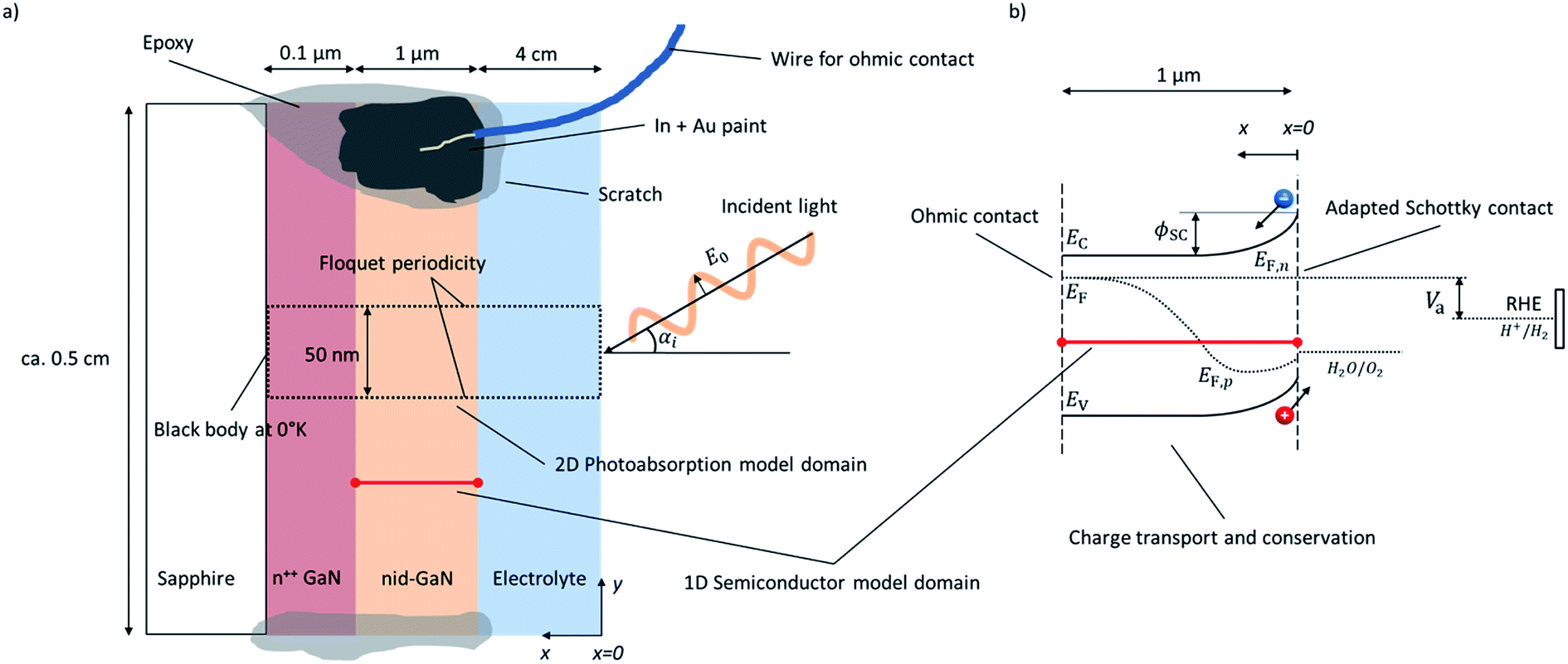 | ||
| Fig. 1 (a) Scheme of the model domain (not to scale) of the photoanode (GaN) immersed in electrolyte including the 2D EMW propagation model domain (dotted) and boundary conditions, and the 1D semiconductor model domain (red line). (b) Detailed 1D semiconductor model domain and boundary conditions. EC and EV are the conduction and valence band potential levels, respectively. ϕsc is the space charge layer potential, EF, EF,n and EF,p are the Fermi level, the electron and hole quasi-Fermi level potentials, respectively. Va is the applied potential versus the reversible hydrogen electrode. | ||
Electromagnetic wave (EMW) propagation is calculated in all components of the device (electrolyte and semiconductor), assuming solar irradiation at the top of the electrolyte and absorption at the back contact of the photoanode. The 2D model domain and its boundaries are indicated by a dotted frame in Fig. 1a. The radiation model attempts to be applicable to any type of photoelectrode or PEC device justifying the choice of the advanced light propagation model. The typically applied Beer–Lambert's law13–15 limits the calculation of the charge generation rate to planar, homogeneous photoelectrodes, while detailed EMW propagation calculations provide solutions to the investigation and optimization of morphologically-complex, nano-structured, heterogeneous, or multi-component water-splitting photoelectrodes. Similarly, ray-tracing methods are also limited to cases where geometrical optics are valid, i.e. the thickness of the absorber is larger than the light wavelength.18
Charge transport and conservation is solved only in the semiconductor component, utilizing dedicated boundary conditions to ensure the physical coupling to the counter electrode and the electrolyte; the front semiconductor domain boundary consists of a semiconductor–electrolyte interface, and the back semiconductor domain interface consists of a semiconductor–metal ohmic contact. The 1D model domain and its boundaries are indicated by a red line in Fig. 1. The governing equations of chemical species transport and reactions in the electrolyte are well known19–21 and have been previously studied.22 Detailed analysis of the charge and species transport in the electrolyte was not considered in our study, assuming a highly conducting electrolyte with an excess availability of ions, no significant species concentration variations, and no mass transport limitations. Dissolved and gas-phase products such as oxygen and hydrogen were assumed to be quickly evacuated from the semiconductor–electrolyte interface. Generally, the electrolyte was assumed to be well stirred and purged. Flatband potentials were assumed to be unaffected by species adsorption at the semiconductor surface.
Our numerical model consists of two parts as depicted in Fig. 1: (i) a 2D model of the EMW propagation in the electrolyte and semiconductor that allows determination of the generation rate of electron–hole pairs in the semiconductor, and (ii) a 1D model of the charge transport and conservation in the semiconductor that allows determination of charge carrier concentrations, band positions, recombination rates, (photo)current, and potentials. The EMW propagation in 2D was developed to provide a general model enabling future study on more complex device structures. The advanced multi-dimensional EMW did not lead to significant additional computational expenses, as the electron–hole-pair generation rate was calculated only one time assuming that the complex refractive index was independent of the other semiconductor material properties. The 1D semiconductor model allowed for a computationally effective calculation and exploration of the material parameters of the semiconductor. Physical effects on charge transport due to multi-dimensionality of the sample were neglected and irrelevant for the planar sample with the highly conducting current collector.
The EMW propagation model assumed materials with a relative magnetic permeability of 1 and an electrical conductivity of zero. The various components were assumed rigid, homogeneous, and isotropic. Only steady state operation was considered, and time dependent effects such as photocorrosion were not considered.
Photoabsorption. The location-dependent charge carrier generation rate is calculated by solving the Maxwell's curl equations for each spectral band considered and the complex refractive index, ñ(ω) = n(ω) − ik(ω), as relevant material property,23
| ∇ × (∇ × E(x,ω)) − k02ñ(ω)2E(x,ω) = 0. | (1) |
The optical power absorbed per unit volume is calculated from the electric field and the imaginary part of the complex permittivity,
 | (2) |
 | (3) |
Charge transport and conservation. The static behavior of the charge carriers in the semiconductor is calculated by solving Poisson's equation,24
| ∇·(ε0εr∇ϕ) = −ρ = q(n − p + NA− − ND+), | (4) |
The carrier density is given by integrating the product of the Fermi–Dirac distribution and the density of states over all possible states. For a non-degenerated semiconductor, i.e. when the Fermi level is at least 3kBT away from either band edge, the Fermi–Dirac distribution can be replaced by the Maxwell–Boltzmann distribution leading to electron and hole densities given by:24
n = NC![[thin space (1/6-em)]](https://www.rsc.org/images/entities/char_2009.gif) e−(EC−EF)/kB/T, e−(EC−EF)/kB/T, | (5) |
| p = NVe−(EF−EV)/kB/T. | (6) |
The dynamic behavior of the carriers is calculated by solving the drift-diffusion equations for electrons and holes inside the semiconductor,24
| in = μnn∇EC + μnkBT∇n, | (7) |
| ip = μpp∇EV − μpkBT∇p. | (8) |
Isothermal device temperature and thermal equilibrium between the carrier and the lattice were assumed. The conduction band and valence energy levels, EC and EV, are given by EC = Evaccum − qχ and EV = Evaccum − qχ − Eg where Evaccum is the vacuum energy level and χ is the electron affinity. The total current density, itot, is the sum of the electron and hole current densities. The steady state charge conservation is given by,
 | (9) |
| Un/p ≡ RSRHn/p + Rradn/p + RAun/p + Rs,n/p − Gn/p | (10) |
 | (11) |
 is the intrinsic density, and NC and NV the conduction and valence band densities of states, respectively. The electron and hole trap state densities are calculated according to
| n1 = γnnie(Et−Ei)/kB/T, | (12) |
| p1 = γpnie−(Et−Ei)/kB/T, | (13) |
ln(NV/NC). The electron and hole lifetimes in eqn (11) were exchanged by effective electron and hole lifetimes, | (14) |
The direct band-to-band radiative recombination,
| Rradn = Rradp = Cdir(np − γnγpni2), | (15) |
| RAun = RAup = (Caug,nn + Caug,pp)(np − γnγpni2), | (16) |
The boundary conditions for the charge transport were an ohmic contact for the semiconductor–metal interface and an adapted Schottky contact model for the semiconductor–electrolyte interface, both detailed below. The boundary conditions presented here are at steady-state.
Ideal ohmic contact. The ideal ohmic contact (requiring local thermodynamic equilibrium at the contact) assumes that electron and hole quasi-Fermi levels are equal. Under this condition, eqn (4) describes charge neutrality and is used with n0p0 = γnγpni,eff2 to calculate the electron and hole equilibrium densities given as:
 | (17) |
 | (18) |
The current, being conserved under steady-state, is determined by the current at the semiconductor–electrolyte interface, which must be equal to the current at the ohmic contact.
The electrostatic potential boundary condition for the ideal ohmic contact is given by:
| ϕ = Vavs. RHE. | (19) |
Under equilibrium and no applied potential, the potential for the ideal ohmic contact was chosen as zero vs. Reversible Hydrogen Electrode (RHE).
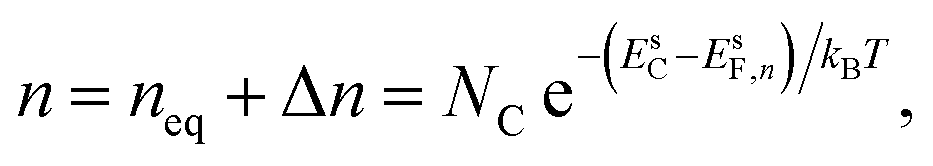
Adapted Schottky contact. An adapted Schottky contact was used for the determination of the current density at the semiconductor–electrolyte interface. Our adapted Schottky contact model accounts for interface states which influence the potential barrier height, ϕB, under dark and illumination, see Fig. 2. In the case of a majority carrier current, it also accounts for the interfacial potential drop distribution between the semiconductor space charge region (SCR) and the Helmholtz layer. Thus, the model enables prediction of band edge pinning or unpinning for majority carrier current.
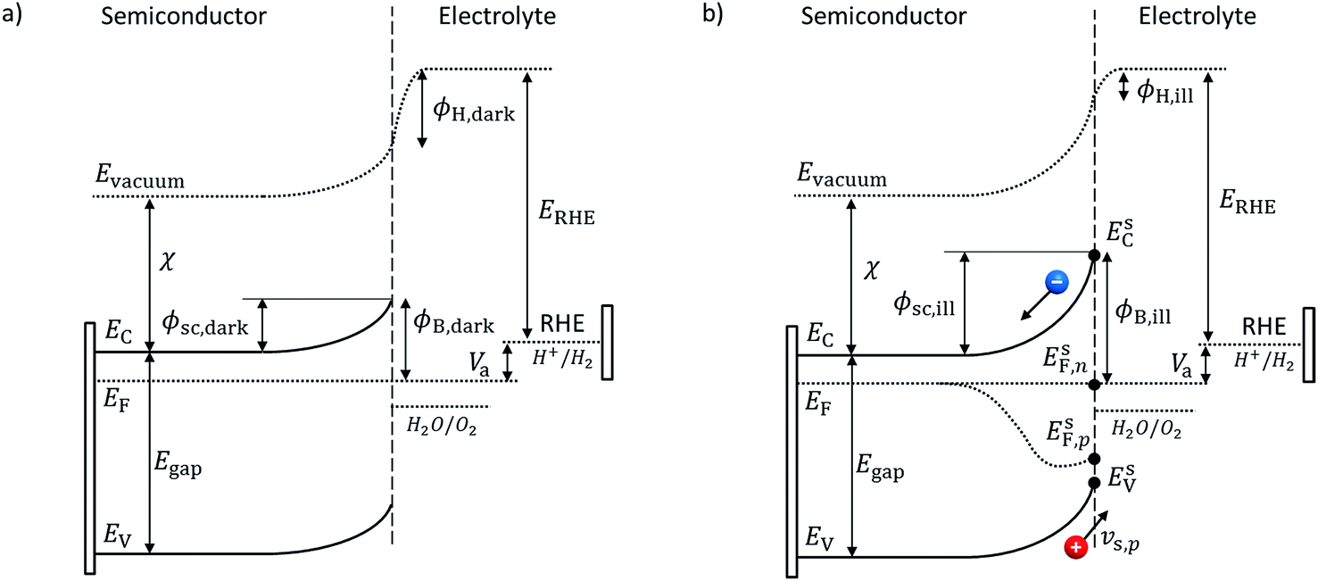 | ||
| Fig. 2 Illustration of a n-type semiconductor–electrolyte interface under dark (a) and illumination (b). The applied potential Va is between the ohmic contact at the back of the photoelectrode and the reference electrode vs. RHE. The subscript “dark” stands for dark condition and “ill” for illuminated condition. The applied potential in this illustration is the same in the dark and illuminated conditions although it does not result in the same SCR. This situation is possible due to different flatband potentials in the dark and under illumination. | ||
An ideal Schottky describes the alignment of the Fermi level of the semiconductor with the dominant redox couple under equilibrium. This alignment provokes a depletion of negative charge (for n-type semiconductor), the SCR, which induces band bending.28 If large concentrations of interface states exist within the bandgap at the surface of the semiconductor–electrolyte interface,29 the Fermi level of the semiconductor might align with the interface states energy level instead and be “pinned” at the interface states' energy level. Upon illumination, the produced minority carriers might not cross the interface and therefore accumulate at the surface or get trapped by interface states30 which results in a change of the SCR potential, and therefore, the Helmholtz layer (HL) (see Fig. 2). This effect is called “unpinning of the band” and can be interpreted as the movement of the band edges. These complex effects were considered in our adapted Schottky contact by adapting the barrier height, ϕB, of the semiconductor SCR according to the flatband potential, VFB, under illumination or dark condition. The flatband potential refers to the situation where the applied potential is such that there is no band banding or charge depletion.31 The Mott–Schottky equation was used to determine the flatband potential of the semiconductor and therefore the barrier height. GaN has been reported to have strong interface states and therefore proves to be an excellent model material for our adapted Schottky contact model.32,33
The current density at the semiconductor–electrolyte interface was implemented as a Schottky contact mechanism with:
in·![[n with combining circumflex]](https://www.rsc.org/images/entities/b_char_006e_0302.gif) = −qvs,n(n − neq), = −qvs,n(n − neq), | (20) |
| ip· = qvs,p(p − peq), | (21) |
| isc = (in + ip)· = iH, | (22) |
| neq = NCe−ϕB/Vth, | (23) |
| peq = NVe−(Egap−ϕB)/Vth, | (24) |
The electron and hole densities at the semiconductor–electrolyte interface (as required in eqn (20) and (21)) are expressed in terms of the quasi-Fermi levels, using eqn (5) and (6):
 | (25) |
 | (26) |
Under dark condition and illumination, the SCR potential has to be known to determine the carrier densities which determine the current density (eqn (20) and (21)). In the case where the applied potential equals the flatband potential, Va = VFBvs. RHE, there is no band banding and the SCR potential, ϕsc, equals zero. By assuming that the applied potential drops only into the SCR potential, in dark condition with no applied potential (Va = 0 vs. RHE), the equilibrium SCR, ϕ0sc,dark, is equal to the flatband potential under dark:
| ϕ0sc,dark = −VFB,darkvs. RHE. | (27) |
The same assumption is used under illumination without an applied potential and therefore the SCR potential, ϕ0sc,ill, equals the flatband potential under illumination:
| ϕ0sc,ill = −VFB,illvs. RHE. | (28) |
In the case of an applied potential, the applied potential drops in the SCR and/or in the HL.
| Va = Δϕsc + ΔϕH, | (29) |
We distinguished two different cases for the SCR potential under an applied potential: minority current and majority current.
Minority current. For a minority current, i.e. a hole current in the case of a n-type material, the HL potential difference, ΔϕH, is assumed to be negligible.28 The SCR potential under dark or illumination is given by:
| ϕsc,dark = Δϕsc,dark − ϕ0sc,dark = Va − VFB,dark, | (30) |
| ϕsc,ill = Δϕsc,ill − ϕ0sc,ill = Va − VFB,ill. | (31) |
Generally, the minority current is influenced by the HL potential, species' concentration very close to the interface, and mass transport limits. Under such conditions, a detailed analysis based on the governing equation of chemical species transport and reactions in the electrolyte must be undertaken.19–21
Majority current. For a majority current, i.e. an electron current in the case of a n-type material, the applied potential is assumed to drop in the SC and HL, and, consequently, ΔϕH is assumed not equal to zero. We developed a simple analytical solution detailed in the ESI† to determine ΔϕH depending on the applied potential. In the case of a downward band bending for an n-type semiconductor, the HL potential is given by:
 | (32) |
 is the exchange current density for the hydrogen evolution reaction, i0n is the electron dark current densities given by i0n = qvs,nneq, and α is the charge transfer coefficient typically around 0.5.29
The SCR potential under dark condition and illumination in a case of a majority current in an n-type material is given by:
| ϕsc,dark = Δϕsc,dark − ϕ0sc,dark = Va − ΔϕH(Va) − VFB,dark | (33) |
| ϕsc,ill = Δϕsc,ill − ϕ0sc,ill = Va − ΔϕH(Va) − VFB,ill | (34) |
The same approach can be used for an upward band bending in a p-type material in the case of a majority carrier current.
A commercial finite-element solver, Comsol Multiphysics©,34 was used to solve the coupled equations with the corresponding boundary conditions.
2.2. Numerical design of experiment
The numerical model described in the previous section depends on various parameters such as recombination rates, flatband potential, doping concentration, and charge transfer kinetics at the semiconductor–electrolyte interface, all of which significantly influence the efficiency of water-splitting photoelectrodes. We aimed at understanding the individual and coupled effects of these parameters on the performance of water-splitting photoelectrodes. A complete parameter sweep including all possible parameter combinations outgrew the resources (214 combinations only considering the limiting parameter values). Consequently, we used a fractional factorial design (FFD) to statistically access the significance of the various parameters and their combinations. We chose a resolution five FFD study, reducing the number of combinations to 214-6 while allowing for an understanding of the main effects and first level interactions.35 The data of the FFD were statistically analyzed using analysis of variance (ANOVA)36 providing the ability to comment on the statistical significance of a parameter effect. We ensured the residuals were random, independent, normally-distributed, and homogeneous. We used Bonferroni limit and t-student limits to assess the significance.35The FFD was used to screen for the most influential parameters on the photocurrent. Specifically, we chose to investigate the influence of the various parameters on the photocurrent at (i) a potential of 0.3 V vs. RHE, and (ii) a potential of 1.23 V vs. RHE. These potentials were chosen in order to investigate two situations were different characteristics might be dominating the performance. For example, at a potential of 1.23 V vs. RHE, i.e. at the thermodynamic oxygen evolution reaction potential, the recombination rate is expected to be relatively small while at 0.3 V vs. RHE it starts to be the dominating effect on the photocurrent. These two cases can also represent two characteristic PEC cell designs: (i) a single cell design with one photo-absorber and a metallic counter electrode (the case at 0.3 V vs. RHE), or (ii) a tandem cell design where an additional photo-electrode provides additional potential (the case at 1.23 V vs. RHE).
The FFD only revealed the most significant parameters and (linear) interactions on the photocurrent. In order to gain information about the optimum values, we subsequently conducted a parametric study on the most relevant parameters to fully understand the effect of these parameters, their interactions, and their non-linear functional dependences.
3. Application to gallium nitride
A single layer of 1 μm of non-intentionally doped (nid) gallium nitride (GaN) with wurtzite crystal structure was used as a model system. The planar GaN sample was immersed in 1 M H2SO4 with front illumination, as depicted in Fig. 1. A 2D model (x–y plane) was used for EMW propagation and the same optical properties were used for nid-GaN and n++ GaN. The electrolyte was considered in the EMW propagation. The 1D semiconductor model was only considering nid-GaN since the n++ GaN was used to provide a conducting layer for the ohmic contact with a sheet resistance of approximately 50 Ω □−1. The 1D model accounted for a semi-infinite layer neglecting current variations in the other directions.3.1. Computational details
3.2. Material properties
The spectrally resolved refractive index, n, and the extinction coefficient (i.e. imaginary part of refractive index), k, for wurtzite GaN were taken from Adachi.39 The complex refractive index data of 1 M H2SO4 was assumed to be of water and was taken from literature.40 The electrolyte height was set to 1 μm in order to ensure correct calculation of the reflection behavior (for very small absorption in the wavelength range considered) while minimizing computational efforts.N-type GaN wurtzite crystal structure has been studied in the last decades for applications like LEDs.41 Parameters such as density of states for valence and conduction band, bandgap, electron affinity, relative permittivity, and recombination factors have been reported and are summarized in Table 1.
| Parameters for semiconductor | Electron mobility, μn | 682 cm2 V−1 s−1 (eqn (35)) |
| Hole mobility, μp | 143 cm2 V−1 s−1 (eqn (36)) | |
| Density of states, valence band, NV | T 3/2 × 8.9 × 1015 cm−3 (ref. 42) | |
| Density of states, conduction band, NC | T 3/2 × 4.3 × 1014 cm−3 (ref. 43) | |
| Direct recombination factors, Cdir | 1.1 × 10⁻⁸ cm3 s−1 (ref. 44) | |
| Electron Shockley–Read–Hall lifetime, τn | 1 × 10⁻⁹ s (ref. 45) | |
| Hole Shockley–Read–Hall lifetime, τp | 1 × 10⁻⁹ s (ref. 45) | |
| Auger recombination factor, Cau,n = Cau,p | 2 × 10⁻³¹ cm6 s−1 (ref. 45 and 46) | |
| Relative permittivity, εr | 8.9 (ref. 47) | |
| Band gap, Egap | 3.39 eV (ref. 48) | |
| Electron affinity, χ | 4.1 eV (ref. 47) | |
| Electron degeneracy factor, γn | 1 | |
| Hole degeneracy factor, γp | 1 | |
| Determined parameters | Flatband potential under dark, VFB,dark | −0.49 V vs. RHE (eqn (37)) |
| Flatband potential under dark, VFB,ill | −0.66 V vs. RHE (eqn (37)) | |
| Donor concentration, ND+ | 4 × 1016 cm−3 (eqn (37)) | |
| Electron effective lifetime, τeff | 8 × 10⁻¹³ s (eqn (14)) | |
| Hole effective lifetime, τeff | 8 × 10⁻¹³ s (eqn (14)) | |
| Electron dark current, i0n | 1.1 × 10⁻¹⁰ mA cm−2 (eqn S1) | |
| Hole dark current, i0p | 1.4 × 10−41 mA cm−2 (eqn S2) | |
| Trap energy level, ΔEt | 0 eV (eqn (12) and (13)) | |
| Operating conditions | Temperature, T | 298.15 K |
The carrier concentration-dependent electron mobility for n-type GaN was approximated as:49
| μn (cm2 V−1 s−1) = −98.02ln(ND+ (cm−3)) + 4429.2, | (35) |
| μp (cm2 V−1 s−1) = 0.039(T(K))2 − 26.945T(K) + 4709.7. | (36) |
The nid-GaN used as a model system was a naturally n-type semiconductor with a donor concentration of 4 × 1016 cm−3 determined through electrochemical impedance spectroscopy (see Section 3.4). Hence, the acceptor concentration was assumed to be zero. The flatband potentials, the effective lifetimes, and the dark currents are discussed in Section 3.4.
3.3. Experimental details
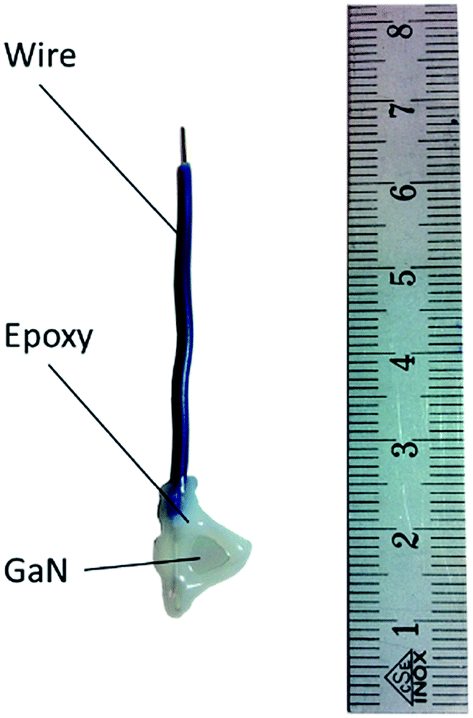 | ||
| Fig. 3 Photo of the GaN electrode. | ||
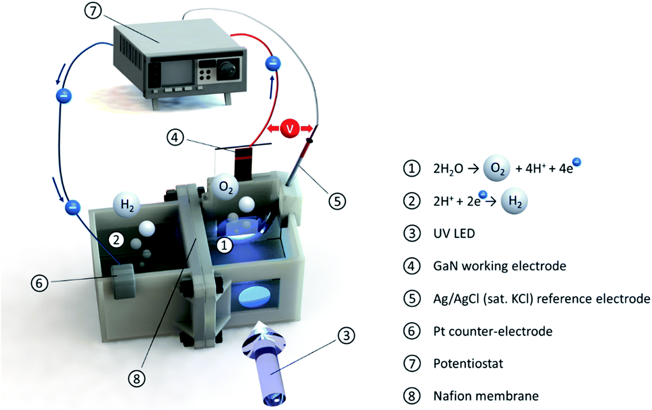 | ||
| Fig. 4 Scheme of the experimental PEC water-splitting test cell connected to the potentiostat. The UV LED illuminates the working electrode through air, quartz glass, and electrolyte. | ||
The spectral irradiance is shown in Fig. S1.† The total measured irradiance was 9.9 mW cm−2 at a distance of 4 cm from the LED of which 2.45 mW cm−2 could actually be absorbed by GaN with a bandgap of 3.39 eV (equivalent to a band gap wavelength of 365.6 nm).
The current–voltage curves were obtained using linear sweep voltammetry with a varying voltage rate of 10 mV s−1 (typically in a voltage range of −1 to 1.5 V vs. RHE). The voltage rate of 10 mV s−1 gave a stable steady-state current without any hysteresis on the photocurrent. Impedance spectra were measured at varying potentials which were scanned from −0.6 to 1 V vs. RHE covering a frequency range of 300 mHz to 1 MHz. The first run of the measurements are used (which ensured stable current conditions, see Fig. S2†) since GaN dissolves in the electrolyte after a few minutes under small current densities, i.e. around 0.5 mA cm−2.
3.4. Experimental parameter value estimation
The flatband potential and doping concentration were experimentally estimated by electrochemical impedance spectroscopy (EIS) using Mott–Schottky theory:28,31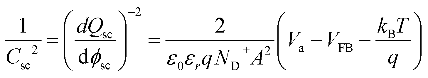 | (37) |
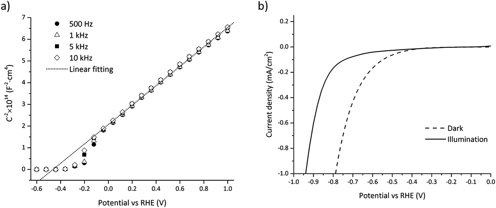 | ||
| Fig. 5 (a) Mott–Schottky plot for four frequencies (500 Hz, 1 kHz, 5 kHz, 10 kHz) of a 1 μm thick nid-GaN sample immersed in 1 M H2SO4 electrolyte under dark. (b) Experimental dark current density (dashed line) and photocurrent density (solid line) vs. RHE. | ||
The small trough around −0.5 V to −0.1 V vs. RHE depicted in Fig. 5a is assumed to result from interface states near the conduction band, i.e. the measured capacitance being the sum of the SC and the interface states capacitance.54 Interface states usually follow a Gaussian distribution which is in accordance with the observed trough (see Fig. 5a).
Interface states charging under illumination can cause a change in the flatband potential as previously mentioned and this effect has been observed for GaN in previous work.55 The shift in the flatband potential was measured by comparing the current for water reduction under dark and illumination depicted in Fig. 5b. The flatband potential shift was −0.17 V, which gave a flatband potential of −0.66 V vs. RHE under illumination.
3.5. Numerical model validation
Linear sweep voltammetry measurements and numerical simulations on GaN were used for the comparison between the steady-state numerical model and the experimental results. The surface charge transfer kinetic velocities for holes and electrons (see eqn (20) and (21)), electron and hole surface recombination lifetimes (see eqn (14)), and HER exchange current density (see eqn (32)) were estimated from linear sweep voltammetry by parameter fitting and are summarized in Table 2. The surface charge transfer velocities are smaller compared to typical semiconductor–metal interface velocities (usually in the range of 1–104 m s−1)24 as the catalytically-driven electrochemical reaction slows down the charge transfer. The small surface recombination lifetimes indicated that surface recombination is a major loss in the case of nid-GaN. The exchange current density is three orders of magnitude below state-of-art HER catalysts.22 The modeled case using parameter values indicated in Tables 1 and 2 is considered as our reference case.| Fitting parameters | Electron surface transfer kinetic velocity, vs,n | 1 × 10⁻³ m s−1 |
| Hole surface transfer kinetic velocity, vs,p | 5 × 10⁻² m s−1 | |
| Electron surface recombination lifetime, τs,n | 8 × 10⁻¹³ s | |
| Hole surface recombination lifetime, τs,p | 8 × 10⁻¹³ s | |
HER exchange current density,  |
1 × 10⁻³ mA cm−2 |
The only parameter that is changed in the experiment is the applied potential. Therefore, we compared the numerical current–potential dependency under dark and illumination with the experimental current–potential measurements. The measurements of n-GaN were stable over eight minutes during linear sweep voltammetry and at photocurrent densities bellow one mA cm−2 (see Fig. S2†). We used the first linear sweep voltammetry measurements (from 1.5 V to −1 V vs. RHE, in about 2 minutes) for experimental-numerical comparison because GaN suffers from photocorrosion in acidic solutions although it is known to be resistant to corrosion.56,57 The numerically calculated dark current compares well to the experimentally measured current as depicted in Fig. 6. The calculated slope in the photocurrent is steeper at the onset potential than the measured one. This is explained by the losses within the highly doped GaN layer used for the charge collection, which were not accounted for in the model.
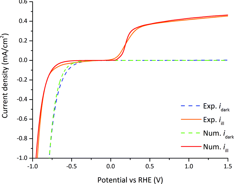 | ||
| Fig. 6 Dark current densities (dashed lines) and photocurrent densities (solid lines) vs. RHE, and comparison between experimentally measured values and numerically calculated values. | ||
Two different dark current regimes can be distinguished in Fig. 6. Above the flatband potential (−0.49 V vs. RHE) the dark current is a minority current of only a few nA since nid-GaN is naturally n-type with a negligible amount of holes to actually enable the water oxidation. Indeed, the hole dark current density is only 1.4 × 10−41 mA cm−2 (see Table 1) producing a negligible dark current. Around and below the flatband potential, the current shifts to a majority current as there is no more potential barrier with a downward bending band. In this case, the applied potential drops not only in the SC layer but also in the H layer in accordance with eqn (32).
Four different photocurrent regimes can be distinguished in Fig. 6. In the first regime at potentials between 0.4 to 1.5 V vs. RHE, the photocurrent slightly decreases from the maximum photocurrent of 0.42 mA cm−2 at 1.5 V vs. RHE to 0.37 mA cm−2 at 0.5 V vs. RHE. In this regime the current density is a minority charge carrier current, holes are transferred from the semiconductor to the electrolyte for the water oxidation reaction. The applied potential and the band bending at the semiconductor–electrolyte interface provides an electric field large enough to allow for efficient charge separation. Recombination rates represent a 27% loss on the total photo-generation rate at 1.5 V vs. RHE and 44% loss at 0.4 V vs. RHE. This non-linear current drop is mainly associated to surface recombination since τs,n/p ≪ τbulk,n/p and consequently τeff,n/p ≈ τs,n/p (see eqn (14), and Tables 1 and 2) and is explained in detail in Section 3.7. Above 0 vs. RHE, the potential drops only in the semiconductor SCR.
In the second regime at potentials between 0.4 and 0 V vs. RHE, the photocurrent abruptly decreases to zero at around 0 V vs. RHE. The electric field created by the potential and the band bending is not sufficient for charge separation and electron–hole recombination starts to dominate. Recombination rates represent a 50% loss on the total photo-generation rate at 0.28 V vs. RHE and a 100% loss at 0.05 V vs. RHE.
In the third regime between potentials at 0 V and −0.66 V vs. RHE, the band bending starts to decrease until reaching the flatband potential conditions at −0.66 V vs. RHE. The recombination of electron and holes is complete and there is no photocurrent.
In the fourth regime between potentials −0.66 and −1.0 V vs. RHE, the current becomes a majority carrier current because of the downward band bending. Electrons are transferred from the semiconductor to the electrolyte for the water reduction reaction. The current decreases exponentially following eqn (21). The applied potential below the flatband potential drops not only in the SCR, but also in the HL layer in accordance with eqn (32). This behavior is consistent with the dark condition, only the flatband potential shifts between dark and illumination.
In addition to predicting the experimental values accessible by measurements, the benefit of the numerical model is that it allows for the prediction of the depth-dependent charge carrier generation, the depth-dependent electron and hole concentrations, and the depth-dependent energy levels of the quasi-Fermi levels, conduction band, and valence band in the semiconductor. Fig. S3–S5† show the distribution of these parameters for the reference case under illumination at 0 V vs. RHE. The current is also depicted in Fig. 6 (red curve at 0 V vs. RHE). The accessibility of such concentration and energy profiles greatly supports the understanding and interpretation of the observed current–voltage behavior.
3.6. Numerical design of experiment
The FFD was used to screen for the most influential semiconductor and semiconductor–electrolyte interface parameters on the photocurrent, i.e. fourteen parameters with two levels as presented in Table 3. The minimum and maximum values were carefully chosen to lie within realistic limits as otherwise no convergence in the numerical solution was achieved. The baseline parameters were required to lie between the upper and lower limits.| Parameters | Unit | Minimum | Maximum |
|---|---|---|---|
| Electron surface transfer kinetic velocity, νs,n | m s−1 | 1 × 10⁻⁴ | 1 × 10⁻² |
| Hole surface transfer kinetic velocity, νs,p | m s−1 | 1 × 10⁻² | 1 × 10⁻¹ |
| Direct recombination factor, Cdir | cm3 s−1 | 1 × 10⁻⁹ | 1 × 10⁻⁷ |
| Effective electron lifetime, τeff,n | s | 1 × 10⁻¹³ | 1 × 10⁻¹¹ |
| Effective hole lifetime, τeff,p | s | 1 × 10⁻¹³ | 1 × 10⁻¹¹ |
| Electron Auger recombination factor, Caug,n | cm6 s−1 | 1 × 10⁻³³ | 1 × 10⁻³¹ |
| Hole Auger recombination factor, Caug,p | cm6 s−1 | 1 × 10⁻³³ | 1 × 10⁻³¹ |
| Donor concentration, ND+ | cm−3 | 1 × 10¹⁶ | 1 × 10¹⁷ |
| Flatband potential, VFB | V vs. RHE | −0.5 | −0.7 |
| Relative permittivity, εr | — | 7 | 11 |
| Semiconductor film thickness, d | μm | 0.8 | 1.2 |
| Hole mobility, μp | cm2 V−1 s−1 | 50 | 200 |
| Effective density of states, valence band, NV | cm−3 | 8 × 10¹⁷ | 6 × 10¹⁸ |
| Effective density of states, conduction band, NC | cm−3 | 1 × 10¹⁹ | 8 × 10¹⁹ |
In order to ensure that the residuals were normally distributed, transformations in the photocurrent results were performed at both potentials investigated, i.e. 0.3 V and 1.23 vs. RHE. At 0.3 V vs. RHE, a power function, y′ = (y + k)λ, with k = 0.0057 and λ = 0.61 was used as the transformation function. At a potential of 1.23 V vs. RHE, a power function with k = 0 and λ = 1.99 was used. At both potentials, the normal plot of the residuals indicated no abnormalities and the R2 coefficients for a normal distribution were reasonable (0.95 for 1.23 V vs. RHE and 0.88 for 0.3 V vs. RHE). The residuals versus predicted values plots showed an approximately constant level of the studentized residuals across all predicted values and no outliers were found outside of the 95% confidence control limit in the studentized residuals versus run plot. Hence, the multiple regression model could be validated and the influence of each parameter could be safely investigated.
The Pareto charts depicted in Fig. 7 show the significant parameters or interactions, i.e. parameters or interactions with an effect above the Bonferroni limit. The most relevant factors at 1.23 V vs. RHE are, from the largest to the smallest influence: τeff,p, τeff,n, the interaction between effective hole and doping concentration τeff,n·ND+, and ND+ (Fig. 7a). The other significant effects like the interaction between effective electron and hole lifetime, τeff,n·τeff,p, and μp are also presented in Fig. 7a although their effects are lower compared to the effective lifetimes and the doping concentration. The bulk lifetimes are measured values45 which are intrinsic properties of GaN, but the lifetimes related to the surface recombination process depend on the semiconductor–electrolyte interface. The surface recombination lifetimes were more than three orders of magnitude lower than the bulk recombination and dominated the effective lifetimes (see Tables 1 and 2). Increasing the surface recombination lifetimes has a positive effect on the photocurrent (white bar in Fig. 7a) and can practically be obtained by surface passivation or by application of catalyst. The negative effect on photocurrent of the combined effective electron and hole lifetime (τeff,n·τeff,p) is explained by the non-linear dependence of these parameters on the photocurrent, inconsistent with the FFD assumption of linearity.
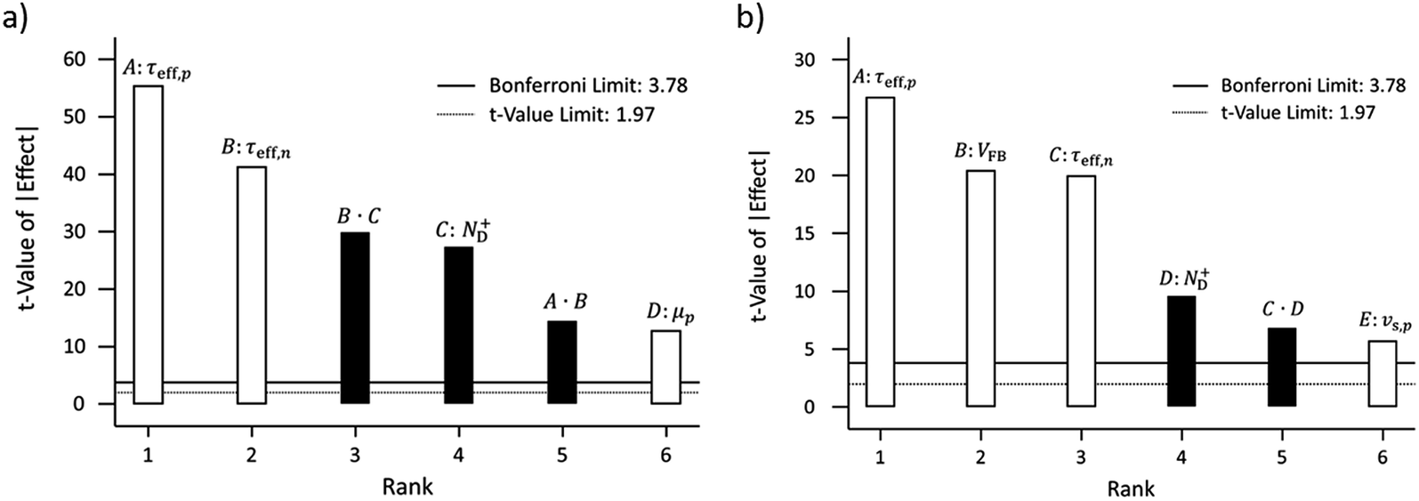 | ||
| Fig. 7 Pareto plots indicating the significance of the photocurrent response at a potential of 1.23 V (a) and 0.3 V (b) vs. RHE calculated utilizing the FFD of experiment. White bars indicate an increase and black bars a decrease, respectively, of the photocurrent when increasing the corresponding parameter. τeff,n and τeff,p are effective electron and hole lifetimes, ND+ is the doping concentration, and μp is the hole mobility, VFB, is the flatband potential, and νs,p is the hole surface transfer kinetic velocity. | ||
For the combined effect of effective electron lifetime and doping concentration (τeff,n·ND+), the negative effect of the doping concentration on the photocurrent is dominant. A more clear dependence of the most significant parameters on the photocurrent is investigated in the parametric study in the next section.
We used an effective lifetime combining surface recombination and SRH bulk recombination (see eqn (14)) and therefore the charge carrier concentration in the semiconductor is related to the surface lifetimes. Consequently, the observed strong dependence on doping concentration is a result of the effective lifetime assumption and not necessarily a physical result.
The most significant parameters influencing the photocurrent at 0.3 V vs. RHE are, from the largest to the smallest influence: τeff,p, VFB, and τeff,n (Fig. 7b). The other significant effects are also indicated: ND+, the interaction between effective electron lifetime and doping concentration τeff,n·ND+, and vs,p. According to FFD, it is beneficial for the photocurrent at 0.3 V vs. RHE to reduce the effective recombination of electrons and holes (dominated by surface lifetimes), and to increase the flatband potential.
3.7. Parametric analysis on key factors
A parametric study was done to precisely understand the functional dependence of the photocurrent on the most significant parameters according to FFD, i.e. the surface lifetimes of electrons and holes and the doping concentration at 1.23 V vs. RHE, and the surface lifetimes of the electrons and holes and the flatband potential at 0.3 V vs. RHE.The influence of the hole surface lifetime on the photocurrent for varying applied potential is presented in Fig. 8. An increase of the hole surface lifetime has not only the beneficial effect of shifting the onset potential but also allows the further increase of the photocurrent at larger applied potentials. This unusual effect for an OER photocatalyst has been observed for hematite and TiO2 photoelectrodes whose surfaces were modified with phosphate ions.58,59 In both cases surface phosphate ions appeared to prolong the lifetime of holes on the surface. Interestingly, our numerical model is consistent with this effect using GaN as a reference model system for small hole surface lifetimes (around 1 ps). At larger hole surface lifetimes (above 0.1 to 1 ns), the current–potential dependency follows the expected behavior, namely that surface recombination is negligible for an applied potential above 0.2 V vs. RHE.
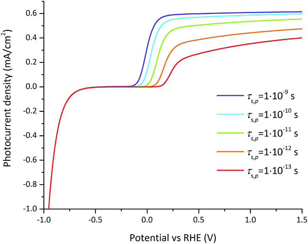 | ||
| Fig. 8 Photocurrent–voltage curves for varying hole surface lifetimes for the reference case (parameters indicated in Tables 1 and 2). For large hole surface lifetimes (above 0.1 to 1 ns), surface recombination is negligible at large applied potentials. For small hole surface lifetimes (around 1 ps), the photocurrent is still affected by surface recombination at large potentials. | ||
The dependence of the photocurrent densities at 1.23 V vs. RHE on surface lifetimes and doping concentration are depicted in Fig. 9. At low doping concentration, i.e. 1 × 1016 cm−3 for GaN, an increase of the effective hole and electron surface lifetimes results in an increase in photocurrent (Fig. 9). If the electron surface lifetime is large enough, e.g. 1 ns, the hole surface lifetime has a less significant impact on the photocurrent; a relative increase by 9.5% (0.06 mA cm−2) for 4 orders of magnitude difference of hole surface lifetime is observed (violet line in Fig. 9). For low electron surface lifetime, e.g. 0.1 ps, increasing the hole surface lifetime from 1 ps to 0.1 ns increases the photocurrent by 0.34 mA cm−2, which represents a relative increase of 58%. Increasing the doping concentration to 1 × 1018 cm−3 results in a photocurrent which is not affected by the electron surface lifetime (Fig. 9). On the other hand, the hole surface lifetime is still significant at these larger doping concentrations, i.e. increasing the hole surface lifetime from 1 ps to 1 ns increases the photocurrent by 0.21 mA cm−2.
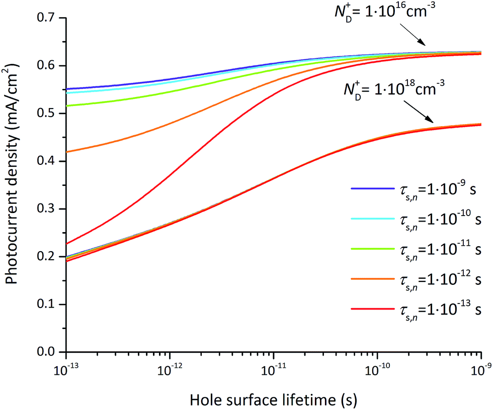 | ||
| Fig. 9 Photocurrent density at 1.23 V vs. RHE as a function of the hole surface lifetime for various electron lifetimes (τs,n = 10−9, 10−10, 10−11, 10−12, 10−13 s) and two doping concentrations (ND+ = 1016 cm−3 and ND+ = 1018 cm−3). | ||
The photocurrent, being a minority current, is generally more influenced by the hole surface lifetime. Especially at large hole surface lifetimes, the influence of electron surface lifetime becomes negligible. The insensitivity of the photocurrent on electron surface lifetime at high doping concentrations results from the dominating terms in the recombination, namely the electron concentration and hole surface lifetime (see eqn (11)). As mentioned, the photocurrent results from the combined influence of the numerical value of the hole surface lifetime, electron surface lifetime, and doping concentration. Therefore under low doping and low hole surface lifetime the electron surface lifetime can still have an impact on the photocurrent at 1.23 V which appears counterintuitive.
The doping concentration-dependent current–voltage behavior under illumination is depicted in Fig. 10. An optimal doping concentration is found at a value of ND+ = 1016 cm−3 above about 0.2 V vs. RHE as depicted in Fig. S6.† The optimum is caused by different and opposing effects. On one hand a decrease of the doping concentration leads to a lower Fermi level. Since the Fermi level aligns with the interface states located at the semiconductor–electrolyte interface, it leads to a higher band bending at the semiconductor–electrolyte interface and therefore a positive shift of the onset potential and an increase of the photocurrent (can be clearly observed on the negative potential side). On the other hand, the recombination rate increases with larger doping concentrations simply because of the increased electron concentration which reduces the photocurrent. At very low doping concentrations, the semiconductor is completely depleted and there is no band bending but instead a linearly increasing band potential throughout the entire semiconductor. By assuming locally a constant potential change and by integrating the drift-diffusion equations (eqn (7) and (8)) within the semiconductor, the current–potential relation is predicted by Ohm's law. This situation is depicted in Fig. 10 at a doping concentration of ND+ = 1014 cm−3 where the photocurrent versus potential starts to show a linear trend. These effects must be considered when optimizing the photocurrent density by variations in doping concentration and operating potential. For example at an operating potential of 0.3 V vs. RHE, the photocurrent density increases by 0.25 mA cm−2 by changing the doping concentration from 1014 cm−3 to 1016 cm−3 which represents a relative gain of 69%.
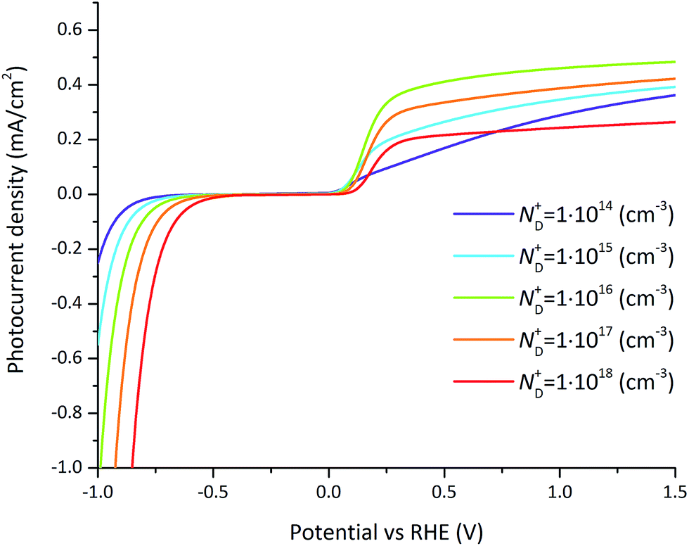 | ||
| Fig. 10 Photocurrent–voltage curves for varying doping concentration for the reference case (parameters indicated in Tables 1 and 2). For small doping concentrations (bellow 1014 cm−3), the photocurrent–potential relation is linear. For intermediate doping concentrations (around 1016 cm−3), the photocurrent shows an optimum at which the band bending is maximized and recombination is reasonable. At large doping concentrations (above 1018 cm−3) recombination dominates. | ||
The photocurrent densities at 0.3 V vs. RHE depend most significantly on the flatband potential, electron lifetime, and hole surface lifetime. The variation of the flatband potential gives rise to a shift of the onset potential (see Fig. S7†). A more complex behavior is observed when also varying the surface lifetimes as depicted in Fig. 11. At a flatband potential of −0.5 V, the band bending is reduced resulting in a decreased electric field and consequently a decreased hole transfer from the semiconductor to the electrolyte (the photocurrent). Since the electric field is lower, recombination becomes the dominating loss which is directly related to the hole and electron surface lifetimes (Fig. 11a).
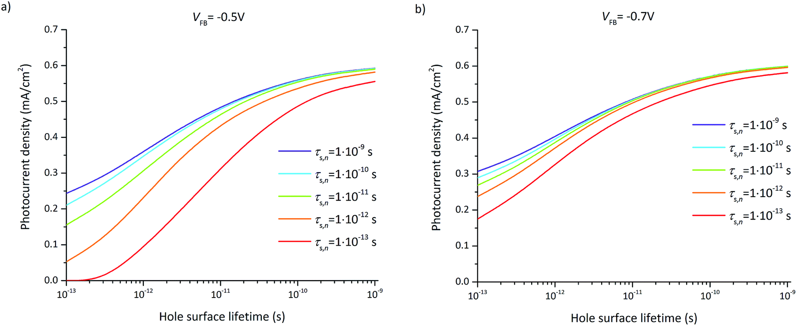 | ||
| Fig. 11 Photocurrent density at 0.3 V vs. RHE as a function of the hole surface lifetime for various electron lifetimes (τs,n = 10−9, 10−10, 10−11, 10−12, 10−13 s) and two flatband potentials: (a) VFB = −0.5 V vs. RHE, and (b) VFB = −0.7 V vs. RHE. | ||
A significant effect of the hole surface lifetime on the photocurrent is observed at a flatband potential of −0.5 V vs. RHE (Fig. 11a). At low electron lifetime, i.e. 0.1 ps, the photocurrent increases from 0 mA cm−2 to 0.56 mA cm−2 when changing the hole surface lifetime by four orders of magnitude, i.e. from 0.1 ps to 1 ns. Even at higher electron surface lifetime, i.e. 1 ns, the photocurrent increases from 0.24 mA cm−2 to 0.54 mA cm−2 (a relative increase of 55%) when increasing the hole surface lifetime from 0.1 ps to 1 ns. The behavior is similar at a flatband potential of −0.7 V vs. RHE (Fig. 11b), although the electron and hole surface lifetimes have a smaller impact: the photocurrent increases by 0.4 mA cm−2 (from 0.18 mA cm−2 to 0.58 mA cm−2, i.e. a relative increase of 69%) when increasing the hole surface lifetime from 0.1 ps to 1 ns at an electron surface lifetime of 0.1 ps. At an electron surface lifetime of 1 ns, the photocurrent increases by 0.29 mA cm−2 (a relative increase of 48%) when increasing the hole surface lifetime from 0.1 ps to 1 ns.
4. Summary and conclusion
A multi-physics model of a semiconductor water-splitting photoelectrode immersed in electrolyte was developed. The model coupled electromagnetic wave propagation, charge carrier generation and transport, and charge transfer at the semiconductor–electrolyte interface. The model provided, among others, spatially resolved energy band diagrams, charge carrier concentrations, and generation and recombination profiles in the semiconductor. The model incorporated an adapted Schottky contact at the semiconductor–electrolyte interface, accounting for pinning and unpinning of the band edges and for potential drop within the SCR as well as the HL. The interface model presented allows for a straightforward extension to semiconductor–catalyst–solution systems with metallic, adaptive and molecular catalysts by using the boundary conditions presented in the work of Mills et al.13 The HL played only a role in charge transfer at the semiconductor–electrolyte interface for majority carrier currents. In this case, the potential distribution between the HL and the SCR was determined by a newly derived analytical solution.The numerical model was applied to our model system composed of a non-intentionally doped n-type gallium nitride (GaN) with wurtzite crystal structure photoelectrode layer immersed in 1 M sulfuric acid. GaN was chosen here as it allows for unbiased photoelectrochemical water-splitting. Additionally, GaN has been shown to be considerably resistant to corrosion in many solutions in the dark49 although it gradually dissolves under illumination. GaN has been known to have interface states, therefore flatband potentials under dark and illumination were experimentally determined by electrochemical impedance spectroscopy using Mott–Schottky theory. Flatband potentials under dark and illumination were found to be −0.49 V and −0.66 V vs. RHE. Impedance spectroscopy was also used to estimate the intrinsic doping concentration of nid-GaN, estimated as 4 × 1016 cm−3. Linear sweep voltammetry was then used to determine photocurrent response as a function of the applied potential to which the modeled photocurrent–potential response was compared in order to validate the multi-physics model.
The multi-physics model allowed representation of numerous semiconductor materials with numerous semiconductor–electrolyte interface properties such as electron and hole mobilities, surface lifetimes, flatband potential, permittivity, doping concentration, bulk SRH recombination, and hole and electron interface kinetics. The large number of relevant material and interface characteristics renders the identification of the most significant parameter(s) challenging. Statistical tools provide a pathway for solving this challenge as demonstrated in this study. The validated model was used in a FFD of experiment to statistically identify the most significant material and interface parameters and device dimensions on the photocurrent. Key factors were identified at two different potentials: 0.3 V vs. RHE and 1.23 V vs. RHE. Hole and electron surface lifetimes and doping concentration appeared to be the most significant factors at 1.23 V vs. RHE. At 0.3 V vs. RHE, hole and electron surface lifetimes and flatband potential were the most significant factors. The statistically identified most significant parameters were further investigated and theoretically optimized in a detailed parameter study. The parametric analysis provided quantifiable effects and functional dependence of the photocurrent on the predominant factors previously determined by FFD analysis.
The developed methodology uses an experimentally-validated numerical model and statistical analysis to provide understanding of the performance of water-splitting photoelectrodes. It allows for the identification of the most significant parameters on performance. Subsequent in-depth parametric analysis of the most significant parameters allows for the quantification of their effect and subsequent optimization of the device for maximum performance. The presented methodology provides a general approach to identify and quantify main material challenges and design considerations in functioning water-splitting photoelectrodes. The predictive character of the validated model can be further exploited with confidence to approach and investigate morphologically complex electrodes and material classes for which research-related questions are not yet answered.
Conflict of interest
The authors declare no competing financial interest.Acknowledgements
The authors would like to acknowledge the funding from the National Science Foundation under Grant #200021_159547. The authors would like to thank Dr Thomas Moehl (LPI at EPFL), for helpful discussions on electrochemical impedance spectroscopy, Dr Jean-François Carlin (LASPE at EPFL) for the deposition of nid-GaN on sapphire substrate, and Dr Mikaël Dumortier (LRESE at EPFL) and Dr Simone Pokrant (EMPA) for fruitful discussions.References
- K. Sivula, Chimia, 2013, 67, 155–161 CrossRef CAS PubMed.
- M. A. Modestino and S. Haussener, Annu. Rev. Chem. Biomol. Eng., 2014, 6, 13–34 CrossRef PubMed.
- T. J. Jacobsson, V. Fjällström, M. Edoff and T. Edvinsson, Energy Environ. Sci., 2014, 7, 2056–2070 CAS.
- M. G. Walter, E. L. Warren, J. R. McKone, S. W. Boettcher, Q. Mi, E. a. Santori and N. S. Lewis, Chem. Rev., 2010, 110, 6446–6473 CrossRef CAS PubMed.
- A. C. Nielander, M. R. Shaner, K. M. Papadantonakis, S. a. Francis and N. S. Lewis, Energy Environ. Sci., 2015, 8, 16–25 CAS.
- A. J. Nozik and R. Memming, J. Phys. Chem., 1996, 100, 13061–13078 CrossRef CAS.
- J.-N. Chazalviel, J. Electrochem. Soc., 1982, 129, 963–969 CrossRef CAS.
- D. Vanmaekelbergh, Electrochim. Acta, 1997, 42, 1121–1134 CrossRef CAS.
- D. Vanmaekelbergh, Electrochim. Acta, 1997, 42, 1135–1141 CrossRef CAS.
- M. N. Latto, G. Pastor-Moreno and D. J. Riley, Electroanalysis, 2004, 16, 434–441 CrossRef CAS.
- J. Reichman, Appl. Phys. Lett., 1980, 36, 574–577 CrossRef CAS.
- R. Memming, Semiconductor Electrochemistry, Wiley-VCH, Weinheim, 2001 Search PubMed.
- T. J. Mills, F. Lin and S. W. Boettcher, Phys. Rev. Lett., 2014, 112, 148304 CrossRef PubMed.
- P. Cendula, S. D. Tilley, S. Gimenez, J. Bisquert, M. Schmid, M. Grätzel and J. O. Schumacher, J. Phys. Chem. C, 2014, 118, 29599–29607 CAS.
- A. Berger and J. Newman, J. Electrochem. Soc., 2014, 161, 3328–3340 CrossRef.
- F. E. Osterloh, Chem. Soc. Rev., 2013, 42, 2294–2320 RSC.
- T. Lopes, L. Andrade, F. Le Formal, M. Gratzel, K. Sivula and A. Mendes, Phys. Chem. Chem. Phys., 2014, 16, 16515–16523 RSC.
- R. Siegel and J. Howell, Thermal radiation heat transfer, Taylor & Francis, London, 4th edn, 2001 Search PubMed.
- J. Newman and K. E. Thomas-Alyea, Electrochemical Systems, John Wiley & Sons, Inc., 3rd edn, 2001 Search PubMed.
- A. J. Bard and L. R. Faulkner, Electrochemical Methods: Fundamentals and Application, John Wiley & Sons, Inc., 2nd edn, 2001 Search PubMed.
- K. J. Vetter, Electrochemical Kinetics Theoretical and Experimental Aspects, Academic Press Inc., 1967 Search PubMed.
- S. Haussener, C. Xiang, J. M. Spurgeon, S. Ardo, N. S. Lewis and A. Z. Weber, Energy Environ. Sci., 2012, 5, 9922–9935 CAS.
- D. M. Pozar, Microwave Engineering, 4th edn, 2012 Search PubMed.
- K. K. N. S. M. Sze, Physics of semiconductor devices, Wiley-inte, 2007 Search PubMed.
- K. Gullbinas, V. Grivickas, H. P. Mahabadi, M. Usman and A. Hallen, Mater. Sci., 2011, 17, 119–124 CrossRef.
- A. B. Sproul, J. Appl. Phys., 1994, 76, 2851–2854 CrossRef CAS.
- D. J. Michalak, F. Gstrein and N. S. Lewis, J. Phys. Chem. C, 2008, 112, 5911–5921 CAS.
- R. van de Krol and M. Grätzel, Photoelectrochemical Hydrogen Production, Springer, New York, 2012 Search PubMed.
- R. Memming, Semiconductor Electrolyte, Wiley-VCH, 1999 Search PubMed.
- A. Hagfeldt, U. Björkstén and M. Grätzel, J. Phys. Chem., 1996, 100, 8045–8048 CrossRef CAS.
- K. Gelderman, L. Lee and S. W. Donne, J. Chem. Educ., 2007, 84, 685–688 CrossRef CAS.
- L. Ivanova, S. Borisova, H. Eisele, M. Dähne, a. Laubsch and P. Ebert, Appl. Phys. Lett., 2008, 93, 7–10 CrossRef.
- C. G. Van De Walle and D. Segev, J. Appl. Phys., 2007, 101, 081704 CrossRef.
- Comsol Multiphysics v5.0, 2015.
- D. C. Montgomery, Design and Analysis of Experiments, John Wiley & Sons, Inc., New York, 7th edn, 2008 Search PubMed.
- State-Ease Design Expert v9, 2015.
- A. Nicolet, S. Guenneau, C. Geuzaine and F. Zolla, J. Comput. Appl. Math., 2004, 168, 321–329 CrossRef.
- E. A. B. Cole, Mathematical and Numerical Modelling of Heterostructure Semiconductor Devices: From Theory to Programming, Springer, 2009 Search PubMed.
- S. Adachi, Optical Constants of Crystalline and Amorphous Semiconductors: Numerical Data and Graphical Information, Kluwer Academic Publishers, Norwell, MA, 1999 Search PubMed.
- G. M. Hale and M. R. Querry, Appl. Opt., 1973, 12, 555–563 CrossRef PubMed.
- S. Nakamura and M. R. Krames, Proc. IEEE, 2013, 101, 2211–2220 CrossRef CAS.
- J. I. Pankove, S. Bloom and G. Harbeke, RCA Rev., 1975, 36, 163 CAS.
- S. Bloom, G. Harbeke, E. Meier and I. B. Ortenburger, Phys. Status Solidi, 1974, 66, 161–168 CrossRef CAS.
- J. F. Muth, J. H. Lee, I. K. Shmagin, R. M. Kolbas, H. C. Casey, B. P. Keller, U. K. Mishra and S. P. DenBaars, Appl. Phys. Lett., 1997, 71, 2572–2574 CrossRef CAS.
- J. Piprek, R. Sink, M. A. Hansen, J. E. Bowers and S. P. DenBaars, Proc. SPIE, 2000, 3944, 3912–3944 CrossRef.
- P. Mackowiak and W. Nakwaski, MRS Internet J. Nitride Semicond. Res., 1998, 3, 1–10 Search PubMed.
- V. Bougrov, M. E. Levinshtein, S. L. Rumyantsev and A. Zubrilov, Properties of Advanced Semiconductor Materials GaN, AlN, InN, BN, SiC, SiGe, John Wiley & Sons, New York, 2001, vol. 1 Search PubMed.
- T. P. Chow and M. Ghezzo, SiC Power Devices in III-Nitride, SiC and Diamond Materials for Electronic Devices, Material Research Society Symposium Proceedings, Pittsburg, PA, 1996, vol. 423 Search PubMed.
- M. Ono, K. Fujii, T. Ito, Y. Iwaki, A. Hirako, T. Yao and K. Ohkawa, J. Chem. Phys., 2007, 126, 054708 CrossRef PubMed.
- M. Rubin, N. Newman, J. S. Chan, T. C. Fu and J. T. Ross, Appl. Phys. Lett., 1994, 64(1), 64–66 CrossRef CAS.
- M. Ono, K. Fujii, T. Ito, Y. Iwaki, A. Hirako, T. Yao and K. Ohkawa, J. Chem. Phys., 2007, 126, 054708 CrossRef PubMed.
- A. Nakamura, M. Sugiyama, K. Fujii and Y. Nakano, Jpn. J. Appl. Phys., 2013, 52, 08JN20 CrossRef.
- O. Madelung, U. Rössler, D. Strauch and S. Adachi, Group IV elements, IV–IV and III–V compounds, Springer, 2001 Search PubMed.
- P. Stallinga, Electrical Characterization of Organic Electronic Materials and Devices, John Wiley & Sons, Chichester, 2009 Search PubMed.
- J. J. Kelly and R. Memming, J. Electrochem. Soc., 1982, 129, 730–738 CrossRef CAS.
- Light, Water, Hydrogen, ed. C. A. Grimes, O. K. Varghese and S. Ranjan, Springer, New York, 2008 Search PubMed.
- S. S. Kocha, M. W. Peterson, D. J. Arent, J. M. Redwing, M. A. Tischler and J. A. Turner, J. Electrochem. Soc., 1995, 142, 238–240 CrossRef.
- J. Y. Kim, J.-W. Jang, D. H. Youn, G. Magesh and J. S. Lee, Adv. Energy Mater., 2014, 4, 1–7 Search PubMed.
- L. Jing, J. Zhou, J. R. Durrant, J. Tang, D. Liu and H. Fu, Energy Environ. Sci., 2012, 5, 6552–6558 CAS.
Footnote |
| † Electronic supplementary information (ESI) available. See DOI: 10.1039/c5ta07328f |
| This journal is © The Royal Society of Chemistry 2016 |