
 Open Access Article
 This Open Access Article is licensed under a Creative Commons Attribution-Non Commercial 3.0 Unported Licence
The impact of grafted surface defects and their controlled removal on supramolecular self-assembly†
Ana M.
Bragança
 a,
John
Greenwood
*a,
Oleksandr
Ivasenko
*a,
Thanh Hai
Phan
ab,
Klaus
Müllen
c and
Steven
De Feyter
*a
a,
John
Greenwood
*a,
Oleksandr
Ivasenko
*a,
Thanh Hai
Phan
ab,
Klaus
Müllen
c and
Steven
De Feyter
*a
aDepartment of Chemistry, Division of Molecular Imaging and Photonics, KU Leuven-University of Leuven, Celestijnenlaan 200F, B-3001 Leuven, Belgium. E-mail: john.greenwood@kuleuven.be; oleksandr.ivasenko@kuleuven.be; steven.defeyter@kuleuven.be
bDepartment of Physics, Quynhon University, 170 An Duong Vuong, Quynhon, Vietnam
cMax Planck Institute for Polymer Research, 55128 Mainz, Germany
First published on 25th July 2016
Abstract
We demonstrate the use of covalently modified graphite as a convenient and powerful test-bed for the versatile investigation and control of 2-D crystallization at the liquid solid interface. Grafted aryls act as surface defects and create barriers to supramolecular self-assembly. An easily tunable grafting density allows for varying the effect of such defects on supramolecular self-assembly. Finally, the defects can be locally removed, triggering monolayer reconstructions and allowing in situ investigations of thermodynamically unstable or metastable morphologies.
Introduction
Supramolecular self-assembly is an intensively studied topic and can be applied towards 2-D crystal engineering on atomically flat solid surfaces,1–4 enabling the formation of multiple architectures with potential nanotechnology applications.5–8 Control over the quality of molecular networks is a crucial necessity to tune surface or interfacial properties. This includes the formation of large defect-free crystals in organic semiconductors, which are important for high performance organic thin-film transistors.9Common methods to control the quality of crystalline thin films on pristine and ideal surfaces include careful design of the building blocks10 as well as finding optimal self-assembly conditions by varying the temperature,11,12 solute concentration,13 type of solvent,14,15 solvent flow,16 and substrate.17 All of these parameters directly influence the nucleation, growth and/or ripening stages of 2-D crystallization. However, surface defects might affect these processes.
Surface defects are often inherent to surface systems. They can be the result of non-ideal production processes, including contamination, or they are intrinsic to a material, and it may be impossible to avoid or remove them. These defects are often detrimental to the 2-D monolayer crystal quality and associated advantageous properties. They affect the quality of the self-assembled monolayers by creating structural barriers to the formation of large domains. For example, the polycrystalline nature of a substrate is shown to induce grain boundaries and dislocations within a self-assembled monolayer.18
To gain insight into the role of defects and the way they affect 2-D crystallization, and to find ways to minimize their impact, it is important to come up with a test system that allows control of the surface defect density and to remove defects in a controlled fashion.
In this study, by following a unique approach, we control the surface density of defects on graphite, and investigate the impact on monolayer nucleation and growth of a model molecular system. The defects are created by covalently grafting aryl radicals on a substrate, and their impact on 2-D crystal formation is probed using 5-octadecyloxy-isophthalic acid (ISA-OC18). The study reveals the importance of defect density and the various ways it impacts monolayer nucleation, growth, and ripening. We uncover the role of annealing in relation to defect densities. In addition, in situ removal of individual grafted species enables the control of 2-D crystallization processes with nanoscale precision. Our approach, using scanning tunneling microscopy (STM) as an imaging and nanolithography tool, provides novel opportunities to study and control self-assembly phenomena on surfaces.
Results and discussion
Recently, we have demonstrated that 3,5-di-tert-butylphenyl radicals (generated via electrochemical reduction of the corresponding aryldiazonium salt, 3,5-TBD, Fig. 1A and C) can covalently graft onto graphene and highly oriented pyrolytic graphite (HOPG).19 Visualized with STM and atomic force microscopy (AFM), the grafted aryls appear as bright blobs (herein referred to as pins) 0.7 nm and 1–2 nm in height and width, respectively. The exact number of aryls within each pin is not known (most likely one or two).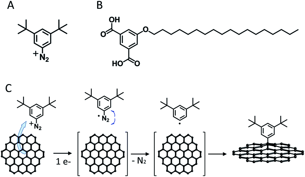 | ||
| Fig. 1 Molecular structure of: (A) 3,5-bis-tert-butylbenzenediazonium (3,5-TBD), and (B) 5-octadecyloxy-isophthalic acid (ISA-OC18). (C) Reaction scheme for the generation and covalent attachment of 3,5-di-tert-butylphenyl radicals to the carbon surface. | ||
Grafting appears to be random (see Section S2 in the ESI†), and the surface density of the pins can be easily varied for a wide range of values. Grafted species have high stability and are not affected by the self-assembly of supramolecular building blocks at the liquid–solid interface. Furthermore, we demonstrated that using very mild STM lithography, the pins can be locally removed with nanoscale resolution. These properties inspired us to test the applicability of such grafted surfaces in the investigation of 2-D crystallization at the liquid–solid interface.
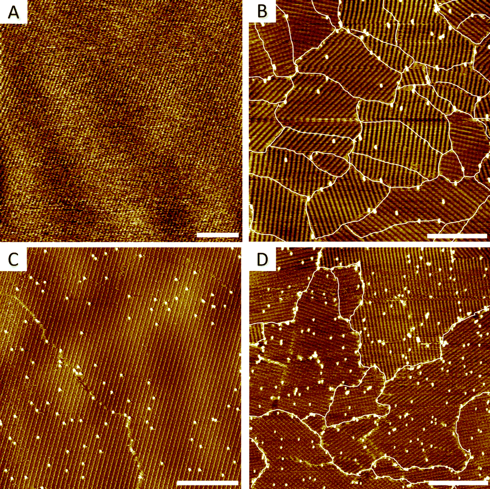
As a model system for this study we chose 5-octadecyloxy-isophthalic acid (ISA-OC18, Fig. 1B). Its self-assembly on HOPG has been thoroughly investigated before,20–23 allowing the convenient selection of optimal conditions for self-assembly. The concentration of ISA-OC18 in octanoic acid solution was set to 0.2 mM. At room temperature (20 °C) on bare HOPG, the self-assembly yields ∼1500–4000 nm2 sized domains, easily distinguishable on large scale STM images (200 nm × 200 nm), shown in Fig. 2A. All domains belong to the same polymorph, consisting of H-bonded double-rows of isophthalic acid moieties and lamellar interdigitation of the alkoxy chains (Fig. 2B). Based on the surface density (ρN) of the pins, all of the grafted samples were arbitrarily split into two groups: (1) samples with a low surface density of pins (ρN = 1500–6000 pins per μm2, Fig. 2C), and (2) samples with a high surface density of pins (ρN = 13![[thin space (1/6-em)]](https://www.rsc.org/images/entities/char_2009.gif) 000–22000 pins per μm2, Fig. 2D).
000–22000 pins per μm2, Fig. 2D).
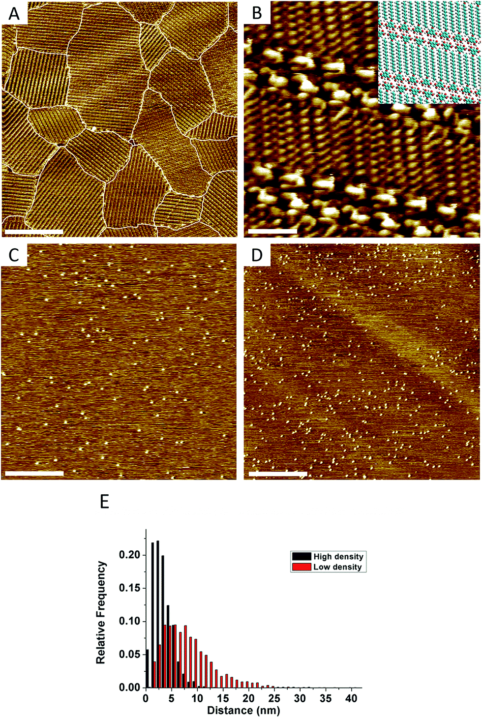 | ||
| Fig. 2 STM images of: (A) ISA-OC18 (0.2 mM) self-assembly, at 20 °C, on bare HOPG (Vs = −0.700 V, It = 80 pA, and scale bar = 50 nm) and (B) close up view together with molecular model (inset) of ISA-OC18 self-assembly (Vs = −0.675 V, It = 100 pA, and scale bar = 1.5 nm). HOPG samples with (C) low-density (Vs = −0.700 V, It = 80 pA, and scale bar = 50 nm) and (D) high-density grafting (Vs = −0.700 V, It = 70 pA, and scale bar = 50 nm). (E) Histogram revealing the distributions of the nearest-neighbour distances of the pins on HOPG with low- and high-density grafting. | ||
Upon adsorption, ISA-OC18 molecules assemble on grafted surfaces covering the areas between the pins. Since grafting is random, different combinations of pin/ISA-OC18 orientations are observed. In some cases the pins are located inside of the domains displacing few (2 to 6) ISA-OC18 molecules and disrupting normal H-bonding (Fig. 3A) and/or alkyl chain interdigitation (Fig. 3B) of the related lamellae. Occasionally, the pins promote the formation of stacking faults (Fig. 3C) that propagate over several lamellae within the domain. Grouped together, several pins can create large holes in the 2-D crystals (Fig. 3D). Finally, many pins are localized at the inter-domain borders (Fig. 3E).
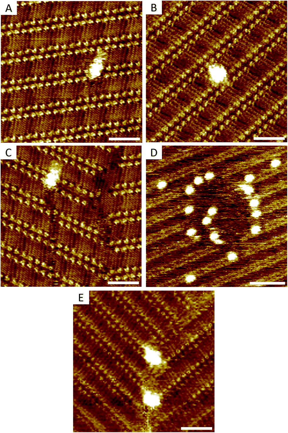 | ||
| Fig. 3 STM images of different combinations of pin/ISA-OC18 interactions: pins inside the domains disrupting (A) H-bonding (Vs = −0.700 V, It = 80 pA, and scale bar = 4 nm) or (B) alkyl chain interdigitation (Vs = −0.700 V, It = 79 pA, and scale bar = 4 nm); pins causing (C) stacking faults (Vs = −0.700 V, It = 80 pA, and scale bar = 4 nm) or (D) holes within the domain (Vs = −0.675 V, It = 80 pA, and scale bar = 8 nm); pins located at (E) the inter-domain borders (Vs = −0.710 V, It = 80 pA, and scale bar = 4 nm). | ||
The ability of a 2-D crystal to grow around defect sites decreases when the number of randomly distributed defects increases. To demonstrate this, we compared the ISA-OC18 assemblies on the samples with a low (ρN = 1500–6000 pins per μm2, Fig. 4A) and high (ρN = 13000–22000 pins per μm2, Fig. 4B) surface density of the defects. The histogram in Fig. 4C shows that the difference is quite dramatic: while low grafting does not markedly affect the size distribution of the ISA-OC18 domains compared to the ISA-OC18 self-assembly at 20 °C on bare HOPG (occasionally reaching 10000 nm2), the highly grafted samples contain much smaller domains (<3000 nm2, with the majority ≤1000 nm2).
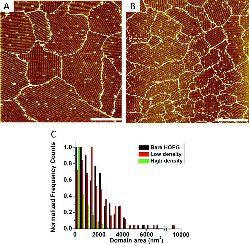 | ||
| Fig. 4 STM images of the ISA-OC18 (0.2 mM) self-assembly, at 20 °C, on modified HOPG with (A) low (Vs = −0.700 V, It = 80 pA, and scale bar = 50 nm) and (B) high densities of grafted species on the surface (Vs = −0.800 V, It = 80 pA, and scale bar = 50 nm). (C) Histogram revealing the domain size distribution of the ISA-OC18 self-assembly on bare and modified (both grafting regimes) HOPG samples, at 20 °C. | ||
The contrasting results obtained using the pristine and grafted samples need to be considered in the context of the different stages involved in 2-D crystal growth. Similar to the bulk crystallization of materials, the self-assembly of molecules at the solution–solid interface also proceeds in three distinct stages; namely, nucleation, free growth, and ripening.24 Nucleation involves the adsorption of molecules from the solution onto the surface followed by their 2-D diffusion to form small islands.
This highly dynamic process involves constant formation and dissolution of molecular islands until they reach a certain critical size above which the rate of formation is larger than the rate of dissolution. Nucleation is followed by free growth of the domains, where molecules are added to growing crystallites.
When the whole surface is covered, free growth is not possible and the domains can become larger only by consuming neighboring domains. At low temperatures, the ripening step is slow, and it is often sufficient to only consider the nucleation and free growth steps to describe the outcome of self-assembly.25 The increased number of pins, as well as the lowered distance between them (Fig. 2E) in the samples with a high grafting density, makes the arrays of pins act as barriers slowing down the domain growth (see also Section S3 in the ESI†). Consequently, new crystals nucleate on the yet uncovered substrate, eventually yielding a monolayer composed of many small domains. The results of a dedicated investigation of the nucleation of ISA-OC18 on grafted surfaces will be reported elsewhere.
Even though at a low grafting density the grafted aryls do not induce any significant alteration to the number of domains, it would be a mistake to think that the pins are inactive. They also limit the maximum size of the domains that can be grown. The only reason why this was not apparent is that at 20 °C, the domains do not grow larger even on defect-free HOPG. To support this statement, we performed experiments at 25 °C. In this case, a temperature difference of only 5 °C was enough to promote the formation of very large domains of the ISA-OC18 assemblies on bare HOPG (Fig. 5A). This is understandable since increasing the temperature simultaneously decreases the probability of nucleation and increases the rate of free growth. Yet when the same self-assembly occurred on the samples with a low grafting density, 2-D growth was limited by the defects (Fig. 5B), showing a very similar domain size distribution to the one observed on the low density grafted samples at 20 °C (see the ESI, Fig. S2†).
 | ||
| Fig. 5 (A and B) STM images of ISA-OC18 (0.2 mM) with self-assembly formed at 25 °C, on: (A) bare HOPG (Vs = −0.775 V, It = 90 pA, and scale bar = 50 nm) and (B) modified HOPG with a low density of grafted species (Vs = −0.700 V, It = 100 pA, and scale bar = 50 nm). (C and D) STM images of ISA-OC18 (0.2 mM) with self-assembly formed at 20 °C, annealed at 60 °C for 5 min and imaged after cooling back to 20 °C: (C) on modified HOPG with a low density of grafted species (Vs = −0.700 V, It = 80 pA, and scale bar = 50 nm) and (D) on modified HOPG with a high density of grafted species (Vs = −0.700 V, It = 80 pA, and scale bar = 50 nm). | ||
So far, we have seen the influence of the defects on the nucleation and growth of the ISA-OC18 assemblies. To observe the ripening of 2-D crystals we have to anneal the assembly at higher temperatures, since at ambient temperatures the ripening of these assemblies is too slow to follow with STM. For this, the assemblies formed at 20 °C were annealed for 5 minutes at 60 °C, cooled down to 20 °C and imaged. The short annealing time prevented significant solvent evaporation. The grafted aryls remain unaltered, yet significant reconstruction of the ISA-OC18 self-assembly occurred. On the samples with a low surface density of pins the domains grow very large (≥40000 nm2), with the majority of the pins being inside the domains (Fig. 5C), causing only a minor disruption of the intermolecular interactions within the isolated lamellae; as is also observed in Fig. 3A and B. Annealing the ISA-OC18 self-assembly on the samples with a high surface density of pins also resulted in the ripening of the domains (Fig. 5D). Here, however, very large domains (>40000 nm2) are rare and, instead, the domains are significantly smaller and spread in size over a rather wide range (200–15000 nm2, see ESI Fig. S3†). This is the direct consequence of the very small nearest neighbor distances (2–15 nm, Fig. 2E) between the pins in these samples and the randomness of grafting. Interestingly, the pin defects do not seem to complicate the shape of the domains – just make them smaller (see Section S6 in the ESI†). Thus, suitably grafted samples can be effectively used to slow down the growth and ripening stages in 2-D crystallization.
In addition to the ease of introduction, high control over the degree of surface modification and robustness of the defect sites, grafted aryls can be removed selectively and with nanometer precision.19 This makes arylated substrates very powerful test-beds for different experiments at the nanoscale. For example, the local removal of pins in selected areas (marked with white squares in Fig. 6A and C) results in room temperature ripening of the relevant domains only within the degrafted region (Fig. 6B and D).
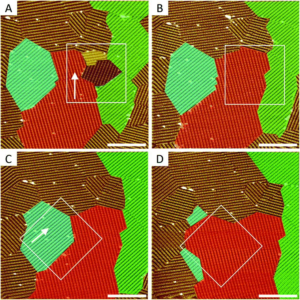 | ||
| Fig. 6 STM images of ISA-OC18 (0.2 mM) on modified HOPG with a low density of grafted species where the pins enclosed within the marked areas (white squares) of (A) and (C) were locally removed using mild STM lithography conditions (Vs = −0.001 V, and It = 200 pA). Ostwald ripening followed in the degrafted zones (B) and (D) in the next scan (Vs = −0.720 V, It = 70 pA, and scale bar = 40 nm). | ||
The reconstruction is fast and is driven by the minimization of thermodynamically unstable inter-domain borders. The outcome: large domains grow at the expense of smaller ones (Ostwald ripening). Interestingly, it appears that the sequence in which the pins are removed (for now this has only been done by controlling the scanning direction during degrafting) defines which domains will compete, and in what order. The STM precision is sufficient to remove a single pin without affecting its neighbors (see ESI, Fig. S4†). Thus, using lithographic scripts, it should be possible to program any removal sequence of designated pins. The applicability and limitations of this idea are currently under investigation.
Conclusions
We have investigated the self-assembly of 5-octadecyloxy-isophthalic acid (ISA-OC18) on arylated graphite at the liquid–solid interface. Grafted aryls (pins) act as surface defects: they locally disrupt supramolecular networks, and can alter the nucleation, growth, and ripening of 2-D crystals. The use of covalently grafted surfaces allows tuning the morphology of self-assembled monolayers, creating polycrystalline surfaces with improved thermal stability. The ability to remove defects selectively with nanometer precision was used to follow localized Ostwald ripening, triggered by in situ degrafting of selected pins. The ease of grafting, chemical robustness and selective degrafting make covalently arylated HOPG a powerful test-bed for the advanced characterization of 2-D crystallization at the nanoscale.Experimental section
Scanning tunneling microscopy
Small amounts (∼12 μL) of ISA-OC18 solutions were drop-casted onto the basal (0001) plane of freshly cleaved highly oriented pyrolytic graphite (HOPG, grade ZYB, Advanced Ceramics Inc., Cleveland, OH, U.S.A.) and visualized with scanning tunneling microscopy (STM – PicoLE (Agilent) or a Molecular Imaging STM system) in a constant current mode. The tips were mechanically cut from a Pt/Ir (80/20, ∅ 0.25 mm) wire. Several samples were investigated, and for each sample, several locations were probed. The bias voltage refers to the substrate. STM data analysis was performed using a WSxM 5.0.40 and scanning probe image processor (SPIP) software (Image Metrology ApS). High-resolution images were corrected for drift using the recorded graphite images for calibration purposes allowing a more accurate unit cell determination.Electrochemical measurements and grafting protocol
All electrochemical measurements were performed using an Autolab PGSTAT101 potentiostat (Metrohm_Autolab BV, The Netherlands). Prior to each experiment, the HOPG electrode was freshly cleaved using scotch tape. The electrochemical modification of the HOPG samples was carried out in a lab-built single-compartment three-electrode cell, with a working electrode area of 38.5 mm2, a Pt wire counter and Ag/AgCl/3 M NaCl reference electrodes. 3,5-Bis-tert-butylbenzenediazonium (3,5-TBD) is unstable, and decomposes rapidly; hence, it was synthesized from an aniline precursor immediately prior to electrochemical reduction. 3,5-Bis-tert-butylaniline (98%) was purchased from TCI-Tokyo Chemical Industry Co., Ltd. and used without further purification. 5 mL of 3,5-bis-tert-butylaniline (0.05–0.2 mM and 0.4 mM for low-density and high-density grafting, respectively) in 0.05 M HCl aq was mixed with aqueous NaNO2 (0.1 mL, 0.1 M), and after approximately 3 min the mixture was injected into an electrochemical cell to run cyclic voltammetry (3 cycles, range: 0.5 V to −0.6 V, scanning rate: 100 mV s−1). After modification, the 3,5-TBD modified HOPG samples were rinsed with Milli-Q water to remove any physisorbed material from the surface, and dried in a stream of argon. The grafting density varied both within and between samples, hence we found it more reliable to split grafting into two categories (low ρN = 1500–6000 pins per μm2 and high ρN = 13000–22000 pins per μm2) by directly analyzing the surface density of the pins in the STM images.
Acknowledgements
This work is supported by the Fund of Scientific Research – Flanders (FWO), KU Leuven Internal Funds, and the Belgian Federal Science Policy Office (IAP-7/05). The research leading to these results has also received funding from the European Research Council under the European Union's Seventh Framework Programme (FP7/2007–2013)/ERC Grant Agreement no. 340324.Notes and references
- J. A. Theobald, N. S. Oxtoby, M. A. Phillips, N. R. Champness and P. H. Beton, Nature, 2003, 424, 1029–1031 CrossRef CAS PubMed.
- Y. Xue and M. B. Zimmt, J. Am. Chem. Soc., 2012, 134, 4513–4516 CrossRef CAS PubMed.
- M. O. Blunt, J. C. Russell, M. d. C. Giménez-López, J. P. Garrahan, X. Lin, M. Schröder, N. R. Champness and P. H. Beton, Science, 2008, 322, 1077–1081 CrossRef CAS PubMed.
- J. A. A. W. Elemans, S. Lei and S. De Feyter, Angew. Chem., Int. Ed., 2009, 48, 7298–7332 CrossRef CAS PubMed.
- M. Blunt, X. Lin, M. d. C. Gimenez-Lopez, M. Schroder, N. R. Champness and P. H. Beton, Chem. Commun., 2008, 2304–2306, 10.1039/b801267a.
- S. J. H. Griessl, M. Lackinger, F. Jamitzky, T. Markert, M. Hietschold and W. M. Heckl, Langmuir, 2004, 20, 9403–9407 CrossRef CAS PubMed.
- D. Wu, K. Deng, Q. Zeng and C. Wang, J. Phys. Chem. B, 2005, 109, 22296–22300 CrossRef CAS PubMed.
- J. M. MacLeod, O. Ivasenko, C. Fu, T. Taerum, F. Rosei and D. F. Perepichka, J. Am. Chem. Soc., 2009, 131, 16844–16850 CrossRef CAS PubMed.
- D. Cahen, A. Kahn and E. Umbach, Mater. Today, 2005, 8, 32–41 CrossRef CAS.
- M. Lackinger, S. Griessl, T. Markert, F. Jamitzky and W. M. Heckl, J. Phys. Chem. B, 2004, 108, 13652–13655 CrossRef CAS.
- M. O. Blunt, J. Adisoejoso, K. Tahara, K. Katayama, M. Van der Auweraer, Y. Tobe and S. De Feyter, J. Am. Chem. Soc., 2013, 135, 12068–12075 CrossRef CAS PubMed.
- C. Marie, F. Silly, L. Tortech, K. Müllen and D. Fichou, ACS Nano, 2010, 4, 1288–1292 CrossRef CAS PubMed.
- F. Silly, J. Phys. Chem. C, 2012, 116, 10029–10032 CAS.
- W. Mamdouh, H. Uji-i, J. S. Ladislaw, A. E. Dulcey, V. Percec, F. C. De Schryver and S. De Feyter, J. Am. Chem. Soc., 2006, 128, 317–325 CrossRef CAS PubMed.
- X. Zhang, T. Chen, Q. Chen, G.-J. Deng, Q.-H. Fan and L.-J. Wan, Chem.–Eur. J., 2009, 15, 9669–9673 CrossRef CAS PubMed.
- S.-L. Lee, C.-Y. J. Chi, M.-J. Huang, C.-h. Chen, C.-W. Li, K. Pati and R.-S. Liu, J. Am. Chem. Soc., 2008, 130, 10454–10455 CrossRef CAS PubMed.
- T. Balandina, K. Tahara, N. Sändig, M. O. Blunt, J. Adisoejoso, S. Lei, F. Zerbetto, Y. Tobe and S. De Feyter, ACS Nano, 2012, 6, 8381–8389 CrossRef CAS PubMed.
- R. Addou and M. Batzill, Langmuir, 2013, 29, 6354–6360 CrossRef CAS PubMed.
- J. Greenwood, T. H. Phan, Y. Fujita, Z. Li, O. Ivasenko, W. Vanderlinden, H. Van Gorp, W. Frederickx, G. Lu, K. Tahara, Y. Tobe, H. Uji-i, S. F. L. Mertens and S. De Feyter, ACS Nano, 2015, 9, 5520–5535 CrossRef CAS PubMed.
- S. De Feyter, A. Gesquière, M. Klapper, K. Müllen and F. C. De Schryver, Nano Lett., 2003, 3, 1485–1488 CrossRef CAS.
- F. Tao and S. L. Bernasek, Surf. Sci., 2007, 601, 2284–2290 CrossRef CAS.
- P. N. Dickerson, A. M. Hibberd, N. Oncel and S. L. Bernasek, Langmuir, 2010, 26, 18155–18161 CrossRef CAS PubMed.
- K.-W. Park, J. Adisoejoso, J. Plas, J. Hong, K. Müllen and S. De Feyter, Langmuir, 2014, 30, 15206–15211 CrossRef CAS PubMed.
- K. Kim, K. E. Plass and A. J. Matzger, Langmuir, 2003, 19, 7149–7152 CrossRef CAS.
- Y. Fang, E. Ghijsens, O. Ivasenko, H. Cao, A. Noguchi, K. S. Mali, K. Tahara, Y. Tobe and S. De Feyter, Nat. Chem., 2016, 8, 711–717 CrossRef CAS PubMed.
Footnote |
| † Electronic supplementary information (ESI) available: Description of data processing; assessment of the randomness of pin placement; influence of temperature; fractal analysis; STM nanolithography. See DOI: 10.1039/c6sc02400a |
| This journal is © The Royal Society of Chemistry 2016 |