
 Open Access Article
 This Open Access Article is licensed under a Creative Commons Attribution-Non Commercial 3.0 Unported Licence
Identification of dipole disorder in low temperature solution processed oxides: its utility and suppression for transparent high performance solution-processed hybrid electronics†
Kulbinder
Banger
*a,
Christopher
Warwick‡
a,
Jiang
Lang‡
a,
Katharina
Broch‡
a,
Jonathan E.
Halpert
a,
Josephine
Socratous
a,
Adam
Brown
a,
Timothy
Leedham§
b and
Henning
Sirringhaus
*a
aOptoelectronics Group, Cavendish Laboratory, JJ Thomson Avenue, Cambridge CB3 0HE, UK. E-mail: kkb26@cam.ac.uk; hs220@cam.ac.uk
bMultivalent Ltd., Eriswell, Suffolk IP27 9BJ, UK
First published on 11th July 2016
Abstract
The ability to deposit high-quality inorganic semiconductors and dielectrics from solution at low process temperatures (∼200 °C) has become a very important research focus. During the course of our investigation, we identify the presence of an induced dipole present in solid state solution processed inorganic oxide insulator layers processed at reduced temperature (200–350 °C) from either molecular precursors, or well-dispersed metal oxide nanoparticles. Chemical composition analysis coupled with electrical measurements shows that the dielectric instability occurs due to proton migration via the Grotthuss mechanism inducing a long lived dipole disorder. Thus we established conditions for suppressing this effect to afford “ideal” high-k dielectric layer. Using this methodology, solution processed all inorganic thin film transistors (TFTs) with charge carrier mobilities exceeding 6 cm2 V−1 s−1 operating at low voltage (5 V) have been achieved. In addition, we show the broad utility of the perovskite high-k dielectric when processed with state of the art polymer and single crystal organic semiconductors yielding mobilities of approx. 7 cm2 V−1 s−1 at only 4 V. These transparent devices demonstrate excellent electrical device stability and a threshold voltage shift of only 0.41 V over 14 h, which is comparable, or better than sputtered oxide films.
Introduction
Solution processed TFTs for enabling technologies such as transparent low-temperature, large-area flexible electronics and displays have made great advances with mobilities for both organic and inorganic semiconductor devices exceeding 1–10 cm2 V−1 s−1 having been reported.1–10 However, for both types of devices, less attention has been directed to compatible, low-temperature, solution-processed gate insulating layers. Consequently, a high k dielectric material which can be coupled for use in both organic and inorganic transistors has long been sought after. In mainstream use for organic TFTs the dominant dielectric materials of choice are polymer dielectrics such as poly(methyl methacrylate) (PMMA), CYTOP™ or benzocyclobutene (BCB) due to their good film forming properties, but the tradeoff is the low intrinsic relative dielectric permittivity (εr = 1.0–3.5) and need for thick films. For low voltage operation a range of high-k gate dielectrics have been considered, including self-assembled monolayer dielectrics,11–13 ion gel-polymer electrolytes,14,15 and more recently ferroelectric materials.16 For solution processed, wide bandgap metal oxide TFTs, most studies have used thermal SiO2 or vacuum deposited SiNx as insulating layer, since the focus has been on developing solution processable semiconducting materials.17 Studies which report solution processed oxide gate insulators often employ relatively high temperature processes for the formation of the dielectric.18–22 More recently, a few groups have reported solution processed dielectric layers formed at low process temperature (<300 °C); often these studies report unexpectedly high charge carrier mobilities, significant hysteresis in the device characteristics and rarely an attempt is made to characterize device stability.23,24 Hence, there is an urgent need to understand these unexpected characteristics, instability and the device physics to enable full realization of all solution, low-temperature processed oxide TFTs.The key requirements for a high performance gate dielectric layer are a high and constant, frequency- and gate voltage-independent relative permittivity, εr, low leakage current, high breakdown field, a defect-free interface with the semiconductor layer to afford a good operational/stress stability and, ideally, the ability to be used flexibly in either top or bottom gate configurations. Ta2O5 appears a suitable choice as a high-k dielectric for solution process development, however due to its band alignment it is unable to provide sufficient charge confinement at the interface with a high bandgap oxide semiconductor and hence a passivating layer is required. Alumina, although having only a moderately high relative permittivity (εr ∼ 6–9), addresses these requirements, with the added benefit of optical transparency and suitable band edge alignment with sufficient interfacial confinement for both electrons and holes.25 In our initial reference experiments, InZnO metal oxide TFTs fabricated on alumina dielectrics grown by atomic layer deposition (ALD) exhibited excellent performance. These devices exhibited low threshold voltage shift of only 0.9 V (vs. 1.7 V for SiO2) when applying a constant current stress of 5 μA over 14 h and no distinct degradation in any of the other TFT parameters (Fig. S1 and 2†). Hence, in this study we are focusing on alumina for developing a viable solution processing route.
We have previously demonstrated a powerful materials platform for highly stable solution processed InZnO as well as quaternary oxide semiconductors using tunable molecular metal alkoxide chemistry, where due to the large built in dipole moment (Mδ+–Oδ−) these compounds have a low activation energy for oxolation to the fully formed metal oxide.1 Thus, to investigate the feasibility of utilizing the alkoxide chemistry we fabricated solution processed alumina layers from [Al(OCH(CH3)2)3]n, measured their dielectric behavior and integrated them as gate insulators into solution processed InZnO TFTs. Additionally, we also fabricated devices from metal salts to begin to probe the underlying instability mechanism often observed for fully solution processed dielectric/semiconductor junctions.
Results
Alumina metal–insulator–metal (MIM) devices with Al metal top electrodes were fabricated (with thicknesses of 84–95 nm, Tfab range 275–550 °C) and the permittivity response was recorded as a function of annealing temperature and frequency (Fig. 1a). From the inset semi-log plot, the relative permittivity values are as expected for Al2O3 (εr = 6–9) and appear reasonably stable in the frequency range of 100–10![[thin space (1/6-em)]](https://www.rsc.org/images/entities/char_2009.gif) 000 Hz which is often used to extract capacitance values of the gate dielectric for the purpose of calculating the field-effect mobility. In addition, the recorded leakage current (10 nA mm−2 at 1 mV cm−1) and break down voltage (>6 mV cm−1), (Fig. S3†) were reasonable. Working TFTs fabricated from solution processed amorphous InZnO (annealed at Tfab 275 °C)26 were then fabricated on analogously processed Al2O3 layers (Fig. 1c and S4a–c†). Dielectric layers processed at 550 °C exhibit a mobility of 1.5 cm2 V−1 s−1 at 40 V, and a conventional clockwise hysteresis between forward and reverse IV curves indicating charge trapping of electrons in the accumulation layer. This behavior is similar to that of reference devices prepared on SiO2 gate dielectrics. Surprisingly, when the dielectric fabrication temperature is reduced, there is an increase in apparent TFT mobility. We call this mobility “apparent” because it is overestimated as discussed below. As previously observed by other groups, our TFT devices with an alumina dielectric layer demonstrated what appears to be good transistor characteristics, i.e. a gate field modulated current, low leakage (<1 nA), turn on at ∼0 V, small hysteresis (∼0.2 V), sub threshold value (<0.7 V per decade), and high field effect apparent mobility of near 25 cm2 V−1 s−1 (at 1 V). We found this high “apparent” mobility to be reproducible across different devices on each substrate and between runs, in some cases mobilities up to 50–75 cm2 V−1 s−1 were observed. However, we noted that TFTs with alumina processed at reduced temperatures demonstrate an “anticlockwise” hysteresis between the forward and reverse sweep. The enhancement of apparent mobility with reduced process temperature of the dielectric is unexpected as is the change in directional hysteresis; to understand this further we began to probe the dielectric properties in more detail.
000 Hz which is often used to extract capacitance values of the gate dielectric for the purpose of calculating the field-effect mobility. In addition, the recorded leakage current (10 nA mm−2 at 1 mV cm−1) and break down voltage (>6 mV cm−1), (Fig. S3†) were reasonable. Working TFTs fabricated from solution processed amorphous InZnO (annealed at Tfab 275 °C)26 were then fabricated on analogously processed Al2O3 layers (Fig. 1c and S4a–c†). Dielectric layers processed at 550 °C exhibit a mobility of 1.5 cm2 V−1 s−1 at 40 V, and a conventional clockwise hysteresis between forward and reverse IV curves indicating charge trapping of electrons in the accumulation layer. This behavior is similar to that of reference devices prepared on SiO2 gate dielectrics. Surprisingly, when the dielectric fabrication temperature is reduced, there is an increase in apparent TFT mobility. We call this mobility “apparent” because it is overestimated as discussed below. As previously observed by other groups, our TFT devices with an alumina dielectric layer demonstrated what appears to be good transistor characteristics, i.e. a gate field modulated current, low leakage (<1 nA), turn on at ∼0 V, small hysteresis (∼0.2 V), sub threshold value (<0.7 V per decade), and high field effect apparent mobility of near 25 cm2 V−1 s−1 (at 1 V). We found this high “apparent” mobility to be reproducible across different devices on each substrate and between runs, in some cases mobilities up to 50–75 cm2 V−1 s−1 were observed. However, we noted that TFTs with alumina processed at reduced temperatures demonstrate an “anticlockwise” hysteresis between the forward and reverse sweep. The enhancement of apparent mobility with reduced process temperature of the dielectric is unexpected as is the change in directional hysteresis; to understand this further we began to probe the dielectric properties in more detail.
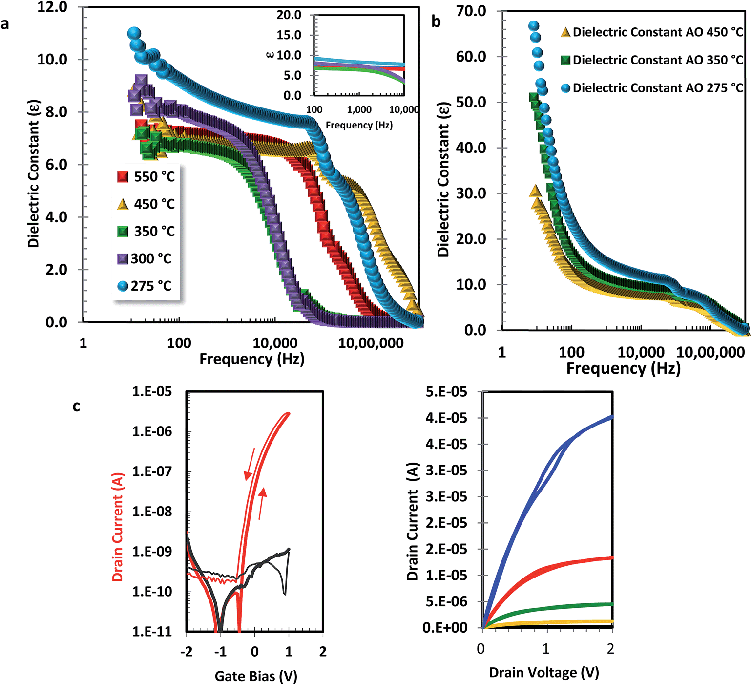 | ||
| Fig. 1 Characterization of low-temperature, solution processed alumina dielectrics: relative permittivity vs. frequency plots for solution processed alumina deposited from (a) [Al(OCH(CH3)2] and (b) Al(NO3)3 in de-ionized water (c) associated TFT transfer curve for solution processed InZnO (7:3 oxide ratio) semiconducting channel and Al2O3 gate insulating layer (deposited from [Al(OCH(CH3)2] precursor, VDS 0.1 V, W/L = 4, dielectric processing temperature 275 °C and output curve V 0–2 V, steps of 0.5 V. | ||
When examining the normalized capacitance vs. frequency (CF) response in more detail (Fig. 1a) we noticed a distinct process-temperature dependence of the low-frequency permittivity below 1 kHz. MIM devices processed at 550 °C exhibit a frequency-independent permittivity behavior. However upon reduction of the process temperature to <350 °C we begin to observe a progressive, significant increase in the permittivity at low frequencies. This is even more apparent in alumina films spin coated from an aqueous solution of AlNO3 (130–145 nm), Fig. 1b. Since the TFT device characteristics were measured in quasi-static conditions, the use of capacitance values extracted at 1 kHz (as often used in the literature), can lead to erroneous overestimation of mobility values. Thus, the apparent high mobilities of 25–75 cm2 V−1 s−1 quoted above for our low-temperature processed dielectrics are an artefact due to underestimation of the true low-frequency capacitance.
This was further confirmed when we compared the TFT transfer curves measured in pulsed mode and standard continuous mode (Fig. 2a & S4d†). During a continuous mode transfer scan the gate voltage is continuously increased from −0.5 V to +5 V and then subsequently decreased again. When taking these measurements slowly, for a total sweep time of 30–60 s, we observed a very large anticlockwise hysteresis, the device could not be turned off on the reverse scan and the ‘apparent’ extracted mobility was high. In contrast, for pulsed mode measurements a discrete gate voltage is applied to the TFT, the drain current (Id) is measured and then the gate voltage is reset to a “rest” voltage before taking another measurement at the next gate voltage. In these measurements, depending on the magnitude of “rest” voltage, the hysteresis is substantially reduced with a concomitant reduction in mobility to a more reasonable value. We confirmed that the induced dipole effect was also present in other solution processed material systems (ZrO2, HfO2), was not dependent on the specific choice of molecular precursor (organometal and non-carbon based), and was also present when using nanoparticle-based inks, supporting the fact that this was an intrinsic property (Fig. S5–7†).27
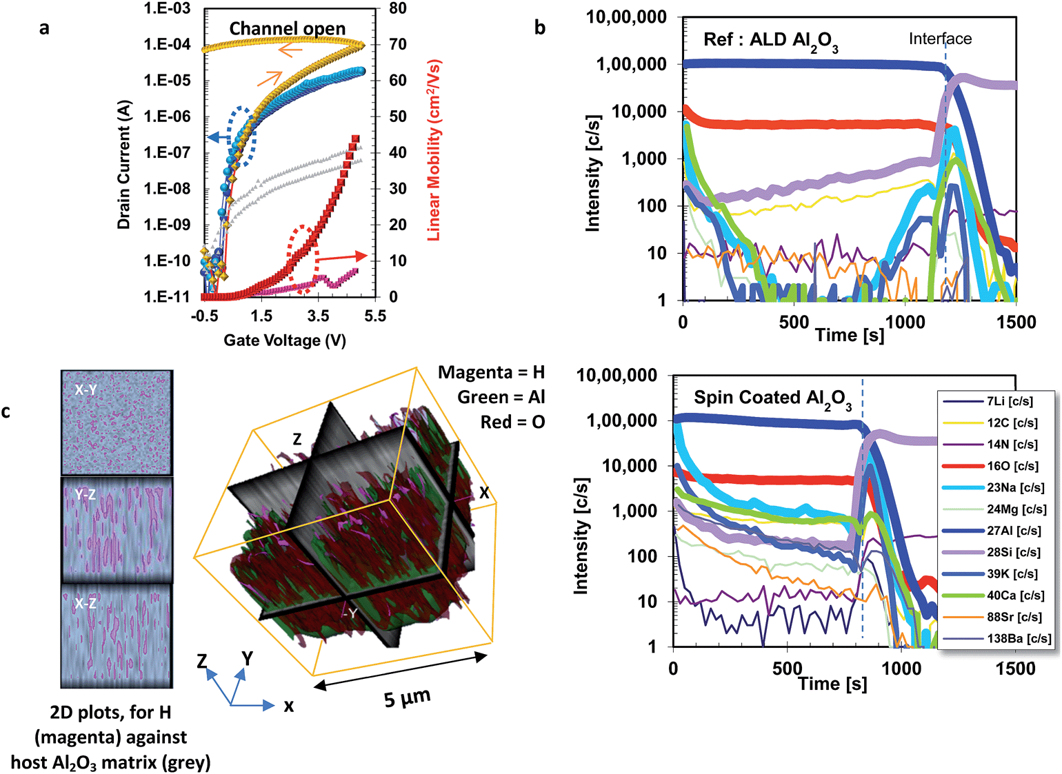 | ||
| Fig. 2 Investigation of the formation mechanism for the induced dipole in low temperature solution processed oxides: (a) overlay of transfer curves recorded in continuous mode (yellow) and pulsed mode (blue) of BGTC solution spun Al2O3/InZnO TFT on highly doped Si wafer with sputtered tungsten S/D contacts, 50 nm thick, (W = 3000 μm, L = 300 μm), (b) dynamic SIMS analysis for (top) reference Al2O3 ALD sample fabricated at 150 °C vs. (bottom) solution spun alumina from alkoxide solution processed at 250 °C. (c) 3D time-of-flight secondary-ion mass spectrometry (TOF-SIMS), for solution spun alumina showing spatial distribution of hydrogen (threshold intensity range 55–80%) against host matrix Al and O, (for clarity host opacity set to 60%); 2D plots from top front right plane, showing hydrogen (magenta) on surface (XY plane) and across the depth of the film (YZ & XZ plane) within the metal oxide host matrix (grey). | ||
Katz et al. previously reported solution-processed sodium-β-Al2O3 (SBA) dielectric layers, whereby “trapped” sodium cations within the alumina lattice would lead to extremely high capacitance.31 Dynamic-SIMS analysis indeed reveals somewhat higher concentrations of alkaline and alkaline earth impurities in our solution processed alumina vs. the reference ALD-alumina dielectric (Fig. 2b). In order to ascertain if these metal cations were responsible for the instability we fabricated films using high metal purity Al(NO3) and 2-methoxyethanol (Fig. S8†). CF measurements on MIM device structures with the high purity solution deposited alumina layer processed below 350 °C again reveals a reproducible increase in capacitance below 1 kHz. Thus ppm level metal impurities are unlikely to be fully responsible for the observed instability affect in our case. Early work on PECVD fabricated devices by Jiang et al.,32 showed that hydrogen incorporation into SiO2 gate insulator leads to TFTs with low operation voltage through diffusion of protons via a hopping mechanism. Interestingly, for solution processed oxide semiconducting thin films the incorporation of residual hydrogen is known to occur during the condensation process for –M–O–M– formation. Since we observe the induced dipole effect for oxide dielectric systems fabricated from both aqueous systems, (Fig. 1b), and also in alkoxide based, i.e. non-carbon and carbon-based, respectively, this suggests the C vs. F instability occurs from hydrogen incorporation, which can be through incomplete precursor condensation (M–OH–M).
Chemical analysis of solution processed layers
Utilizing time-of-flight secondary ion mass spectrometry (TOF-SIMS) we obtained a 3-dimensional map for hydrogen content on a 5.0 μm3 volume on our alumina films showing both lateral and depth distribution. Fig. 2c shows a graphical representation of the SIMS traces for H, Al and O, whereby the opacity for the metal oxide host matrix, which makes up the bulk of the film has been reduced by 60%, and the threshold tolerance for hydrogen is set between 55 and 80% to allow for greater clarity.33 As expected not only do we see hydrogen on the surface (X–Y 1D plot), but importantly we also detect a significant concentration of hydrogen within the bulk of the film (Y–Z, X–Z plots). To validate if the observed induced dipole occurs through a similar hydrogen doping mechanism for our films, we undertook further REELS and XPS analysis comparing our solution processed alumina layers annealed at 200–400 °C with reference ALD-Al2O3. Samples were cleaned in situ through a low energy argon sputtering step to remove any absorbed surface contributions before being probed. Modeling the XPS spectra for the O1s peak to 3 environments assignable to hydroxide species, OOH, oxygen vacancies, Ovac, and fully coordinated lattice oxygen, Olattice, at binding energies of 531, 530 & 529 eV respectively, we see a progressive increase in the hydrogen content for films fabricated at lower temperatures (Fig. S9, Table S1†). Importantly, there is also a concerted increase in the Ovac concentration, which may thus provide vacancy sites for facile hydrogen diffusion to occur.REELS analysis for our solution spun alumina films along with our reference ALD-alumina, confirm the bandgap (Eg) extracted from the onsets of band-to-band transitions, at 6.8 eV and 7.5 eV respectively, which is in good agreement with literature (Fig. S9a†).25 The primary elastic peak at 0 eV, is due to the elastically scattered electrons in contact with non-proton nuclei, whereas the much lower intensity shoulder at ∼1.8 eV is assignable to electrons elastically scattered from hydrogen atoms within the film.34 Thus the relative strength of the hydrogen related shoulder provides evidence for an increased hydrogen concentration in samples annealed at 200 °C with respect to those at 300 and 400 °C. Additionally our XPS analysis shows a decrease in the Al at% for lower annealing temperatures which suggests the formation of intrinsic cation vacancies with six nearest neighbor oxygen dangling bonds near the valence band maximum.35 For metal oxide systems, proton transport is reported to proceed through the Grotthuss mechanism involving two stages: (i) OH dipole reorientation entailing rotation of the proton around the oxygen site about the M–O–M bond vector following by (ii) proton hopping between neighboring oxygen atoms in the octahedral system, generally along the facial or meridian facets.35–38 Recent DFT calculations on amorphous Al2O3 (ref. 39) show occupancy of the bulk Alvac by intrinsic H+ where the proton sits in the electron cloud of an oxygen ion, creating a stable defect with charge ranging from q = +1 at the valence band maximum to q = −2. Thus the charge state of nearest neighbor O atoms becomes more negative with increasing formation hence increased proton binding with calculated dipole of 3.0 D.35 Additionally, experimental studies by Kroger et al. have discussed the facile diffusion of hydrogen in intrinsic defects within alumina.40 The origin of the hydrogen moiety occurs from incomplete condensation from both alkoxide precursors, however when investigating non carbon based precursors in a aqueous system, [M(OH)x]y+ we still observe the induced dipole, (Fig. 1b). Therefore, our observations support the hypothesis that the observed increase in capacitance at low frequencies in our low temperature processed gate insulators is caused primarily by the significant H concentration left in the films after the incomplete sol–gel densification process (–M–OH–M–) that leads to slow formation or reorientation of dipole moments, or the migration of protons towards the active interface when a positive gate voltage is applied.
For certain applications the formation of an induced dipole might be beneficial. For example, in some of our low-temperature solution-processed dielectric systems we have obtained preliminary evidence that the low frequency dielectric constant can reach high values potentially suitable for supercapacitor applications.28–30 However, for most electronic applications that require fast switching this induced dipole instability needs to be eliminated. For semiconducting InZnO doping with elements such as Ga which exhibit a high Gibbs energy of oxidation is a proven way to stabilize charge carrier densities through reducing the formation of oxygen vacancies, that can act as undesirable electronic dopants26,41 for TFT's and additionally for stabilization of electron transport in hybrid solar cell.42,43 Motivated by this analogy we decided to investigate doping of alumina layers with lanthanum. LaAlO3 has a high relative permittivity of εr ∼ 26 and, importantly, a similar band edge alignment with metal–oxide semiconductors as SiO2, thus likely to present a large enough potential barrier for electron confinement at the interface.
Solution processed doped alumina dielectrics
We synthesized a new La alkoxide precursor namely La2(OMIP)4Cl2, by refluxing LaCl3 in 1-methoxy-2-propanol (MIP, CH3CH(OH)CH2OCH3). Suitable crystals were grown to allow for characterization via single crystal X-ray diffraction (Fig. 3a and S10†). The precursors exist in a dimeric form bridging through the bidentate ligand, whereby a halide group resident on each metal centre has been replaced by a methoxyisopropanate ligand through a metathesis mechanism. Alumina films with increasing La doping (1.5, 3.0, 12.5 at%) were annealed and processed into MIM structures. Relative permittivity vs. frequency plots (Fig. 3b) reveal an increasing stabilization of the capacitance below 10 kHz towards a frequency independent behavior as the concentration of La doping is increased. Complete suppression of the induced dipole type behavior occurs with 12.5 at% La doping, corresponding to a clean, frequency-independent relative permittivity of 5.9 for samples processed at 250 °C. This value increases to 12 when films were annealed at higher temperatures (450 °C, Fig. S11†).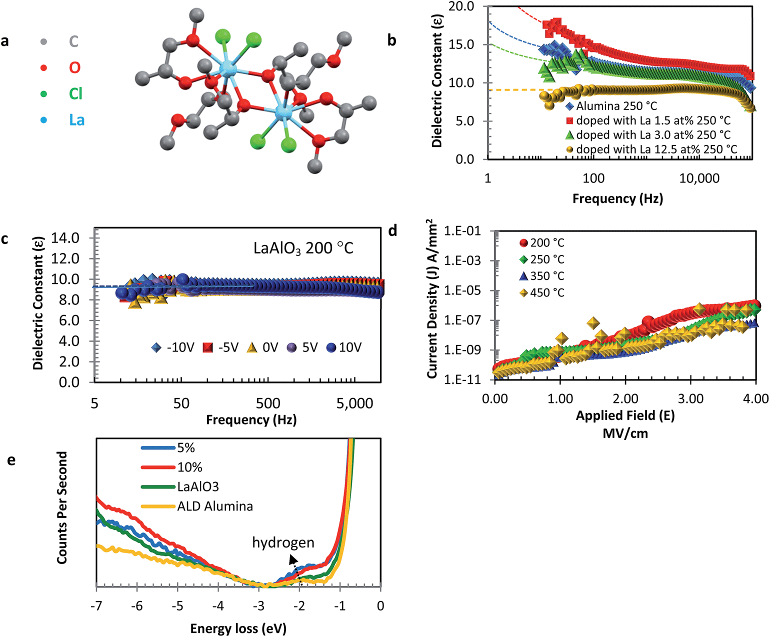 | ||
| Fig. 3 Solution processed La doped alumina dielectrics: (a) single crystal X-ray diffraction for [La2(MIP)4)Cl2] (b) dielectric constant vs. frequency plots showing stabilization of capacitance with increasing La oxide doping. (c) Dielectric constant vs. frequency plots for solution processed LaAlO3 processed at 200 °C demonstrating frequency and voltage independent dielectric response (d) leakage current plots for solution processed LaAlO3 MIM devices processed at different temperatures. (e) REELS spectra supporting reduction in hydrogen concentration with increased La doping. | ||
When the La composition is increased to reflect the LaAlO3 stoichiometry (La at% 20), capacitance vs. frequency experiments continue to show suppression of the induced dipole affect and an increase in permittivity ≥ ε = 9 for films fabricated at 200 °C with an area capacitance of 128 nF cm−2, Fig. 3c. This compares very well to the current standard reference for thermally grown, 100 nm thick SiO2 recorded at 38 nF cm−2, and with the reported high temperature (>500 °C) solution processed sodium-β-Al2O3 of 350 nF cm−2 at 1 MHz.31 Normalized plots of current density vs. applied field demonstrate excellent performance with leakage as low as 1 nA mm−2 at 2 MV cm−1 rising to only 10 nA mm−2 at 3 MV cm−1, Fig. 3d. Breakdown of our low temperature solution processed gate dielectric is observed only at >4 MV cm−1. Additionally, XRD analysis using the Bragg–Brentano configuration demonstrates that the films remain amorphous, while AFM demonstrates the layers to be atomically smooth (Fig. S12 and 13†). In order to realize fully transparent structures and to demonstrate formation on more practical substrates with higher surface roughness than silicon wafers, LaAlO3 MIM devices were also fabricated on glass at 200 °C with ITO as the bottom electrodes (sheet resistivity of 10 ohm sq−1, Fig. S14†). Devices grown on ITO show analogous behavior to those processed on highly doped SiO2 substrates. From this we can also exclude any contribution from native SiO2 to the dielectric properties when using highly doped Si wafers.
To gain insight into the “ideal” behavior observed for our solution processed LaxAlyO3 insulator, REELS and XPS spectroscopy analysis was undertaken. Fig. 3e shows normalized REELS spectra for our solution spun La-doped alumina films along with our reference ALD grown alumina. The bandgap (Eg) for Al2O3 and LaAlO3 appears at 7.5 eV and 6.6 eV respectively. The peak at 1.8 eV due to hydrogen, again, clearly shows a decrease in its areal intensity with increasing La-doping concentration consistent with the observed improvement with dielectric properties. XPS analysis of the LaAlO3 show good composition profile with peaks for La3d at 833.8 eV, Al2p 72.6 eV, and O1s at 530 eV (Fig. S15†). Modeling the O1s peak for samples with increasing La concentration we again observe a concerted decline in the area assignable to M–OH (531 eV) and M–Ovac (530 eV) with an increase in Olattice at 529 eV with increasing La concentration. We can exclude carbon content as a contributor to the instability in the dielectric films as can be seen from XPS depth profiling, Fig. S16.† For low temperature processed films (200 °C), XPS depth profiling analysis shows the presence of carbon (∼2 at%) in the bulk of film which remains independent of concentration for La doping. To exclude the contribution from carbon completely and potential contribution from Cl, LaAlO3 films were also made from a fully aqueous system (using LaNO3 and AlNO3). While the aqueous solution processed Al2O3 films from AlNO3 demonstrates CF instability, LaAlO3 demonstrates ideal dielectric behavior, Fig. S17.† Thus again reinforcing the instability is not due to carbon incorporation, but more probably due to mobile hydrogen moieties. Thus XPS analysis corroborates the REELS data. We do note the presence of a relatively small, residual percentage of H species, but as shown recently these trace amounts are unable to contribute due to trapping in perovskite structures which LaAlO3 belongs to, as recently shown by Yamazaki et al.44
Evaluation of TFT device performance and stability
To validate our low temperature high k dielectric we fabricated working transistors with binary solution processed In2O3 as semiconducting channel layer without doping due to the low thermal budget (200 °C), of the In5O(CH(CH3)2)13 precursor.26 In addition, unlike sputtered metal oxides which require doping to achieve stable devices such as IGZO, chemical derived “solution processed” indium and indium zinc oxides TFT devices have demonstrated similar electrical stability to sputter devices without the need for doping.3,4,45 Thus working TFT's were fabricated on highly doped Si substrates with our solution processed LaAlO3 dielectric layer (film thickness 92 nm).Solution processed TFTs with LaAlO3 gate insulators and In2O3 semiconducting layers processed at a maximum process temperature of 200 °C exhibits low voltage operation with maximum field effect mobilities approaching 6 cm2 V−1 s−1 at only 5 V gate bias (Fig. 4a). Importantly these devices show no anticlockwise hysteresis (<0.001 V) or scan rate dependence instability and exhibit a subthreshold swing of 0.2 V dec−1, high ON/OFF ratios ∼ 105, low onset voltage Von of −0.7 V and low gate leakage of 0.1 nA. Capacitance vs. voltage measurements on MIS structures demonstrate distinct depletion regions and full accumulation between 3 and 5 V with minimum hysteresis between forward and reverse traces (Fig. S18†). Statistical analysis for our solution processed LaAlO3/In2O3 devices were also undertaken and is shown in Fig. 4b (Fig. S19†). These demonstrate excellent uniformity within 42 TFT devices, with mobility centered on 5.0 ± 0.53 cm2 V−1 s−1, and Von at 0 V with minimum clockwise hysteresis (<0.1 V). Current stress stability measurements were carried out through application of a constant current of 3 and then 5 μA to the same device over 17 h as previously described. The shift in threshold voltage initially follows a stretched exponential behavior with ΔVth stabilizing after ∼14 h at a small value of 0.4 V and continuing to show no further degradation as recorded up to 17 h. No significant degradation was detected in any of the other TFT parameters (Fig. S20†). This is evidence for excellent operational stress stability.
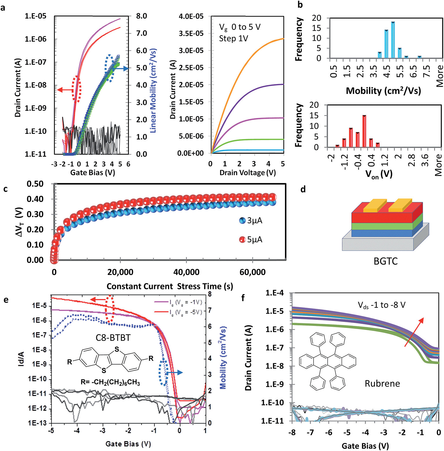 | ||
| Fig. 4 Evaluation of TFT performance, uniformity and stability: (a) output and transfer characteristics of solution-processed BGTC In2O3 TFTs with LaAlO3 gate dielectric fabricated from [Al(OIPri)3]n, [La2(OMIP)4Cl2] and In5O(CH(CH3)2)13 at a maximum processing temperature Tmax of 200 °C (VDS 0.1, 0.2 V in the transfer characteristics); (b) uniformity study across an array of 42 isolated TFT's (W/L = 10); (c) constant current stress measurements on solution processed In2O3 indium oxide solution processed channel layer with LaAlO3 dielectric with a 3 μA and 5 μA applied stress over ∼17 h, W/L = 10. (d) BGTC schematic S/D electrodes – gold, metal oxide or organic semiconductor – red, LaAlO3 – green, gate electrode – blue (e) transfer curves of hybrid BGTC TFTs with our solution processed LaAlO3 gate dielectric and polycrystalline films of C8-BTBT (W = 375 μm, L = 50 μm, left) and (f) single crystal rubrene (W = 121 μm, L = 20 μm, right). | ||
To explore the potential of our new low temperature, solution processed high-k dielectric we also investigated its use with several state-of-the-art organic semiconductors including small molecule 2,7-dioctyl[1]benzothieno[3,2-b][1]benzothiophene (C8-BTBT)6 and single crystal rubrene,46 both in bottom-gate configuration, as well as the solution processable donor–acceptor polymer, N-alkyl diketopyrrolo-pyrrole dithienylthieno[3,2-b]thiophene (DPP-DTT)47 in top-gate configuration. The transfer and output curve for the hybrid TFT's are depicted in Fig. 4d and S21.† Polycrystalline C8-BTBT was grown in a similar manner as previously reported.48 For C8-BTBT we observe ideal TFT behavior (W = 375 μm and L = 50 μm), with both linear and saturation mobilities approaching 6 cm2 V−1 s−1 at only 1 V. In the case of the TFT's with rubrene semiconducting channel layers, we again see excellent transfer characteristics. The relatively low calculated saturation mobility of 1–1.5 cm2 V−1 s−1 is due to a combination of contact resistance effects that are clearly apparent in the output characteristics (Fig. S21†) and the previously observed reduction of the mobility of rubrene in contact with high k dielectrics.46 It is remarkable that even the top-gate DPP-DTT devices functioned well, although in these structures we observed formation of some microscopic cracks in the film after the annealing of the oxide layer on top of the polymer, presumably as a result of a mismatch in the thermal expansion of the different layers (Fig. S21†).
Discussion
We have identified the presence of a slow polarisation component due to slow formation/reorientation of dipole moments in low temperature, solution processed oxide dielectrics. The induced dipole in the dielectric layer results in a frequency dependent permittivity that needs to be taken into account when extracting field-effect mobilities from low-temperature, solution-processed oxide TFTs. This also explains when these low temperature processed oxide dielectrics, when used in a TFT junction, the observed directional I–V hysteresis change from the accepted clockwise to anticlockwise due to the persistence of the induced dipole upon removal of the gate field. Chemical analysis based on dynamic-SIMS, 3D-TOF-SIMS, XPS and REELS suggests the induced dipole effect to be related to the significant hydrogen concentration remaining in low-temperature processed oxide dielectrics. Examination of LaAlO3 dielectric layers systems fabricated from both carbon and non-carbon containing precursors supports the occurrence of the instability to be precursor independent and more likely through hydrogen. We have shown that the induced dipole can be suppressed and high quality dielectrics can be realized at low process temperature (200 °C) by inclusion of a ternary element with a high Gibbs energy of oxidation, such as La. Our findings are important not only for the realization of high performance, low voltage, solution-processed oxide TFTs and the correct interpretation of their characteristics, but also more widely for the development of new low temperature functional oxide materials for a wide range of applications in optoelectronics, energy storage or energy conversion.Materials and methods
Inks/reagents/chemicals
Indium isopropoxide cluster (In5O(OCH(CH3)2)13), zinc bis methoxyethoxide (Zn(OCH2CH2OCH3)2), and La2(C24H56O12)Cl4 coordination derivatives were obtained from Multivalent Ltd (Eriswell, UK) as 0.1 M and 0.3 M parent alcohol solutions and used as received.TFT fabrication
ALD. A Beneq TFS200 system was used for depositing Al2O3 at 150 °C using Al(OPri), purchased from ABCR GmbH, and deionized water. Solution processed dielectric layers using alkoxides molecular precursors were fabricated by flooding the substrate with filtered inks (0.2 μm filters) and then spin coating under an inert, nitrogen atmosphere using a maximum spin speed of 4000 rpm and a spin time of 40 seconds. Samples were then either used as is, or subjected to a brief heating cycle at 200 °C for 5 minutes. The step was repeated for a second time and annealed for 2 h in air at designated temperatures. Reference samples from metal nitrates and oxy halides where fabricated using 0.3 M inks made by dissolving the respective salt in the desired alcohol solution or high purity water (MΩ 18) and stirred for 24 h before use. Metal oxide layers were made in an analogous manner as described above but in air. All process temperatures recorded were from surface mounted calibrated thermocouples.
Organic channel layers. BGTC organic channel layers for C8-BTBT, rubrene were fabricated as cited in the main body of text. But briefly organic layers were grown on pre-fabricated LaAlO3 processed at 200 °C. The surface energy was modified using H3PO4 as described elsewhere.49 Samples were then completed by thermal evaporation of gold source and drain contacts through a shadow mask. TGBC DPP-DTT devices; on cleaned quart substrates, photolithographically defined electrodes of Cr/Au (3 nm/18 nm) were evaporated over which DPP-DTT was spin coated from a solution of dichlorobenzene. The sample was annealed at 100 °C for 60 min. Then an ultrathin organofluorine layer (Teflon, CYTOP™) was spin coated on top and subjected to a brief heating step to remove the volatile fluorinated solvent (80 °C 30 min). LaAlO3 was then deposited on top via spin coating the metal oxide inks as described earlier and then entire stack and then annealing at 180–200 °C to facilitate densification. The device was completed by thermal evaporation of the metal gate through a shadow mask.
| μeff = ∂ID/∂VGS(W/LCoxVDS)−1 | (1) |
Acknowledgements
We dedicate this article to Dr Timothy Leedham, whose passion for alkoxide chemistry and simple belief for solving difficult problems with basic solutions remains with us after his unexpected departure. We gratefully acknowledge financial support from the European Commission through the POINTS project (FP7-NMP-2010-Small-4). K. Broch acknowledges funding by the German Research Foundation (BR 4869/1-1). We would like to thank W. Jennings (Swagelok Center for Surface Analysis of Materials, OH USA) for 3D TOF Sims, A. Chew and D. Sykes (Loughborough Surface Analysis, UK) for SIMS analysis.References
- K. K. Banger, Y. Yamashita, K. Mori, R. L. Peterson, T. Leedham, J. Rickard and H. Sirringhaus, Nat. Mater., 2011, 10, 45–50 CrossRef CAS PubMed.
- Y. Diao, B. C.-K. Tee, G. Giri, J. Xu, D. H. Kim, H. a. Becerril, R. M. Stoltenberg, T. H. Lee, G. Xue, S. C. B. Mannsfeld and Z. Bao, Nat. Mater., 2013, 12, 665–671 CrossRef CAS PubMed.
- Y. Hwan Hwang, J.-S. Seo, J. Moon Yun, H. Park, S. Yang, S.-H. Ko Park and B.-S. Bae, NPG Asia Mater., 2013, 5, e45 CrossRef.
- M. G. Kim, M. G. Kanatzidis, A. Facchetti and T. J. Marks, Nat. Mater., 2011, 10, 382–388 CrossRef CAS PubMed.
- S. T. Meyers, J. T. Anderson, C. M. Hung, J. Thompson, J. F. Wager and D. A. Keszler, J. Am. Chem. Soc., 2008, 130, 17603–17609 CrossRef CAS PubMed.
- H. Minemawari, T. Yamada, H. Matsui, J. Tsutsumi, S. Haas, R. Chiba, R. Kumai and T. Hasegawa, Nature, 2011, 475, 364–367 CrossRef CAS PubMed.
- D. Venkateshvaran, M. Nikolka, A. Sadhanala, V. Lemaur, M. Zelazny, M. Kepa, M. Hurhangee, A. J. Kronemeijer, V. Pecunia, I. Nasrallah, I. Romanov, K. Broch, I. McCulloch, D. Emin, Y. Olivier, J. Cornil, D. Beljonne and H. Sirringhaus, Nature, 2014, 515, 384–388 CrossRef CAS PubMed.
- Y. Yuan, G. Giri, A. L. Ayzner, A. P. Zoombelt, S. C. B. Mannsfeld, J. Chen, D. Nordlund, M. F. Toney, J. Huang and Z. Bao, Nat. Commun., 2014, 5, 3005 Search PubMed.
- E. Fortunato, P. Barquinha and R. Martins, Adv. Mater., 2012, 24, 2945–2986 CrossRef CAS PubMed.
- Y.-H. Kim, J.-S. Heo, T.-H. Kim, S. Park, M.-H. Yoon, J. Kim, M. S. Oh, G.-R. Yi, Y.-Y. Noh and S. K. Park, Nature, 2012, 489, 128–132 CrossRef CAS PubMed.
- H. Klauk, U. Zschieschang, J. Pflaum and M. Halik, Nature, 2007, 445, 745–748 CrossRef CAS PubMed.
- K. Everaerts, J. D. Emery, D. Jariwala, H. J. Karmel, V. K. Sangwan, P. L. Prabhumirashi, M. L. Geier, J. J. McMorrow, M. J. Bedzyk, A. Facchetti, M. C. Hersam and T. J. Marks, J. Am. Chem. Soc., 2013, 135, 8926–8939 CrossRef CAS PubMed.
- S. Thiemann, M. Gruber, I. Lokteva, J. Hirschmann, M. Halik and J. Zaumseil, ACS Appl. Mater. Interfaces, 2013, 5, 1656–1662 CAS.
- S. Wang, M. Ha, M. Manno, C. Daniel Frisbie and C. Leighton, Nat. Commun., 2012, 3, 1210 CrossRef PubMed.
- A. S. Dhoot, J. D. Yuen, M. Heeney, I. McCulloch, D. Moses and A. J. Heeger, Proc. Natl. Acad. Sci. U. S. A., 2006, 103, 11834–11837 CrossRef CAS PubMed.
- Ferroelectric Dielectrics Integrated On Silicon, ed. E. Defay, ISTE Ltd., 2011 Search PubMed.
- P. Barquinha, Transparent oxide electronics: from materials to devices, Wiley, Hoboken, NJ, 2012 Search PubMed.
- K. Jiang, J. T. Anderson, K. Hoshino, D. Li, J. F. Wager and D. A. Keszler, Chem. Mater., 2011, 23, 945–952 CrossRef CAS.
- Solution Processing of Inorganic Materials, ed. D. B. Mitzi, John Wiley & Sons, Inc., Hoboken, NJ, USA, 2008 Search PubMed.
- S. T. Meyers, J. T. Anderson, D. Hong, C. M. Hung, J. F. Wager and D. A. Keszler, Chem. Mater., 2007, 19, 4023–4029 CrossRef CAS.
- I. W. Boyd and J. Y. Zhang, Solid-State Electron., 2001, 45, 1413–1431 CrossRef CAS.
- S. Jeong, J.-Y. Lee, S. S. Lee, Y.-H. Seo, S.-Y. Kim, J.-U. Park, B.-H. Ryu, W. Yang, J. Moon and Y. Choi, J. Mater. Chem. C, 2013, 1, 4236 RSC.
- A. Liu, G. X. Liu, H. H. Zhu, F. Xu, E. Fortunato, R. Martins and F. K. Shan, ACS Appl. Mater. Interfaces, 2014, 6, 17364–17369 CAS.
- S. Y. Je, B.-G. Son, H.-G. Kim, M.-Y. Park, L.-M. Do, R. Choi and J. K. Jeong, ACS Appl. Mater. Interfaces, 2014, 6, 18693–18703 CAS.
- J. Robertson, Rep. Prog. Phys., 2006, 69, 327–396 CrossRef CAS.
- K. K. Banger, R. L. Peterson, K. Mori, Y. Yamashita, T. Leedham and H. Sirringhaus, Chem. Mater., 2014, 26, 1195–1203 CrossRef CAS PubMed.
- J. Livage, F. Beteille, C. Roux, M. Chatry and P. Davidson, Acta Mater., 1998, 46, 743–750 CrossRef CAS.
- M. F. El-Kady and R. B. Kaner, Nat. Commun., 2013, 4, 1475 CrossRef PubMed.
- Z.-S. Wu, K. Parvez, X. Feng and K. Müllen, Nat. Commun., 2013, 4, 2487 Search PubMed.
- Y. Gogotsi and P. Simon, Science, 2011, 334, 917–918 CrossRef CAS PubMed.
- B. N. Pal, B. M. Dhar, K. C. See and H. E. Katz, Nat. Mater., 2009, 8, 898–903 CrossRef CAS PubMed.
- J. Jiang, Q. Wan, J. Sun and A. Lu, Appl. Phys. Lett., 2009, 95, 152114 CrossRef.
- G. Qian, Y. Li and A. R. Gerson, Surf. Sci. Rep., 2015, 70, 86–133 CrossRef CAS.
- V. J. Rico, F. Yubero, J. P. Espinós, J. Cotrino, A. R. González-Elipe, D. Garg and S. Henry, Diamond Relat. Mater., 2007, 16, 107–111 CrossRef CAS.
- A. M. Holder, K. D. Osborn, C. J. Lobb and C. B. Musgrave, Phys. Rev. Lett., 2013, 111, 065901 CrossRef PubMed.
- R. Paul, R. Mynott, L. A. Chem, S. W. Keim, A. Chem, I. B. G.-V. Roschenthaler, W. Storzer, B. K. Kreuer and A. Rabenau, Angew. Chem., Int. Ed. Engl., 1982, 122, 1981–1982 Search PubMed.
- T. Norby, M. Widerøe, R. Glöckner and Y. Larring, 2004, 3012–3018.
- K. D. Kreuer, Annu. Rev. Mater. Res., 2003, 33, 333–359 CrossRef CAS.
- J. Martinis, K. Cooper, R. McDermott, M. Steffen, M. Ansmann, K. Osborn, K. Cicak, S. Oh, D. Pappas, R. Simmonds and C. Yu, Phys. Rev. Lett., 2005, 95, 210503 CrossRef PubMed.
- S. K. Mohapatra, S. K. Tiku and F. A. Kroger, J. Am. Ceram. Soc., 1978, 62, 50–57 CrossRef.
- J. W. Hennek, J. Smith, A. Yan, M. G. Kim, W. Zhao, V. P. Dravid, A. Facchetti and T. J. Marks, J. Am. Chem. Soc., 2013, 135, 10729–10741 CrossRef CAS PubMed.
- O. Pachoumi, C. Li, Y. Vaynzof, K. K. Banger and H. Sirringhaus, Adv. Energy Mater., 2013, 3, 1428–1436 CrossRef CAS.
- A. R. bin Mohd Yusoff, D. Kim, H. P. Kim, F. K. Shneider, W. J. da Silva and J. Jang, Energy Environ. Sci., 2014, 8, 303–316 Search PubMed.
- Y. Yamazaki, F. Blanc, Y. Okuyama, L. Buannic, J. C. Lucio-Vega, C. P. Grey and S. M. Haile, Nat. Mater., 2013, 12, 647–651 CrossRef CAS PubMed.
- Y. H. Kim, J. S. Heo, T. H. Kim, S. Park, M. H. Yoon, J. Kim, M. S. Oh, G. R. Yi, Y. Y. Noh and S. K. Park, Nature, 2012, 489, 128–191 CrossRef CAS PubMed.
- A. F. Stassen, R. W. I. de Boer, N. N. Iosad and A. F. Morpurgo, Appl. Phys. Lett., 2004, 85, 3899 CrossRef CAS.
- J. Li, Y. Zhao, H. S. Tan, Y. Guo, C.-A. Di, G. Yu, Y. Liu, M. Lin, S. H. Lim, Y. Zhou, H. Su and B. S. Ong, Sci. Rep., 2012, 2, 754 Search PubMed.
- K. Nakayama, Y. Hirose, J. Soeda, M. Yoshizumi, T. Uemura, M. Uno, W. Li, M. J. Kang, M. Yamagishi, Y. Okada, E. Miyazaki, Y. Nakazawa, A. Nakao, K. Takimiya and J. Takeya, Adv. Mater., 2011, 23, 1626–1629 CrossRef CAS PubMed.
- D. O. Hutchins, T. Weidner, J. Biao, B. Polishak, O. Acton, N. Cernetic, H. Ma and A. K.-Y. Jen, J. Mater. Chem. C, 2013, 1, 101–113 RSC.
Footnotes |
| † Electronic supplementary information (ESI) available. CCDC 1478230. For ESI and crystallographic data in CIF or other electronic format see DOI: 10.1039/c6sc01962e |
| ‡ Equal contribution. |
| § Posthumous (November 2013). |
| This journal is © The Royal Society of Chemistry 2016 |