DOI:
10.1039/C5SC03727A
(Edge Article)
Chem. Sci., 2016,
7, 1373-1382
Ultra-large optical modulation of electrochromic porous WO3 film and the local monitoring of redox activity†
Received
1st October 2015
, Accepted 11th November 2015
First published on 12th November 2015
Abstract
Porous WO3 films with ultra-high transmittance modulation were successfully fabricated on different substrates by a novel, facile and economical pulsed electrochemical deposited method with 1.1 s interval time between each pulse. The near ideal optical modulation (97.7% at 633 nm), fast switching speed (6 and 2.7 s), high coloration efficiency (118.3 cm2 C−1), and excellent cycling stability are achieved by the porous WO3 on ITO-coated glass. The outstanding electrochromic performances of the porous WO3 film were mainly attributed to the porous structure, which facilitates the charge-transfer, promotes the electrolyte infiltration and alleviates the expansion of the WO3 during H+ insertion compared to that of the compact structure. In addition, the relationships between the structural and electrochemical activity of the electrochromic WO3 films were further explored by the scanning electrochemical microscopy. These results testify that the porous structure can promote the infiltration of electrolyte and reduce the diffusion path, which consequently enhance the electrochemical activity.
1. Introduction
The decreasing availability of fossil fuels leads to the exploitation of renewable energy resources.1–3 The fraction of the world's primary energy mainly used for heating, cooling, ventilation and appliances in buildings reaches as much as 30–40%.4 Therefore, materials which are capable of converting and saving renewable energy in buildings are desirable. Electrochromic materials can reversibly change their optical properties such as transmittance, reflectance and absorption by the application of a small electric field, which is highly attractive for a wide range of potential applications, such as energy efficient smart windows, large-area information displays and antiglare automotive mirrors.5–9 Smart glass windows based on electrochromics are regarded as a very promising means of converting and saving renewable energy due to their high chromatic contrast, low cost and environmentally friendly nature, which reduces electricity consumption for cooling and decreases lighting costs by about 50% in addition to a lowered peak electricity power demand by up to 16% for commercial buildings.4
Tungsten trioxide (WO3) has been extensively investigated and identified as one of the most promising inorganic electrochromic materials.10,11 However, unsatisfactory optical modulation, long switching time and short life time limit its electrochromic effectiveness. The ideal optical modulation of electrochromic material is 100%, that is the material is fully transparent in the bleached state and fully opaque in the colored state. To date, only a few research groups have reported the optical modulation of WO3 material over 80%. Yang et al.12 reported ultrathin WO3 film exhibiting optical modulation of 76.2% at 633 nm. Cong et al.13 demonstrated the optical modulation of single-crystalline WO3 quantum dots can reach to 85% at 633 nm, but the experimental process is complex and the yield of the product is low. Recently, Liu et al.14 reported that a WO3 crystalline nanoparticle film prepared by a “nano to nano” electrodeposition approach has an optical modulation of 92% at 633 nm; however, the experimental process involved a complex two-step fabrication procedure and the switching time of the film was 9 s for coloring and 15 s for bleaching. The electrochromic phenomenon of metal oxides is attributed to the injection/extraction of electrons and ions.15–17 Nano-architectures are gaining importance in various electrochemical device applications. The nanostructures of intercalation compounds not only facilitates the electrolyte penetration and shorten the ionic diffusion paths within the electrochromic materials, but also alleviate the expansion and contraction of the host material during guest insertion and extraction. Up to now, a variety of methods have been applied to prepare nanostructured WO3 films, such as hot-filament assisted synthesis,18 sol–gel,19 sputtering,20 hydrothermal,21 solvothermal22 and electrodeposition processing.23 Among these physical and chemical fabrication techniques, electrochemical deposition methods are of particular interest due to their low cost, feasibility for large area film growth, and no requirement for further thermal treatment. In addition, various conductive substrates can be used with this deposition technique, such as conductive glass and flexible or stretchable conductive polymer substrates. Especially, flexible substrates have recently attracted great interest due to portable and highly integrated devices which need to be small size, lightweight and compliant on highly flexible substrates.24–26 Continuous and pulsed electrochemical deposited WO3 films have been demonstrated using deposition solutions prepared by dissolving sodium tungstate in dilute acid or tungsten powder in hydrogen peroxide (H2O2).27–29 However, none of these WO3 films exhibited satisfactory electrochromic performance. Therefore, it is of great importance to unravel the interdependence of desirable electrochromic behavior and material structures.
In the past, electrochemical characterizations for electrochromic materials have mostly been done on macroscopic or device level, which provide the average measurement across the interfaces. However, localized studies on the charge transport process and on electrochemical reaction are less investigated.30,31 A deeper understanding of local electrochemical properties of electrochromic materials will be beneficial to establish relationships between structural design and electrochemical activity for enhanced electrochromic performance. Scanning electrochemical microscopy (SECM) has been very successful in this respect and used for providing insightful electrochemical characterization on sub-micrometer scale investigation of a wide range of materials and interfaces.32,33 We have previously introduced SECM measurements to probe the localized interfacial kinetics at the interface of electrolyte/electrode and extract the effective heterogeneous charge transfer rate constant based on polyaniline and MnO2 for supercapacitor application.34,35
Herein, a novel, facile and economical pulsed electrochemical deposition with defined interval time between each pulse for porous WO3 film deposition is demonstrated. The porous WO3 films were fabricated on different conductive substrates without any template and no further thermal treatment is required. Electrochemical and electrochromic properties of the porous WO3 film were evaluated in this paper. The porous WO3 film exhibits excellent electrochromic performance, including near theoretical optical modulation, fast switching speed, high coloration efficiency and good cycling stability. In addition, the localized charge transport process and electrochemical reaction were investigated by in situ SECM technique to provide in-depth insights on the relationship between microcosmic structural and macroscopic electrochromic performance.
2. Experimental
2.1 Chemicals
Sodium tungstate dihydrate (Na2WO4·2H2O, ≥99%) and perchloric acid (HClO4, 70%) were purchased from Sigma-Aldrich. H2O2 (30%) was obtained from VWR International Ltd. All the chemicals were used without further purification and all aqueous solutions were prepared from deionized water (Milli-Q, Millipore Corp.).
2.2 Preparation of porous WO3 film
The deposition electrolyte solution was prepared by dissolving 1.03 g Na2WO4·2H2O in 250 ml deionized water, and then 2 ml perchloric acid and 0.65 ml H2O2 was added to the above solution under magnetic stirring. Indium tin oxide (ITO)-coated glass, fluorine-doped tin oxide (FTO)-coated glass and ITO-coated polyethylene terephthalate (PET) were used as transparent electrodes. These electrodes were first cleaned with deionized water and ethanol, and then were treated by argon plasma. The pulsed electrodeposition with 1.1 s interval time between each pulse was performed with a Solartron 1470E electrochemical workstation (Farnborough, U.K.) at room temperature using a conventional three-electrode system. The counter electrode was a 2 × 2 cm2 platinum foil and the reference electrode was an Ag/AgCl electrode. Pulsed voltages were switched between −0.7 to 0 V. Square waveform pulses were applied with a duty cycle length of 0.2 s. For one deposition cycle, a square waveform pulse at −0.7 V was first applied onto the cell for 0.1 s, followed by another square waveform pulse at 0 V which was applied to the cell for 0.1 s. Between each deposition cycle, there is a pause of 1.1 s. A whole deposition procedure involves 6000 cycles, with a total deposition time around 7800 s. After deposition, the films were thoroughly washed with methanol and water and finally dried in air. For comparison, WO3 films on ITO-glass substrates deposited by continuous electrodeposition and pulse deposition with no interval pause time were also prepared.
2.3 Sample characteristics
The morphology, structure and composition of the WO3 films were characterized by scanning electron microscopy (SEM, JEOL 7600F, Tokyo, Japan), transmission electron microscopy (TEM, JEOL 2010), and X-ray diffraction (XRD, Shimadzu diffractometer with Cu-Kα-radiation (λ = 1.5406 Å)). A Renishaw Raman microscopy is used to identify Raman spectra conducted using with a charge coupled device array detector at 532 nm laser line. The Raman signals were dispersed by 2400 line mm−1 gratings with a frequency resolution of ∼0.8 cm−1 and collected by a Leica 100× objective lens (NA = 0.85). The surface analysis of the sample was carried out using a VG ESCALab 220i-XL Imaging X-ray photoelectron spectroscope (XPS) last calibrated in Sep 2014. Monochromatic Al-Kα X-rays (hν = 1486.7 eV) were employed using a large area lens mode for analysis with photoelectron take-off angle of 90° with respect to the surface plane. The maximum analysis depth lies in the range of 4–8 nm. The charge correction is based on C![[thin space (1/6-em)]](https://www.rsc.org/images/entities/char_2009.gif) 1s of adventitious carbon at 285.0 eV. For chemical state analysis, a spectral deconvolution was performed by a curve-fitting procedure based on Lorentzians broadened by a Gaussian using the manufacturer's standard software. The error of binding energy is estimated to be within ±0.2 eV.
1s of adventitious carbon at 285.0 eV. For chemical state analysis, a spectral deconvolution was performed by a curve-fitting procedure based on Lorentzians broadened by a Gaussian using the manufacturer's standard software. The error of binding energy is estimated to be within ±0.2 eV.
2.4 Electrochemical characterization
The electrochemical and electrochromic measurements were conducted in a three-electrode electrochemical cell containing 0.5 M H2SO4 aqueous solution as the electrolyte. The voltage supply was from Solartron 1470E. The transmission spectra of WO3 films under different potentials were measured in situ over the wavelength range from 300 to 900 nm by combination of a SHIMADZU UV-3600 spectrophotometer and Solartron 1470E electrochemical workstation. The test WO3 films were used as working electrode, Ag wire was used as the reference electrode and a Pt wire was used as the counter electrode. The transmittance of the conductive substrates in the electrolyte was considered to be 100% and was used as the baseline. Cyclic voltammograms (CVs) and electrochemical impedance spectrum (EIS) tests were also conducted on the Solartron 1470 with Ag/AgCl as the reference electrode in both electrochemical measurements. SECM studies were performed on a home-built instrument running with the xyz-positioning system and bipotentiostat (Sensolytics GmbH, Germany) in a four-electrode configuration with a Pt microelectrode as working electrode 1 (WE1, rT = 12.5 μm, RG = rglass/rT = 7; rglass and rT are the radius of the glass sheath and the WE1, respectively), the WO3 film as WE2, a Pt wire as auxiliary electrode, and an Ag/AgCl reference electrode. All electrodes were immersed into 1 mM [Ru(NH3)6]Cl3 in 0.1 M KCl. SECM feedback mode approach curves were acquired through SECMx software. The WE1 current and WE1–WO3 distance during the approach curve measurements were normalized to the steady-state current and the WE1 radius, respectively, using IT = iT/iT,∞ and L = d/rT, where iT and iT,∞ are the probe current and the probe current measured far from the substrate, and d refers to tip–substrate separation distance in SECM. The normalized approach curves ITvs. L were then fitted to the analytical approximation of Cornut and Lefrou36 to obtain the normalized heterogeneous rate constant κ.
3. Results and discussion
3.1 Microstructure characteristics
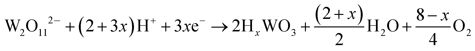
The current–time responses and corresponding SEM images of the WO3 film on ITO-coated glass are shown in Fig. 1. Uniform granules and compact smooth surface are observed in the films prepared by continuous and pulsed electrodeposition without interval time, as shown in Fig. 1b and d, which are similar to that reported by previous literatures.27–29 The size of the granules prepared by continuous electrodeposition is about 15 nm, but the size of the granules formed without interval time pulsed electrodeposition is about 30 nm, which is larger than that of the continuous electrodeposition. However, the WO3 film exhibits a porous and nanoscale interconnecting network structure when an interval time of 1.1 s is present between each pulse (Fig. 1f). The nanoscale interconnecting network is made up of flaky WO3 particles with thicknesses of about 25 nm. It is worth noting that during the interval pause time, the deposition cell was under a positive open circuit potential of 0.63 V (Fig. 1e). The mechanism of the electrodeposition can be illustrated as follows: the dimeric peroxytungstate [(O2)2W(O)·O·W(O)(O2)2]2−(W2O112−), tungsten is in a +VI oxidation state and (O2) denotes a peroxide ligand which is formed in deposition electrolytes by dissolving Na2WO4 into acidic H2O2 solutions, which undergoes a reduction and gives rise to tungsten trioxide and molecular oxygen during the electrodeposition procedure.37,38 The reaction can be described as follows:| | | 2WO42− + 4H2O2 → W2O112− + 2OH− + 3H2O | (1) |
| |  | (2) |
| | | HxWO3 → WO3 + xH+ + xe− | (3) |
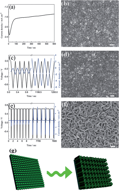 |
| | Fig. 1 The current–time responses and the corresponding SEM images for electrodeposited WO3 films on ITO glasses: (a and b) continuous deposition, (c and d) pulsed electrodeposition without interval time, (e and f) pulsed electrodeposition with 1.1 s interval time between each pulse. (g) The formation process of porous and interconnecting flaky WO3 film. | |
The film exhibits a blue color during the electrodeposition procedure, mainly due to reduced HxWO3 and exhibits metallic properties.39 The formation of HxWO3 is evident from the gradual increase in current density in Fig. 1c. The color gradually fades when the open circuit voltage arises to positive potential after electrodeposition and WO3 is formed. On the basis of the mechanism mentioned above, a model for the electrodeposited WO3 film is proposed. During the continuous cathodic electrodeposition procedure, due to the uniform electric field distribution on the surface of the substrates and the electrostatic repulsion between the negative surface charge and the negative ions, the nucleation occurs simultaneously over the entire substrate surface. Therefore, the film prepared by continuous electrodeposition is comprised of small granules. However, HxWO3 deposits are nucleated as hemispherical islands on the substrates during the pulsed electrodeposition, and the electric field is locally enhanced by the aspect ratio of the islands. Like a lightning-rod effect, the electric field lines concentrate on the convexity of a lightning conductor.40,41 New HxWO3 nuclei are formed near the tip by the overpotential, hence the size of the granules prepared by pulsed electrodeposition is larger than that of the granules prepared by continuous electrodeposition. When there is an interval time between each pulsed electrodeposition and the open circuit potential is positive during the interval time, the surface of the HxWO3 nuclei is charged positively during the interval time. A positive surface charge is preferred for the growth of HxWO3 nuclei because of the electrostatic attraction between the positive surface charge and the negative ions. With the combination of positive surface charge and lightning-rod effect, the granules interlace with one another to form a porous flaky structure. Simultaneously, the newly nucleated small islands around the flakes are dissolving under the positive potential and form the porous and nanoscale interconnecting network structure.
The model of the electrodeposition is further confirmed by changing the length of pulsed time and interval time as shown in Fig. S1 and S2 in ESI.† When the fixed interval time was 1.1 s between each pulsed electrodeposition cycle, short nano-chains are observed in the film prepared with an applied duty cycle length of 4 s (Fig. S1a†). The nano-chain is made up of small granules and the length is 50–80 nm. The length of the nano-chain is longer when the length of duty cycle decreases to 1 s (Fig. S1b†), and some porous and flaky network structure appeared in the film prepared with an applied duty cycle length of 0.5 s (Fig. S1c†). When the duty cycle length is fixed for 0.2 s, some flaky structure are observed in the film prepared by applied 0.4 s interval time between each pulsed electrodeposition cycle (Fig. S2a†). With increasing the duty cycle length, there is more positive charge gathered on the surface of the working electrode and this leads to more flaky structures interconnected with each other (Fig. S2b and c†). Therefore, the porous and interconnecting flaky WO3 film can only be formed by pulsed deposition under shorter duty cycle length and longer interval time. Fig. 1g summarizes the formation process of porous and interconnecting flaky WO3 film. Moreover, the porous and interconnecting flaky WO3 film can be deposited not only on the ITO glass, but also on FTO glass and ITO-coated PET flexible substrate as shown in Fig. S3.† This illustrates that this method has wide applications on various conductive substrates.
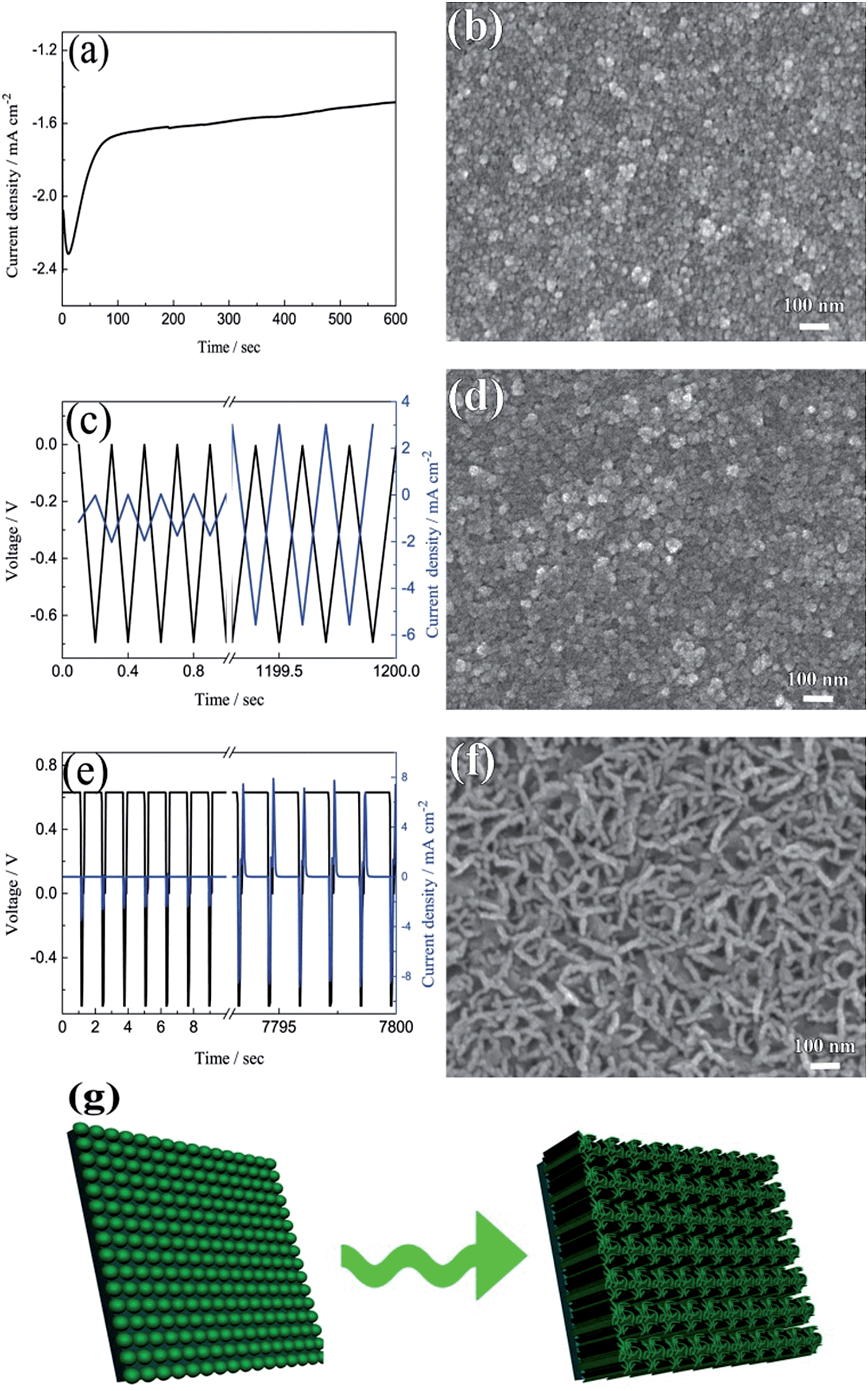
Fig. 2a shows the Raman spectra of the WO3 films. Typically, all the films exhibit a broad peak centered at 670 cm−1 resulting from the W–O stretching vibrations and a relatively sharp peak at 957 cm−1 resulting from the W![[double bond, length as m-dash]](https://www.rsc.org/images/entities/char_e001.gif) O stretching mode of terminal oxygen atoms. In addition, there is a weak and broad peak at 202 cm−1 ascribed to W–O bending vibration. These results match well with those reported in the literature for WO3.42–44 Another weaker and broad peak located around 1092 cm−1 arises due to the ITO substrate.45 The XRD pattern of the film on ITO substrate is presented in Fig. 2b. There is only an additional broadened peak display around 2θ ≈ 26.4° after subtracting the diffraction peaks of ITO glass, indicating the presence of amorphous WO3. The result is in accordance with the previous reports.46,47 XPS measurements were performed to further investigate the chemical composition and oxidation state of the films. The XPS survey spectra of the porous WO3 film only contains W, O and C as shown in Fig. 2c. Fig. 2d shows the high-resolution XPS spectrum of the W4f peak. There are spin–orbit doublets in this spectrum corresponding to W4f7/2, W4f5/2 and W5p3/2 peaks which are located at 35.9, 38.0 and 41.5 eV, respectively. These values are consistent with those reported in the literature for WO3.48,49 In addition, the ratio of O to W is 3.0 as shown in Table S1 in ESI.† It can be reasoned that W in the films is at the highest +VI oxidation state. The structural characteristics of the porous WO3 film prepared by pulsed electrodeposition with 1.1 s interval time between each cycle was further investigated by TEM, as shown in Fig. 2e and f. From the low magnification image, the WO3 film exhibits flaky structures. HRTEM and selected area electronic diffraction (SAED) results confirm that most of the film exhibits an amorphous structure. However, areas with low-range order in a few nanometers scale are observed in the HRTEM image, manifesting that there are some nanocrystals dispersed in the amorphous matrix. It is well known that the electrochromic performance of inorganic materials is closely related to its degree of crystallization.50–52 For example, crystalline WO3 film exhibited inferior electrochromic performance (such as coloration efficiency, optical modulation and switching time) compared to an amorphous one. Nevertheless, the amorphous WO3 has poorer cyclic stability.51,52 Therefore, the formation of WO3 nanocrystals is anticipated to be an integrated approach to improve the electrochromic performance of the WO3 films.
O stretching mode of terminal oxygen atoms. In addition, there is a weak and broad peak at 202 cm−1 ascribed to W–O bending vibration. These results match well with those reported in the literature for WO3.42–44 Another weaker and broad peak located around 1092 cm−1 arises due to the ITO substrate.45 The XRD pattern of the film on ITO substrate is presented in Fig. 2b. There is only an additional broadened peak display around 2θ ≈ 26.4° after subtracting the diffraction peaks of ITO glass, indicating the presence of amorphous WO3. The result is in accordance with the previous reports.46,47 XPS measurements were performed to further investigate the chemical composition and oxidation state of the films. The XPS survey spectra of the porous WO3 film only contains W, O and C as shown in Fig. 2c. Fig. 2d shows the high-resolution XPS spectrum of the W4f peak. There are spin–orbit doublets in this spectrum corresponding to W4f7/2, W4f5/2 and W5p3/2 peaks which are located at 35.9, 38.0 and 41.5 eV, respectively. These values are consistent with those reported in the literature for WO3.48,49 In addition, the ratio of O to W is 3.0 as shown in Table S1 in ESI.† It can be reasoned that W in the films is at the highest +VI oxidation state. The structural characteristics of the porous WO3 film prepared by pulsed electrodeposition with 1.1 s interval time between each cycle was further investigated by TEM, as shown in Fig. 2e and f. From the low magnification image, the WO3 film exhibits flaky structures. HRTEM and selected area electronic diffraction (SAED) results confirm that most of the film exhibits an amorphous structure. However, areas with low-range order in a few nanometers scale are observed in the HRTEM image, manifesting that there are some nanocrystals dispersed in the amorphous matrix. It is well known that the electrochromic performance of inorganic materials is closely related to its degree of crystallization.50–52 For example, crystalline WO3 film exhibited inferior electrochromic performance (such as coloration efficiency, optical modulation and switching time) compared to an amorphous one. Nevertheless, the amorphous WO3 has poorer cyclic stability.51,52 Therefore, the formation of WO3 nanocrystals is anticipated to be an integrated approach to improve the electrochromic performance of the WO3 films.
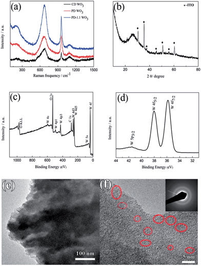 |
| | Fig. 2 (a) Raman spectra of the WO3 films, CD WO3 corresponds to the WO3 film prepared by continuous deposition, PD WO3 corresponds to the WO3 film prepared by pulsed electrodeposition without interval time, PD-1.1 WO3 corresponds to the WO3 film prepared by pulsed electrodeposition with 1.1 s interval time between each pulse. (b) XRD pattern of the WO3 film prepared by continuous deposition. (c and d) XPS survey spectra and detail of the W4f peak for the porous WO3 film. (e and f) TEM images of WO3 scratched from the WO3 film on ITO substrate prepared by pulsed electrodeposition with 1.1 s interval time between each pulse (SAED pattern presented in inset). | |
3.2 Electrochemical and electrochromic performance evaluations
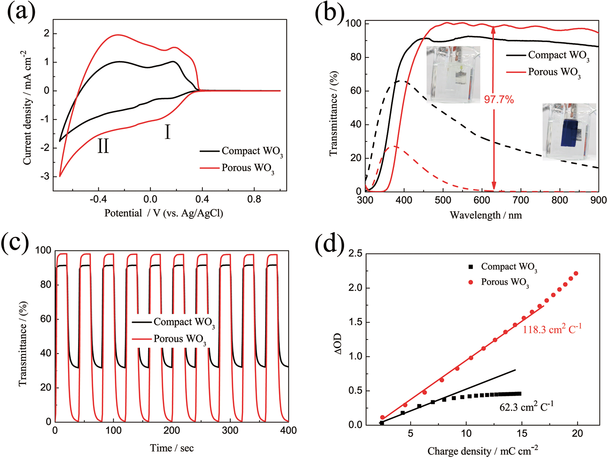
In order to evaluate the electrochemical and electrochromic performances, representative compact and porous WO3 films with thickness of about 480 nm (Fig. S4†) prepared by continuous and pulsed electrodeposition with 1.1 s interval time between each pulse were chosen. Fig. 3a shows the CVs of WO3 films carried out in the potential region of −0.7 to 1.0 V (vs. Ag/AgCl) at a scan rate of 20 mV s−1. The presence of two waves in both CV curves, denoted I and II, is attributed to the insertion of two distinct proton species: hydrated H+ ions absorbed onto WO3 surface or enclosed into pores of the oxide, and hydrated H+ ions coming from the bulk solution, respectively.53 Therefore, the recorded current is due to the H+ ion intercalation/extraction according to the reaction| | | WO3 + xH+ + xe− ↔ HxWO3 | (4) |
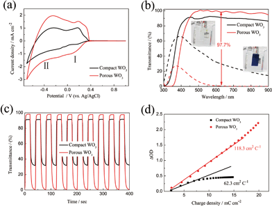 |
| | Fig. 3 (a) Cyclic voltammograms of WO3 films on ITO glass as working electrodes in 0.5 M H2SO4 at a scan rate of 20 mV s−1 in the potential range of −0.7 to 1 V vs. Ag/AgCl. (b) Transmittance spectra of the WO3 films on ITO glass in the colored (−0.7 V) and bleached (1 V) states between the wavelength range of 300 and 900 nm. (c) In situ optical responses of WO3 films on ITO glass for 20 s per step measured at 633 nm. (d) Optical density variation with respect to the charge density. | |
The potentials of the redox peaks show no significant difference for both films. However, the cathodic and anodic peak currents of the porous film are much higher than those of the compact film. These indicate that the porous WO3 film has higher electrochemical activity associated with better electrochromic properties. In order to quantitatively compare the electrochromic performances of the compact and porous WO3 films, the transmittance spectra in colored and bleached states were measured under an applied potential of −0.7 and 1.0 V, respectively, as shown in Fig. 3b. The color of the WO3 films changes from dark blue (colored state) to transparent (bleached state) reversibly. It can be seen that the porous WO3 film exhibits an ultra-large transmittance modulation reaching about 97.7% at 633 nm, the highest value for WO3 so far, to the best of our knowledge,12–14,54–56 and it is much larger than that of the compact WO3 film (61.5% at 633 nm). The digital photos of the porous WO3 film in bleached and colored state are shown in the inset of Fig. 3b. The coloration and bleaching speed of the WO3 films were investigated by chronoamperometry (CA) and the corresponding in situ transmittance at 633 nm, is as shown in Fig. 3c. The switching time is defined as the time required for a system to reach 90% of its full modulation. For the porous WO3 film, the switching time for coloration and bleaching is 6 and 2.7 s respectively, which is comparable to the compact WO3 film (6.9 and 1.9 s). However, the switching time of the porous WO3 film is much shorter than that of the compact WO3 film to reach the same transmittance modulation. In comparison with many nanostructured WO3 electrochromic materials, the switching speed of porous WO3 reported in this work is much faster than that of WO3 nanorolls (9 and 8 s),57 WO3 nanorods (272 and 364 s)58 and WO3 nanosheets (21 and 8 s).59 One of the most important criteria often used to characterize an electrochromic material is its coloration efficiency (CE). CE is defined as the change in optical density (ΔOD) per unit of charge (ΔQ) inserted into (or extracted from) the electrochromic layers. It can be calculated from the following formulas:60
| |  | (5) |
| |  | (6) |
where
Tb and
Tc refers to the transmittance in bleached and colored states, respectively. Generally, a high value of CE indicates that the electrochromic material exhibits a large optical modulation with a small intercalated (or extracted) charge density. The plots of OD at a wavelength of 633 nm as a function of inserted charge density at a potential of −0.7 V is shown in
Fig. 3d, the CE can be calculated from the slope of the curves. The CE value is calculated to be 118 cm
2 C
−1 at 633 nm for the porous WO
3 film, which is higher than that of the compact WO
3 film. The CE value of 118 cm
2 C
−1 is also higher than that of previous reported WO
3 nanomaterials, which are typically lower than 100 cm
2 C
−1.
61–63
As we know, the optical modulation and the switching time of the electrochromic material are closely related to the applied potential. However, there are very few dedicated studies to this phenomenon. Fig. 4a shows the transmittance spectra of the porous WO3 film as a function of applied potential. The transmittance spectra of the porous WO3 film at 633 nm with respect to the applied potential is depicted in Table 1. It can be seen that the porous WO3 film exhibits almost the same transmittance when the applied potential extends over 0.1 V, however, it is clear that the transmittance gradually decreases as the applied potential goes more negative. Meantime, the optical modulation gradually increases. Noticeably, our porous WO3 film exhibits an optical modulation of about 82.9% at 633 nm by applying a narrow voltage window between 0.1 and −0.4 V, and exhibits an optical modulation of about 93% at 633 nm by applying a voltage window between 0.1 and −0.5 V. To the best of our knowledge, the new porous WO3 film herein is among the best in documented inorganic materials. The switching time and the in situ transmittance at 633 nm were also recorded with respect to the applied potential as shown in Fig. 4b and c and Table 1. When the bleaching potential is fixed as 0.3 V, the optical modulation gradually increases and colored switching time gradually decreases as the applied potential goes more negative. When the colored potential is fixed as −0.7 V, the film can fully beached only when the applied potential is over 0.1 V, and the bleached switching time gradually decreases as the applied potential goes more positive. The results indicate that both large optical modulation and fast switching require a wide applied voltage window. The electrochromic phenomenon of WO3 is attributed to the injection/extraction of electrons and ions as shown in eqn (4). The colored and bleached processes correspond to H+ ion intercalation and extraction processes from the WO3 material, respectively. Therefore, more negative potential applied on the film accompanied with insertion of more H+ into WO3 material leads to reduction of W6+ ions to lower valence states and darker blue colour is observed till colour saturation, and vice versa. In addition, a larger potential means higher driven force for intercalation and extraction of H+ ion which can improve the speed of the H+ ion intercalation and extraction from the WO3 material. Hence both large optical modulation and fast switching require a wider voltage window. Usually, the voltage window of −1.0–1.0 V is applied for WO3 electrochromic materials in H2SO4 or lithium perchlorate (LiClO4) in propylene carbonate.64–67 A wider voltage window will accelerate the dissolution of WO3 dissolved in the electrolyte and affect the service life. Fig. 4d shows coloration–bleaching cycles of the compact and porous WO3 films by applying a voltage window switched between −0.7 and 0.7 V with one cycle length for 20 s. The test was conducted within 6000 s (300 switching cycles). The transmittance modulation of the compact WO3 film gradually decreases during the cycling process, and only sustains a transmittance modulation of about 52.4% of its initial value after subjected for 3000 s. By contrast, almost no change of the transmittance modulation of the porous WO3 film was observed over 6000 s. The stability of the porous WO3 film is also better than that of the single-crystalline WO3 quantum dots13 and thiourea-assisted prepared nanostructured WO3,68 in which degradation was observed just after 50 repeated switching cycles. These results indicate that the porous WO3 film possesses reasonably good cycling durability. The improved electrochromic properties of the porous WO3 film are mainly attributed to the porous structure, which facilitates the charge-transfer and alleviates the expansion of the WO3 material during H+ insertion.69–71 To further understand the electrochemical behavior of the compact and porous WO3 films, a nondestructive and sensitive technique, EIS, was conducted in a frequency range of 100 kHz to 0.1 Hz at open-circuit potential. Fig. S5† shows the Nyquist plots of the compact and porous WO3 films; the intercept at the real axis (Z′) contains the intrinsic resistance of the substrate, electrolyte resistance, and the contact resistance between active material and substrate. In addition, both EIS spectra consist of a semicircle in the high-frequency region and a straight line in the low-frequency region. The semicircle is related to the charge transfer impedance and the straight line is ascribed to the diffusion-controlled Warburg impedance.72–75 Obviously, the porous WO3 film exhibits a lower intercept at the real axis and a smaller semicircle in the high frequency region, indicating smaller contact resistance and charger transfer resistance compared to that of the compact WO3 film.
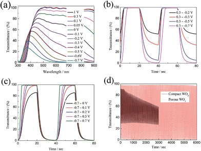 |
| | Fig. 4 (a) Transmittance of porous WO3 film as a function of applied potential. (b and c) In situ optical responses of porous WO3 films measured at 633 nm as a function of applied potential. (d) Cycle performance of the WO3 films measured in 0.5 M H2SO4 for 6000 s. | |
Table 1 Various parameters of porous WO3 film as a function of applied potential
| Applied voltage (V) |
Transmittance (%) at 633 nm |
Applied voltage window |
Switching time (s) |
| 1.0 |
98.184 |
0.3 to −0.2 |
t
c = 10.0 |
| 0.3 |
98.757 |
0.3 to −0.3 |
t
c = 9.8 |
| 0.1 |
98.317 |
0.3 to −0.5 |
t
c = 9.0 |
| 0.05 |
93.483 |
0.3 to −0.7 |
t
c = 6.0 |
| 0 |
85.833 |
−0.7 to 0 |
t
b = 11.6 |
| −0.1 |
70.173 |
−0.7 to 0.1 |
t
b = 10.2 |
| −0.2 |
52.129 |
−0.7 to 0.2 |
t
b = 8.0 |
| −0.3 |
32.76 |
−0.7 to 0.3 |
t
b = 6.5 |
| −0.4 |
15.426 |
−0.7 to 0.7 |
t
b = 3.6 |
| −0.5 |
5.222 |
−0.7 to 1.0 |
t
b = 2.7 |
| −0.6 |
1.470 |
— |
— |
| −0.7 |
0.495 |
— |
— |
The large optical modulation and fast switching speed of the porous WO3 were not only observed on the ITO substrate, but could also be achieved on FTO-coated glass and ITO-coated PET flexible substrate as shown in Fig. 5. The porous WO3 films deposited on FTO glass and ITO-coated PET flexible substrate exhibit an optical modulation of 93.8 and 96.6% at 633 nm, respectively. The colored/bleached switching time of the WO3 deposited on FTO glass and ITO-coated PET flexible substrate are 9.2/4.6 and 14/6.6 s, respectively. The digital photos of the porous WO3 at bleached and colored state are shown in the corresponding inset of Fig. 5a and c. The results indicated good electrochromic performance can obtained on various transparent conductive substrates.
 |
| | Fig. 5 Transmittance spectra and in situ optical responses of the WO3 films on different substrates between the colored and bleached states; (a and b) FTO substrate, (c and d) ITO-PET substrate. | |
3.3 Local visualization of redox activity by SECM
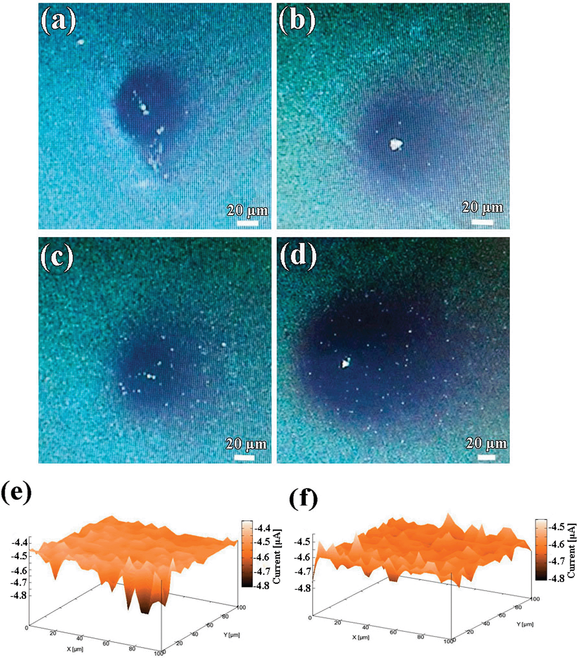
In order to further understand the relationships between the structural and electrochemical activity of the electrochromic material, local electrochemistry of the electrode materials was studied using SECM. SECM has been considered as an essential tool to study not only the local electrochemical activity of the surface at micrometric scales, but also to evaluate local topographical characteristics of the scanned area. In the typical SECM measurement, the localized CVs of WE1 were carried out in the bulk of mediator solution [Ru(NH3)6]3+/[Ru(NH3)6]2+ as well as near to the WE2 surface. Fig. S6a and c† show localized CVs of WE1 on the surface of compact and porous WO3 films, respectively, at a calibrated distance of ∼200 and ∼2.5 μm from the surface of WE2. It is evident from the CV analysis that the tip current at the surface of porous WO3 film is slightly higher than that of the compact WO3 film, which indicates its higher amount of regeneration of redox mediator species, which in turn improves the tip current. To gain insight on the mechanism of this regeneration, approach curve analyses were performed. In the approach curve analysis, a constant potential of −0.3 V was applied to the WE1, while the WE2 (WO3 films) was unbiased. The approach curve analyses in terms of normalized tip current vs. normalized distance on the surface of compact and porous WO3 (Fig. S6b and d†), respectively, reveal that both the samples show positive feedback behavior. Notably, the effective heterogeneous charge transfer rate constants of local regeneration of redox mediator ([Ru(NH3)6]2+/[Ru(NH3)6]3+) on the surface of the porous WO3 film (keff = 3.49 × 10⁻² cm s−1 which is calculated in ESI†) is found slightly higher than that of the compact deposited WO3 film (keff = 2.63 × 10⁻² cm s−1). The origin of this improvement may be due to the microstructural features of the porous WO3 film. To examine the effect of microstructural features on the rate of regeneration or propagation of redox mediator species, delayed time analysis were performed by positioning the WE1 (fixed at a distance of about 5 μm and at −0.3 V) near to the surface of the compact and porous WO3 films for 2 and 15 min, as shown in Fig. 6a–d, respectively. The rate of propagation (μm s−1) of the charged species in porous WO3 film (∼0.25 to ∼0.75 μm s−1) is found to be much faster than that of the compact WO3 film (∼0.25 to ∼0.5 μm s−1), in the given time domain. To further investigate the local electrochemical activity of the as-deposited WO3 films, current map measurements were conducted. Fig. 6e and f display the three-dimensional spatial resolution of the local tip currents obtained in the “comb-like” mode of SECM at a constant height of about 10 μm with a translational speed of 2 μm s−1 and keeping WE1 at a constant potential of −0.3 V by rastering the tip over a 100 × 100 μm2 region of the WO3 films. Both vertical and color scales reflect the magnitude of the currents measured by the SECM probe as it was scanned above the WO3 films. Except for some small zones, the current response of the compact WO3 film over the whole surface is almost smooth and constant around −4.45 nA, indicating uniform activity across the electrode surface (Fig. 6e). However, the current response of porous WO3 is in noticeable contrast as shown in Fig. 6f. The area imaged over the porous WO3 film shows tip collection currents which are extremely rough and the highest tip collection current reached up to −4.60 nA, which exhibits higher activity than that of the compact WO3 film. In addition, the higher current response of the porous WO3 film is correlated to its structure and leads to higher surface reactivity, which in turn is accountable for its better electrochromic performances than that of compact WO3 film.
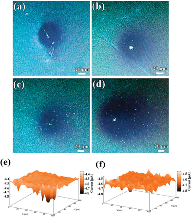 |
| | Fig. 6 Optical micrographs of the WO3 in the surrounding of [Ru(NH3)6]2+/[Ru(NH3)6]3+ redox mediator for 2 and 15 min: (a and b) compact WO3 film, (c and d) porous WO3 film. Electrochemical mappings of (e) compact WO3 film, (f) porous WO3 film. | |
4. Conclusions
The present work demonstrates the best transmittance modulation is exhibited by porous WO3 film which was successfully fabricated on different substrates by a facile, scalable and economical pulsed electrochemical deposited method with 1.1 s interval time between each pulse. The porous WO3 exhibits highly enhanced ion insertion and electrochromic properties with near theoretical optical modulation, fast switching speed, high coloration efficiency, and excellent cycling stability. Compared with the compact WO3, the porous WO3 exhibits outstanding electrochromic performance mainly due to its porous structure, which not only makes the charge-transfer and the electrolyte penetration become easier within the film, but also alleviates the expansion of the WO3 during H+ insertion and extraction. In addition, the relationships between structural and electrochemical activity of the electrochromic material were further systematically studied by SECM. These results testify that the porous structure can promote the infiltration of electrolyte and reduce the diffusion path, and consequently speed up the electrochemical activity.
Acknowledgements
This research is supported by A*Star-MND Green Building Joint Grant 1321760013. Part of the work is also supported by NTU-HUJ-BGU Nanomaterials for Energy and Water Management Programme under the Campus for Research Excellence and Technological Enterprise (CREATE) and the National Research Foundation Competitive Research Programme, Award No. NRF-CRP-13-2014-02, that is supported by the National Research Foundation, Prime Minister's Office, Singapore.
Notes and references
- P. Simon and Y. Gogotsi, Nat. Mater., 2008, 7, 845–854 CrossRef CAS PubMed.
- V. Engelhardt, S. Kuhri, J. Fleischhauer, M. Garcia-Iglesias, D. Gonzalez-Rodriguez, G. Bottari, T. Torres, D. M. Guldi and R. Faust, Chem. Sci., 2013, 4, 3888–3893 RSC.
- X. H. Yang, G. Zhu, S. H. Wang, R. Zhang, L. Lin, W. Z. Wu and Z. L. Wang, Energy Environ. Sci., 2012, 5, 9462–9466 CAS.
- C. G. Granqvist, Sol. Energy Mater. Sol. Cells, 2012, 99, 1–13 CrossRef CAS.
- M. Gratzel, Nature, 2001, 409, 575–576 CrossRef CAS PubMed.
- C. G. Granqvist, Thin Solid Films, 2014, 564, 1–38 CrossRef CAS.
- G. F. Cai, X. Wang, M. Q. Cui, P. Darmawan, J. X. Wang, A. L.-S. Eh and P. S. Lee, Nano Energy, 2015, 12, 258–267 CrossRef CAS.
- C. Park, S. Seo, H. Shin, B. D. Sarwade, J. Na and E. Kim, Chem. Sci., 2015, 6, 596–602 RSC.
- K. Wang, H. P. Wu, Y. N. Meng, Y. J. Zhang and Z. X. Wei, Energy Environ. Sci., 2012, 5, 8384–8389 CAS.
- G. A. Niklasson and C. G. Granqvist, J. Mater. Chem., 2007, 17, 127–156 RSC.
- C. G. Granqvist, Sol. Energy Mater. Sol. Cells, 2000, 60, 201–262 CrossRef CAS.
- P. H. Yang, P. Sun, Z. S. Chai, L. H. Huang, X. Cai, S. Z. Tan, J. H. Song and W. J. Mai, Angew. Chem., Int. Ed., 2014, 53, 11935–11939 CrossRef CAS PubMed.
- S. Cong, Y. Y. Tian, Q. W. Li, Z. G. Zhao and F. X. Geng, Adv. Mater., 2014, 26, 4260–4267 CrossRef CAS PubMed.
- L. Liu, M. Layani, S. Yellinek, A. Kamyshny, H. Ling, P. S. Lee, S. Magdassi and D. Mandler, J. Mater. Chem. A, 2014, 2, 16224–16229 CAS.
- R.-T. Wen, C. G. Granqvist and G. A. Niklasson, Nat. Mater., 2015, 14, 996–1001 CrossRef CAS PubMed.
- Z. H. Jiao, X. Wang, J. M. Wang, L. Ke, H. V. Demir, T. W. Koh and X. W. Sun, Chem. Commun., 2012, 48, 365–367 RSC.
- F. Lin, J. Cheng, C. Engtrakul, A. C. Dillon, D. Nordlund, R. G. Moore, T.-C. Weng, S. K. R. Williams and R. M. Richards, J. Mater. Chem., 2012, 22, 16817–16823 RSC.
- J. Thangala, S. Vaddiraju, R. Bogale, R. Thurman, T. Powers, B. Deb and M. K. Sunkara, Small, 2007, 3, 890–896 CrossRef CAS PubMed.
- N. Naseri, R. Azimirad, O. Akhavan and A. Z. Moshfegh, Thin Solid Films, 2010, 518, 2250–2257 CrossRef CAS.
- J. Zhang, X. L. Wang, X. H. Xia, C. D. Gu, Z. J. Zhao and J. P. Tu, Electrochim. Acta, 2010, 55, 6953–6958 CrossRef CAS.
- J. Zhang, J. P. Tu, X. H. Xia, X. L. Wang and C. D. Gu, J. Mater. Chem., 2011, 21, 5492–5498 RSC.
- G. F. Cai, J. P. Tu, D. Zhou, X. L. Wang and C. D. Gu, Sol. Energy Mater. Sol. Cells, 2014, 124, 103–110 CrossRef CAS.
- J. Z. Ou, S. Balendhran, M. R. Field, D. G. McCulloch, A. S. Zoolfakar, R. A. Rani, S. Zhuiykov, A. P. O'Mullane and K. Kalantar-zadeh, Nanoscale, 2012, 4, 5980–5988 RSC.
- Z. B. Cai, L. Li, J. Ren, L. B. Qiu, H. J. Lin and H. S. Peng, J. Mater. Chem. A, 2013, 1, 258–261 CAS.
- C. Y. Yan and P. S. Lee, Small, 2014, 10, 3443–3460 CrossRef CAS PubMed.
- C. Y. Yan, W. B. Kang, J. X. Wang, M. Q. Cui, X. Wang, C. Y. Foo, K. J. Chee and P. S. Lee, ACS Nano, 2014, 8, 316–322 CrossRef CAS PubMed.
- T. Pauporté, J. Electrochem. Soc., 2002, 149, C539–C545 CrossRef.
- Z. R. Yu, X. D. Jia, J. H. Du and J. Y. Zhang, Sol. Energy Mater. Sol. Cells, 2000, 64, 55–63 CrossRef CAS.
- S. H. Baeck, T. Jaramillo, G. D. Stucky and E. W. McFarland, Nano Lett., 2002, 2, 831–834 CrossRef CAS.
- I. Turyan, B. Orel, R. Reisfeld and D. Mandler, Phys. Chem. Chem. Phys., 2003, 5, 3212–3219 RSC.
- I. Turyan, U. O. Krasovec, B. Orel, T. Saraidorov, R. Reisfeld and D. Mandler, Adv. Mater., 2000, 12, 330–333 CrossRef CAS.
- S. V. Kalinin and N. Balke, Adv. Mater., 2010, 22, E193–E209 CrossRef CAS PubMed.
- M. Arca, M. V. Mirkin and A. J. Bard, J. Phys. Chem., 1995, 99, 5040–5050 CrossRef CAS.
- A. Sumboja, U. M. Tefashe, G. Wittstock and P. S. Lee, J. Power Sources, 2012, 207, 205–211 CrossRef CAS.
- A. Sumboja, U. M. Tefashe, G. Wittstock and P. S. Lee, Adv. Mater. Interfaces, 2015, 2, 1400154 Search PubMed.
- R. Cornut and C. Lefrou, J. Electroanal. Chem., 2008, 621, 178–184 CrossRef CAS.
- Y. Kazusuke, O. Hiroshi, K. Hirokazu and K. Tetsuichi, Jpn. J. Appl. Phys., 1986, 25, 1420–1426 CrossRef.
- C.-X. Qi, Z. Tan, Z.-H. Feng and L.-P. Yu, J. Mater. Sci.: Mater. Electron., 2014, 25, 1553–1558 CrossRef CAS.
- V. A. Gritsenko, Y. O. Roisin, L. E. Semenchuk and N. L. Schwarz, Solid State Commun., 1981, 38, 351–352 CrossRef CAS.
- S. H. Park, H. S. Shin, Y. H. Kim, H. M. Park and J. Y. Song, Nanoscale, 2013, 5, 1864–1869 RSC.
- Y. Sawada, A. Dougherty and J. Gollub, Phys. Rev. Lett., 1986, 56, 1260–1263 CrossRef CAS PubMed.
- D. Chatzikyriakou, N. Krins, B. Gilbert, P. Colson, J. Dewalque, J. Denayer, R. Cloots and C. Henrist, Electrochim. Acta, 2014, 137, 75–82 CrossRef CAS.
- Y. Djaoued, S. Priya and S. Balaji, J. Non-Cryst. Solids, 2008, 354, 673–679 CrossRef CAS.
- M. F. Daniel, B. Desbat, J. C. Lassegues, B. Gerand and M. Figlarz, J. Solid State Chem., 1987, 67, 235–247 CrossRef CAS.
- W. Chun-Kai, D. R. Sahu, W. Sheng-Chang, L. Chung-Kwei and H. Jow-Lay, J. Phys. D: Appl. Phys., 2012, 45, 225303 CrossRef.
- G. F. Cai, D. Zhou, Q. Q. Xiong, J. H. Zhang, X. L. Wang, C. D. Gu and J. P. Tu, Sol. Energy Mater. Sol. Cells, 2013, 117, 231–238 CrossRef CAS.
- J. Zhang, J. P. Tu, G. F. Cai, G. H. Du, X. L. Wang and P. C. Liu, Electrochim. Acta, 2013, 99, 1–8 CrossRef CAS.
- L. L. Yang, D. T. Ge, J. P. Zhao, Y. B. Ding, X. P. Kong and Y. Li, Sol. Energy Mater. Sol. Cells, 2012, 100, 251–257 CrossRef CAS.
- H.-C. Lin, C.-Y. Su, Y.-H. Yu and C.-K. Lin, J. Nanopart. Res., 2012, 14, 1–10 Search PubMed.
- G. F. Cai, X. L. Wang, D. Zhou, J. H. Zhang, Q. Q. Xiong, C. D. Gu and J. P. Tu, RSC Adv., 2013, 3, 6896–6905 RSC.
- S. H. Lee, R. Deshpande, P. A. Parilla, K. M. Jones, B. To, A. H. Mahan and A. C. Dillon, Adv. Mater., 2006, 18, 763–766 CrossRef CAS.
- A. Llordes, G. Garcia, J. Gazquez and D. J. Milliron, Nature, 2013, 500, 323–326 CrossRef CAS PubMed.
- M. Rezrazi, O. Bohnke and J. Pagetti, Displays, 1987, 8, 119–126 CrossRef CAS.
- J. Denayer, P. Aubry, G. Bister, G. Spronck, P. Colson, B. Vertruyen, V. Lardot, F. Cambier, C. Henrist and R. Cloots, Sol. Energy Mater. Sol. Cells, 2014, 130, 623–628 CrossRef CAS.
- M. Layani, P. Darmawan, W. L. Foo, L. Liu, A. Kamyshny, D. Mandler, S. Magdassi and P. S. Lee, Nanoscale, 2014, 6, 4572–4576 RSC.
- G. F. Cai, J. P. Tu, D. Zhou, L. Li, J. H. Zhang, X. L. Wang and C. D. Gu, CrystEngComm, 2014, 16, 6866–6872 RSC.
- S. Vankova, S. Zanarini, J. Amici, F. Camara, R. Arletti, S. Bodoardo and N. Penazzi, Nanoscale, 2015, 7, 7174–7177 RSC.
- J. M. Wang, E. Khoo, P. S. Lee and J. Ma, J. Phys. Chem. C, 2008, 112, 14306–14312 CAS.
- H. Z. Li, J. M. Wang, G. Y. Shi, H. Z. Wang, Q. H. Zhang and Y. G. Li, RSC Adv., 2015, 5, 196–201 RSC.
- L. C. Chen and K. C. Ho, Electrochim. Acta, 2001, 46, 2151–2158 CrossRef CAS.
- C. P. Fu, C. Y. Foo and P. S. Lee, Electrochim. Acta, 2014, 117, 139–144 CrossRef CAS.
- R. Giannuzzi, M. Balandeh, A. Mezzetti, L. Meda, P. Pattathil, G. Gigli, F. di Fonzo and M. Manca, Adv. Opt. Mater., 2015 DOI:10.1002/adom.201500152.
- C. Y. Ng, K. Abdul Razak and Z. Lockman, Electrochim. Acta, 2015, 178, 673–681 CrossRef CAS.
- J. M. Wang, E. Khoo, P. S. Lee and J. Ma, J. Phys. Chem. C, 2009, 113, 9655–9658 CAS.
- W. Xiao, W. T. Liu, X. H. Mao, H. Zhu and D. H. Wang, J. Mater. Chem. A, 2013, 1, 1261–1269 CAS.
- J.-W. Liu, J. Zheng, J.-L. Wang, J. Xu, H.-H. Li and S.-H. Yu, Nano Lett., 2013, 13, 3589–3593 CrossRef PubMed.
- H. Z. Li, G. Y. Shi, H. Z. Wang, Q. H. Zhang and Y. G. Li, J. Mater. Chem. A, 2014, 2, 11305–11310 CAS.
- W.-T. Wu, W.-P. Liao, J.-S. Chen and J.-J. Wu, ChemPhysChem, 2010, 11, 3306–3312 CrossRef CAS PubMed.
- M. Q. Cui, W. S. Ng, X. Wang, P. Darmawan and P. S. Lee, Adv. Funct. Mater., 2015, 25, 401–408 CrossRef CAS.
- W. B. Kang, C. Y. Yan, X. Wang, C. Y. Foo, A. W. Ming Tan, K. J. Zhi Chee and P. S. Lee, J. Mater. Chem. C, 2014, 2, 4727–4732 RSC.
- T. Brezesinski, D. Fattakhova Rohlfing, S. Sallard, M. Antonietti and B. M. Smarsly, Small, 2006, 2, 1203–1211 CrossRef CAS PubMed.
- J. A. Lee, M. K. Shin, S. H. Kim, H. U. Cho, G. M. Spinks, G. G. Wallace, M. D. Lima, X. Lepró, M. E. Kozlov, R. H. Baughman and S. J. Kim, Nat. Commun., 2013, 4, 1970 Search PubMed.
- X. Wang, W. S. Liu, X. Lu and P. S. Lee, J. Mater. Chem., 2012, 22, 23114–23119 RSC.
- L. B. Liu, Y. Yu, C. Yan, K. Li and Z. J. Zheng, Nat. Commun., 2015, 6, 7260 CrossRef CAS PubMed.
- Y. M. He, W. J. Chen, X. D. Li, Z. X. Zhang, J. C. Fu, C. H. Zhao and E. Q. Xie, ACS Nano, 2013, 7, 174–182 CrossRef CAS PubMed.
Footnote |
| † Electronic supplementary information (ESI) available. See DOI: 10.1039/c5sc03727a |
|
| This journal is © The Royal Society of Chemistry 2016 |
Click here to see how this site uses Cookies. View our privacy policy here. 
 Open Access Article
 This Open Access Article is licensed under a Creative Commons Attribution-Non Commercial 3.0 Unported Licence