
 Open Access Article
 This Open Access Article is licensed under a
 Creative Commons Attribution 3.0 Unported Licence
A novel design for porphyrin based D–s–A systems as molecular rectifiers†
Kavita
Garg
*a,
Chiranjib
Majumder
b,
Shiv K.
Gupta
c,
Dinesh Kumar
Aswal
c,
Sandip Kumar
Nayak
a and
Subrata
Chattopadhyay
a
aBio-Organic Division, Bhabha Atomic Research Centre, Mumbai, India. E-mail: kavitachemistry1@gmail.com; schatt@barc.gov
bChemistry Division, Bhabha Atomic Research Centre, Mumbai, India
cTechnical Physics Division, Bhabha Atomic Research Centre, Mumbai, India
First published on 16th November 2015
Abstract
Two Si-based hybrid self-assembled monolayers of porphyrin based on a D–s–A system were synthesized by electro-grafting. The monolayers showed a stable and reversible rectification at room temperature. The monolayer fabricated using a porphyrin with an eleven-carbon alkyl chain linker was comparatively more compact and exhibited a 105 times higher rectification ratio (RR) relative to another similar system that had a six-carbon alkyl chain linker, possibly because of the compact packing.
Introduction
Miniaturization is a vital need of the electronics industry, but it is limited by changes in the bulk properties of materials as they move to nanoscale dimensions. Most of the successes in this field have focused on the electrical properties of organic molecules placed between metal electrodes.1–5 In particular, self-assembled monolayers (SAMs) of alkanes and aromatic thiols on gold substrates have been very popular for constructing metal–molecule–metal (MMM) junctions.6–10 Concurrently, efforts aimed at synthesizing metal–molecule–semiconductor (MMS) junctions by covalent linking of organic molecules to semiconductor surfaces are gaining momentum.11 Such assemblies present opportunities for novel molecular electronic charge transport mechanisms, and are potentially compatible with conventional metal oxide–semiconductor (MOS) technology. To this end, there is a burgeoning interest in small organic molecules capable of switching their redox status, which, in association with semi-conductors such as Si, may scale down the size of the molecular electronic devices.12–14 Here, surface potential tailoring can be achieved by chemically-grafting organic molecules onto Si to develop improved hybrid molecular devices. For example, the p–n junction threshold voltage for rectification can be adjusted by changing the electronic nature of the organic π group molecules, instead of via the classical doping method.14 Different techniques such as making Langmuir–Blodgett (LB) films15 or SAMs of organic molecules on solid substrates via MMM junctions16 are most commonly used for this purpose. Compared to the LB films, SAMs are easy to prepare and may be more robust as the organic molecules are sturdily anchored onto the metal substrates at fixed distances. Chemically bonded monolayers on Si surfaces can be prepared either on Si oxide (SiOx) surfaces or on oxide-free Si,11,17 the latter being preferred due to better electronic coupling of the Si molecules and the lack of charging effect. In-depth reviews with excellent analyses of the different methods of fabrication and characterization of SAM junctions on H-terminated Si surfaces are available.18,19 The protocols usually adopted for constructing densely packed Si–organic hybrids involve the deposition of functionalized alkenes/alkynes using heat,20 light,21,22 electrochemical techniques, radical initiators23 or Lewis acids,24 as well as alkylhalides via either a Grignard route or lithiation.25 This is followed by attachment of the electro-active organic molecules to the terminal functionality of the resultant alkane/alkene–Si hybrids by esterification or amidation. However, due to steric factors, not all of the deposited alkane/alkene moieties can be modified with organic molecules. This may produce non-uniform organic–Si hybrids. In our previous work, we found that cathodic electro-grafting of pre-synthesized alkenylated electro-active organic molecules onto a Si–H surface can conveniently provide SAM-based molecular electronics devices with the following advantages:26 the process is simple; it can be monitored in situ to ensure completion of deposition; it can exclude oxidation and/or hydrolysis at the Si surface due to the negative potential bias of the Si wafers; and it can produce materials where the Si–H surface is modified only by the chosen molecules.Amongst the many electron-rich organic molecules, porphyrins27 are ideally suited for fabricating molecular devices because they: (i) can form stable π-cation radicals and exhibit two accessible cationic states in their monomeric forms;28–32 (ii) have long charge retention times, resulting in lower power consumption; (iii) are highly stable,33 and (iv) can form self-assembled structures.34 In view of these favourable attributes, porphyrins have been extensively used as π molecules for the construction of storage devices, molecular wires and memory devices. Reports on current rectification using C60–porphyrin combinations also exist.35 Molecules exhibiting rectification behavior with a high rectification ratio (RR) are very useful for making diodes. According to Aviram and Ratner, a single molecule with a donor–spacer–acceptor (D–s–A) structure should behave as a rectifying diode when placed between two electrodes, where the σ-bond bridge prevents the direct overlap of the donor (D) and acceptor (A) energy levels to allow unidirectional flow of current.1 Several groups have experimentally verified this model, but porphyrins have never been used for this purpose in silicon hybrid systems.36,37 In the present investigation, two such single molecules (5a/5b) were synthesized, where porphyrin and aniline moieties served as the (A) and (D) units respectively, while a –CH2–NH– moiety was anticipated to be a suitable spacer. These molecules were electro-grafted onto Si-surfaces using the C-6/C-11 alkenyl chain of 5a/5b as the linker to construct the respective MMS heterostructures. Measurement of their I–V behavior revealed high current RRs for these assemblies. Moreover, a subtle change in the linker length significantly changed the monolayer packing on the Si-surface, resulting in a pronounced alteration in the current rectification properties.
Results and discussion
Synthesis of the porphyrins
Porphyrin-based functional molecules are, by and large, synthesized via functionalization of the aryl moieties of unsymmetrical meso-tetraryl porphyrins. However, the synthesis of unsymmetrical porphyrins is fraught with limitations such as poor yields and tedious isolation procedures. Instead, functionalization of the pyrrole units of the porphyrins offers a better alternative to alter the porphyrin scaffold. However, this strategy is rarely used because the porphyrin pyrrole units are inert towards most electrophilic reactions such as Friedel–Crafts alkylation and acylation, while halogenation38 and nitration38,39 often lead to di- or higher substituted products. An exception to this is the Vilsmeier–Haack reaction, which can provide mono-formyl porphyrins in appreciable yields.39 We reasoned that the resulting formyl group could subsequently be used to construct the desired D–s–A structure for the present studies. So, following Bonfantini's method,39 tetraphenylporphyrin (TPP, 1) was converted to Cu(II)–TPP and then subjected to the Vilsmeier–Haack reaction to obtain β-formyl-TPP (2). For the synthesis of the donor part of the molecule, p-nitrophenol was o-alkylated with either 1-bromohexene or 1-bromo-10-undecene to furnish compounds 3a and 3b, respectively. These were converted to aniline derivatives 4a and 4b by reduction with Zn/HCO2NH4. Next, aldehyde 2 was separately subjected to a reductive amination using 4a or 4b to obtain the target porphyrins 5a and 5b, respectively. Previously, Welch et al.40 synthesized the Schiff's base of 2 in toluene after 72 hr, using a Dean–Stark apparatus for simultaneous removal of water. We performed the reductive amination in THF in the presence of 4 Å molecular sieves followed by a one-pot reduction of the intermediate imine to obtain 5a and 5b in improved yields (∼78%) in only 6 h (Scheme 1).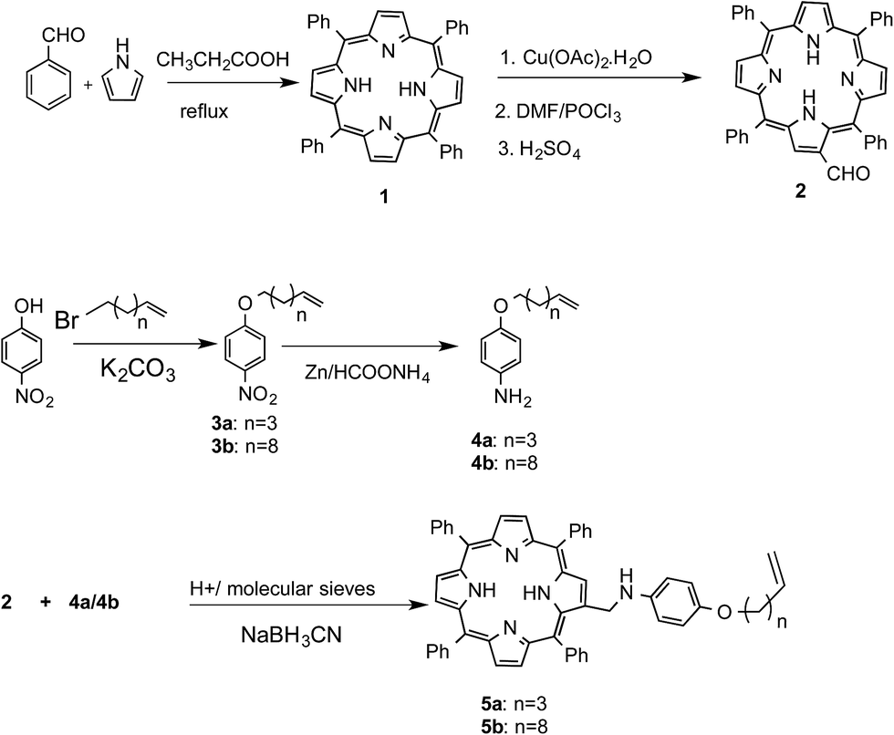 | ||
| Scheme 1 Synthesis of the D–s–A molecules 5a and 5b. | ||
Device fabrication
 | ||
| Fig. 1 CVs indicating electrografting of 5b molecules onto the Si (n++) wafers. The deposition was carried out using CV at a scan rate of 0.05 V s−1 under a N2 atmosphere with a Si wafer as the WE, Pt as the CE and Ag/AgCl as the RE. 0.1 M Bu4NP was used as the electrolyte and 5b (1 μM) was used in dry CH2Cl2. | ||
 | ||
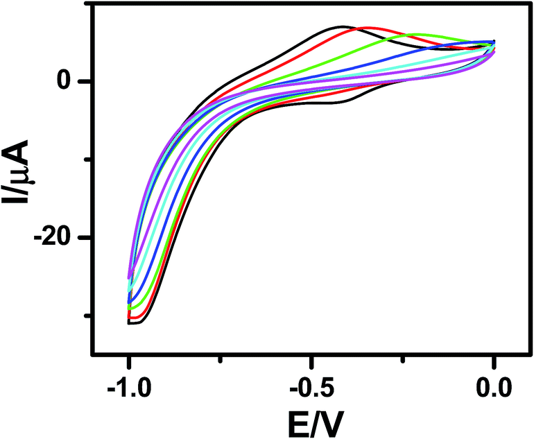
| Fig. 2 AFM images of (2 μm × 2 μm) (a) 5a and (b) 5b monolayers on Si (111). | ||
Fast scan (10 V s−1) CVs (Fig. 3) of the respective porphyrin monolayers exhibited a reversible peak at +0.8 V, confirming attachment of the porphyrin moieties. This was absent in the blank Si sample and the C-11 alkyl monolayers. The net charge transferred during the oxidation process, calculated from the area under the oxidation peak divided by the scan rate were 8.6 × 10⁻⁷ C and 2.45 × 10⁻⁶ C for 5a and 5b, respectively. Using these values, the surface coverages for the monolayers were calculated using the formula: surface coverage = total charge/(F × area dipped in electrolyte). The surface coverages were 1.11 × 10¹² and 4.5 × 10¹⁴ molecules per cm2 for 5a and 5b, respectively. Thus, the areas occupied by each molecule in the 5a and 5b monolayers were 90 nm2 and 22 Å2, respectively, indicating that 5b formed more compact monolayers than 5a. The significantly higher value for 5a compared to that previously reported19 for monolayers of simple C18-, C16-, and C12-alkanes on Si (100) revealed poor packing. This may be due to the edge-on orientation of the porphyrins.47 On the other hand, the value for the 5b monolayers matched well with the theoretically calculated diameter (14.8 Å) of TPP,48 indicating that the molecules were tightly packed due to π–π stacking, which was also revealed in the AFM images (Fig. 2). Consistent with the AFM analysis, the surface area covered by 5b was several fold that covered by 5a.
 | ||
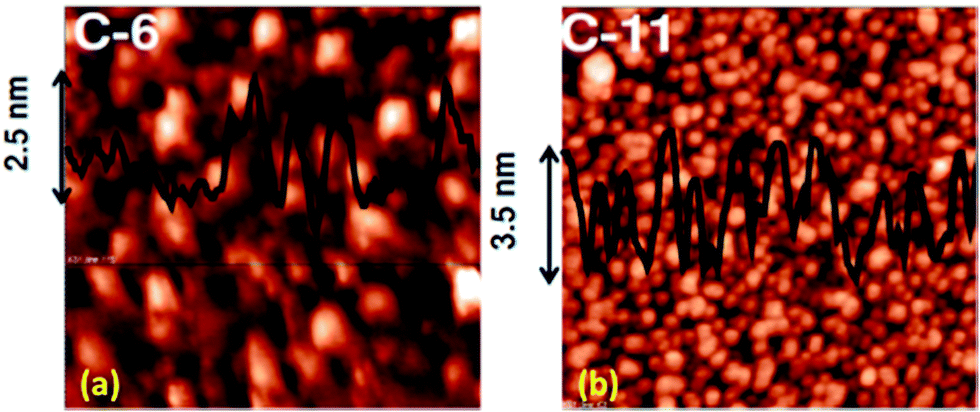
| Fig. 3 Fast scan CVs for the monolayers of (a) 5a and (b) 5b electro-grafted onto Si (n++) wafers. The CVs were recorded under a N2 atmosphere at a scan rate of 10 V s−1 using the respective monolayer-grafted Si as the WE, Pt as the CE, Ag/AgCl as the RE, and 0.1 M Bu4NP as the electrolyte. The dotted circles indicate the reversible peaks. The insets show the magnified redox peaks, after background corrections. | ||
SIMS of the 5a monolayers showed mass peaks at m/z 795, 691, 675 and 596 amu, while for the 5b monolayers peaks appeared at m/z 777 and 386 amu (Fig. 4), revealing that the molecules remained intact during the grafting process. The observed higher mass fragments, in the case of the C-11 monolayers, was consistent with its longer alkyl chain length vis-à-vis that of the C-6 monolayers.
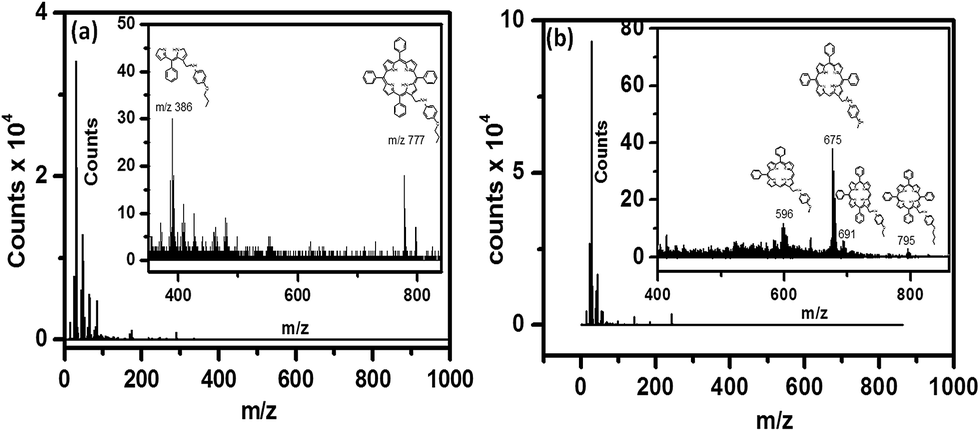 | ||
| Fig. 4 SIMS of the monolayers of (a) 5a and (b) 5b electro-grafted onto Si (n++) wafers. | ||
IR peaks due to –CH2 vibrational modes can provide better insight into the van der Waals interactions between the alkylated porphyrin rings anchored parallel on the Si surface. This, in turn, may help explain the better packing of the 5b monolayers vis-à-vis that of 5a. In pure solid alkane monolayers, the hydrocarbon chains exist in an all-trans configuration such that the carbon backbone of each molecule lies in a single plane. However, in liquid form, there is substantial out-of-plane twisting around the individual bonds, altering the frequency of the –CH2 vibrational modes.45,49 The polarized FTIR spectrum (Fig. 5) of the 5a monolayers exhibited a N–H stretching frequency at 3251 cm−1 along with symmetric (νs) and asymmetric stretching (νa) vibrational modes for the CH2 groups at 2856 and 2927 cm−1, respectively. In contrast, the respective IR absorption peaks of the 5b monolayers were at 3255, 2840 and 2921 cm−1. Our results showed that the alkyl chains in the monolayers of 5b are more rigid like those in pure solid alkanes, while those in the monolayers of 5a are twisted. This clearly explained the observed improvement in packing for the 5b (C-11 linker) monolayers over the 5a (C-6 linker) layers.50 From the X-ray photoelectron spectroscopy (XPS) data, the peak for the monolayers at 99.5 eV could be attributed to the Si–C bonds, while the absence of a SiO2 peak at 103 eV confirmed that the monolayers were free of SiO2 (Fig. SL3†).
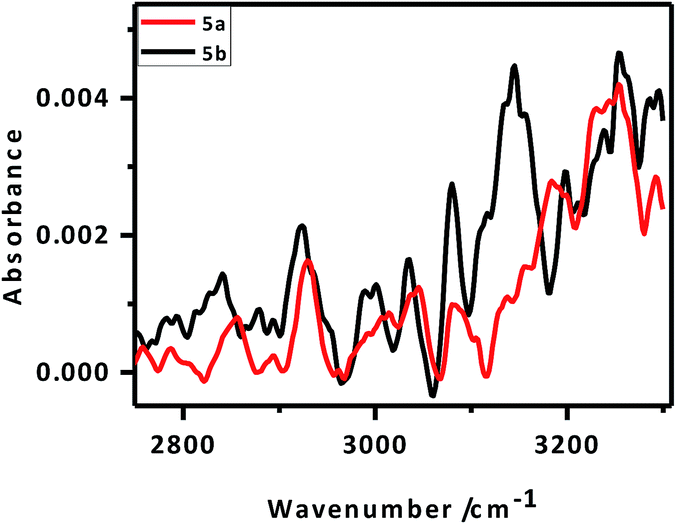 | ||
| Fig. 5 FTIR spectra of the monolayers of 5a and 5b electro-grafted onto Si (n++) wafers. | ||
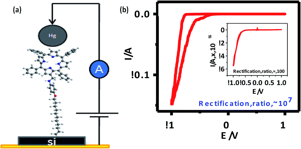 | ||
| Fig. 6 (a) I–V measurement set up; (b) experimental I–V characteristics of 5b [inset: I–V curve for 5a]. The I–V characteristics of all samples were similar, so representative curves are shown. | ||
The I–V curves (Fig. 6(b)) of the devices constructed using the monolayers of 5a and 5b showed current rectification in the reverse bias. The maximum RR was observed at ±1 V for both of the devices. The ratio for the monolayers prepared using 5b was very high (107), while that for 5a (C-6 linker) was ∼100. However, while both systems were stable during repeated voltage scanning up to 100 scans at a scan rate of 0.01V s−1, the RRs reduced gradually from their original values to ∼10![[thin space (1/6-em)]](https://www.rsc.org/images/entities/char_2009.gif) 000 for 5b and ∼10 for 5a after 50 scans.
000 for 5b and ∼10 for 5a after 50 scans.
It is already well known that when electrodes are asymmetric (and especially when the work functions of the electrode materials are different) any molecule can show current rectification.51,52 Therefore, to see the effect of using asymmetric electrodes (if any), we also recorded the I–V curves of two control devices made of (n++) Si/Hg (SL4 (a)†) and (n++) Si/C-11 alkyl monolayers/Hg (SL4 (b)†). These showed marginal rectifications with RR I+/I− values of 0.75 and 2, respectively. Recently, we constructed a n+-Si/pyrene C-11 monolayers/Hg device, which exhibited current rectification in the positive bias with RR of 100 at 1 V.53 Furthermore, a n+-Si/5-(4-undecenyloxyphenyl)-10,15,20-triphenyl porphyrin (TPP C-11) monolayers/Hg system constructed by our group showed a marginally asymmetric I–V with significant hysteresis. In the positive bias scan (0 to +0.8 V), the current jumped by an order of magnitude at +0.6 V. However, on the reverse scan (+0.8 to 0 V) the current did not retrace the curve and remained at a higher value.54 Taken together, the I–V curves of all these devices clearly indicated that the results for the present devices were not due to electrode asymmetry. Moreover, the I–V results for the n+-Si/TPP C-11 monolayers/Hg device indicated that the observed rectifications in the negative bias using the 5a/5b molecules were not due to resonance tunnelling through the TPP moiety.
The AFM and fast scan CV results showed better molecular stacking of the 5b monolayers, which may be due to the longer alkyl bridge in 5b than in 5a.55 This may contribute to the better electrical characteristics of the 5b monolayers because the overlapping of electron clouds favours the generation and transport of charge carriers to induce intrinsic conductivity. Consequently, a significantly higher maximum RR was observed for the 5b monolayers. Control experiments, carried out with a blank Si sample as well as C-11 alkyl chain-grafted Si-wafers showed nearly symmetrical sigmoidal I–V curves (Fig. SL4†), eliminating any doubt about artifacts.
The void sizes (∼0.2–0.4 nm) of the present Si–alkyl porphyrin/Hg junctions were small compared to the size of the Hg drops (∼40 μm). Therefore, Hg drops are unable to penetrate through the pinholes of the SAMs and the measured I–V is expected to be direct. Statistical analyses of the data and junction yields are extremely valuable to discriminate artifacts from the real data. Previously, Kim et al.,56 and Nijhuis et al.,57,58 employed extensive statistical analyses to assess the performance of SAM-based devices. In the present work, we constructed only 80 devices for each of compounds 5a and 5b. Nevertheless, we analyzed the statistics of our I–V results as shown in Fig. 7 and Table 1, and summarized below. For compound 5a, only 25% of the devices showed RR values of 80–100, while an additional 15% of the devices showed RR values of 50–80. However, the RR values of 44% of the devices were <50, while 16% of the devices didn't show any rectification. The device statistics for the monolayers of compound 5b were very impressive. The RR values for the majority (35%) of the devices were 105–106, while 21% of the devices showed RR values of 106–107. Another 20% showed RR values of 104–105, and the rest had RR values of 1–104. The performance of the devices made of compounds 5a and 5b were satisfactory. In particular, the RR values of the Hg/5b/Si (n++) devices were far superior to that of molecular rectifiers reported so far.53,57,58
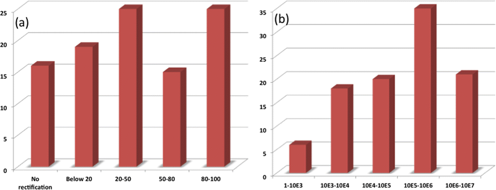 | ||
| Fig. 7 Statistics for the RR values for the devices made with (a) 5a and (b) 5b. | ||
| Molecule | No. of samples | No. of devices in each sample | Total no. of devices | No. of devices exhibiting rectification |
|---|---|---|---|---|
| 5a | 10 | 8 | 80 | 67 |
| 5b | 10 | 8 | 80 | 80 |
The current rectification properties of various D–s–A-based SAMs and LB films in contact with noble metal electrodes have been described.59 Results for some representative examples clearly establishes the significantly superior performance of the devices described in the present study. For example, a LB film of a pyrenyl carbamate in a M–M–M junction exhibited a RR value of 130 at ∼2.5 V.60 Likewise, quinolinium and tetrahydroisoquinolinium iodide-based SAMs deposited on Au substrates showed RR values of 50–150 and 30–80, respectively, at ±1 V.61,62 Meanwhile, the RR value for SAMs of quinolinium salts joined by a truncated S–C3H6 group on a Au surface was found to be 12 at ±1 V.63 In another study, a LB monolayer of the D+–π–A− molecule, hexadecylquinolinium tricyanoquinodimethanide on Au electrodes showed a maximum RR of 27.5 at 2.2 V.64
However, literature reports on metal–porphyrin–semiconductor junctions are scarce. SAMs of 4-aminothiophenol/ZnTPP/fulleropyrrolidine (PyC2C60) on a Au (111) surface showed a modest RR of 24 at 1.8 V.35 Interestingly, self-assembled layers of Fe(III)-5,15-di[4-(s-acetylthio)phenyl]-10,20-diphenyl porphyrin on annealed Au crystal facets on glass substrates showed asymmetric I–V curves with the highest RR up to 9000, but the majority of the devices showed RR = 20–200 at ±1 V.65
To confirm our current rectification results, we computed the theoretical I–V curve of the device made of 5b. Initially, the ground state (GS) geometry of molecule 5b was optimized using an ab initio molecular orbital theory based LCAO-MO approach as implemented in the GAMESS software. The ionic optimization of molecule 5b was carried out without any symmetry constraint at the B3LYP/6-31G(d,p) level of theory. To calculate the transport characteristics, a suitable device was constructed using the optimized configuration of the molecule as the central device region between two electrodes. Besides the active parts of the device, the central region also included a sufficient part of the contacts, such that the properties of the electrode regions could be described as bulk materials. This could be ensured by extending the central region into a few layers of the metallic contacts. The calculation of the electron-transport properties of the system was divided into two parts: (i) a self-consistent calculation for the electrodes with periodic boundary conditions in the transport direction, and (ii) a self-consistent open boundary calculation of the properties of the central region, where the electrodes define the boundary conditions. The complete details of the method are described in the literature.66
In the present experimental set-up, we have used a highly doped Si substrate that is expected to undergo reconstruction. This restricted accurate modelling of the molecule–substrate interface using the ab initio formalisms of our computational resources. Therefore, a model for a two-probe system was constructed (Fig. 8(a)) by placing the molecules between two Au electrodes. We modelled the electrodes as part of truncated solid crystals. Unlike Hg, which is liquid under the experimental conditions and has a complicated structure, Au possesses a well-defined face-centred cubic crystal structure. Additionally, the pseudo-potential for Au is robust and it has been tested and used by many groups as a model electrode.67,68 Understandably, the chosen system is not ideal for verification of the experimental results. However, our calculations were primarily aimed at a qualitative understanding of the electron transport through these molecules, and not a quantitative comparison, justifying our choice of Au electrodes. It is worth noting that Zheng et al.69 recently reported the NDR properties of C60 based electronic devices, wherein they claimed that the findings were independent of the type of electrodes used. For construction of the theoretical device, a thiol end group was used for attachment of the molecule with the electrode. The interface geometry of the thiol-terminated molecule and the electrode was optimized to ensure good overlap between the device and the electrodes.
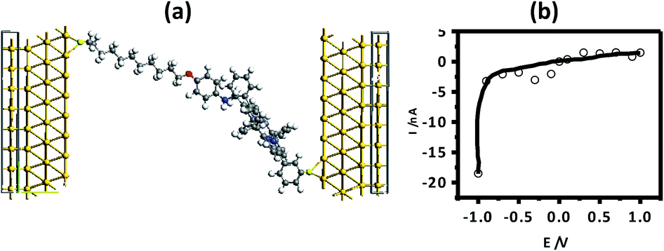 | ||
| Fig. 8 (a) Theoretical device geometry for Au/molecule 5b/Au. (b) Theoretical I–V curve. | ||
Previously, we have reported the interaction of methyl thiol, a prototype device molecule, with an extended Au(111) surface using a plane wave based pseudopotential method.70 The results showed that the terminal S atom binds at the hollow site of the Au(111) surface and the distance between the Au and S atoms is 2.52 Å. Using this information, we constructed the model for our present calculations. Two Au(111)-8X8 surfaces were used as the left and right electrodes. The Au/molecule/Au configuration was divided into three parts: left electrode, right electrode, and the central scattering region. In our models, there were three Au layers in each of the left and right electrode unit cells. The scattering region was composed of the isolated molecule together with the respective two Au layers on the left and right sides. The electron-transport properties of the Au/molecule/Au systems were investigated using the ATK 11.2.3 program, where semi-empirical extended Hückel theory, in combination with a first-principle NEGF, was employed.71 A k-point sampling of 100 was used in the electron-transport direction (Z direction).70 Consistent with the experimental results, the theoretical I–V curve also showed rectification in the reverse bias (Fig. 8(b)).
In general, the forward bias current-flow should be determined by the HOMO states of the molecules, while their respective LUMO states would dictate the reverse bias current. The observed rectification in the reverse bias is a result of an alignment of the LUMO levels of the molecules with the Fermi-levels of the electrodes. To verify this, we determined the HOMO and LUMO energy levels (Table 2) of 5b by theoretical calculations using an ab initio method (GAMESS software). Ionic optimization without any symmetry constraints was carried out at the B3LYP/6-31G(d,p) level of theory where the exchange correlation functions are expressed using hybrid density functional theory. It was observed that the HOMO of the molecule was at −4.707 eV and the LUMO at −2.062 eV. The HOMO of the molecule (located at p-aminophenol group) is in close proximity to the Fermi level of electrode, but due to non contact with the electrode, resonance tunnelling will be difficult. For the LUMO, the energy difference with the electrode Fermi level is too large to undergo resonance tunnelling. Therefore, the observed current rectification is unlikely to be due to resonant tunnelling, but molecular asymmetry (D–s–A), which favours Aviram and Ratner's mechanism for rectification.
| Energy values in eV | |||
|---|---|---|---|
| Tetraphenylporphyrin | p-Aminophenol | 5b | |
| HOMO−2 | −6.53074 | −7.97294 | −5.4757 |
| HOMO−1 | −5.52391 | −7.04775 | −5.1448 |
| HOMO | −5.30622 | −5.41507 | −4.7990 |
| LUMO | −2.55787 | −0.48981 | −2.1984 |
| LUMO+1 | −2.53066 | −0.05442 | −2.1739 |
| LUMO+2 | −0.9524 | 0 | −0.5831 |
From the spatial distribution of the HOMO and LUMO energy levels (Fig. 9), it could be seen that the HOMO was localized on the p-aminophenol segment, while the LUMO was on the porphyrin ring, and their separation by the spacer, CH2, allowed a unidirectional flow of electrons. This is consistent with the Aviram and Ratner theory that suggests that a single molecule with a donor–spacer–acceptor (D–s–A) structure should behave as a diode when placed between two electrodes if a non-conjugated σ-bond bridge prevents direct overlap of the donor and acceptor energy levels. Moreover, a monolayer will rectify if its molecules are aligned in register between two electrodes such that they work together when electrons flow from the electrode MD (attached to the acceptor) to D, and then exit from A to the electrode MA (attached to the donor).
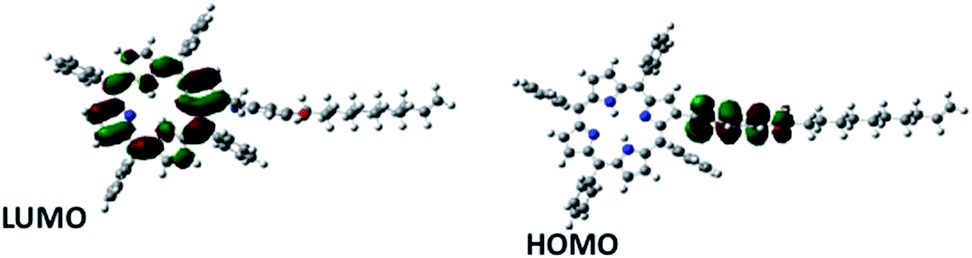 | ||
| Fig. 9 Spatial distribution of the HOMO and LUMO energy levels of 5b. | ||
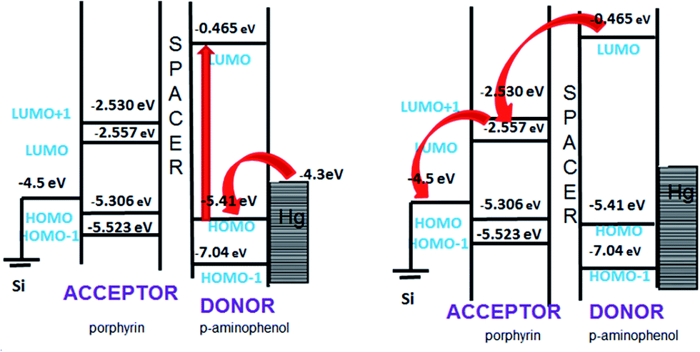
To underscore the mechanism of electron flow between the donor and acceptor moieties, we also calculated the energy levels of the individual components (p-aminophenol and TPP) of 5b using the same computational approach. The energy level diagram of the constituent species is shown in Fig. 10. The LUMO energy level of p-aminophenol was at a higher energy than the TPP moiety. This will make it the donor. Therefore, under reverse bias, when electrons flow from MD to D, the electrons will move from the HOMO of p-aminophenol to its LUMO, tunnel through the bridge to the vacant LUMO of TPP, and finally transfer to the Hg electrode to complete the reverse-direction flow.
 | ||
| Fig. 10 Mechanism of rectification for the devices made with 5b. | ||
In principle, reversing the orientation of the molecular dipole would change the I–V curves of the devices. This would also confirm that the observed rectification is not simply because of the non-symmetric nature of the device system.72 However, construction of this type of device is synthetically more demanding for the following reasons. The synthesis has to start with an unsymmetrical porphyrin, wherein the porphyrin needs to have the alkenyl attachment at one of its pyrrole moieties for grafting to the Si wafers. Synthesis of the required porphyrin proceeds via mono-bromination of the porphyrin followed by a Stille coupling with 11-trimethylstannyl undecene. Next, the unsymmetrical porphyrin needs to be formylated for the subsequent attachment of the aniline moiety. However, formylation of unsymmetrical porphyrins is never clean, and we experienced the formation of a mixture of products, formylated at different sites, and their purification was extremely cumbersome. Moreover, the grafting of such a molecule may not self-assemble in a similar manner to that used in the present work. Thus, the I–V results of the newly constructed device may provide unreliable results, despite having the reverse geometry. To confirm this hypothesis, the GS geometry of a 5b-congener having the alkenyl attachment at one of the pyrrole moieties in the porphyrin core was theoretically optimized, as done for 5b. The GS geometry of the congener revealed that both the porphyrin and aniline moieties lie on same side (Fig. SL5†). Therefore, the Si-grafted 5b-congener would be positioned in such a manner that the Hg electrode would preferably interact with the porphyrin core. However, 5b has many possible conformers, and the possibility of touching the mercury electrode by one of its straight conformers cannot be excluded. Nevertheless, based on the I–V results of the TPP C-11 monolayers54 and that of 5a/5b, it is tempting to propose that the observed current rectification is because of the nature of the molecules.
Experimental section
General
Synthesis
POCl3 (7.9 mL, 52 mmol) was added drop wise to anhydrous DMF (5.5 mL, 75.6 mmol) at 0 °C to obtain the Vilsmeier complex as a thick golden liquid. To this was added a cold suspension of the Cu(II)–porphyrinato salt (0.500 g, 0.73 mmol) in dichloroethane (50 mL). The reaction mixture was brought to room temperature, refluxed for 5 h, cooled to room temperature, and left overnight. Concentrated H2SO4 (10 mL) was added to the ice-cold mixture and stirring continued for 10 min. The green mixture was poured into ice-cold aqueous NaOH (0.625 M, 1 L) with occasional shaking until disappearance of the green colour. The mixture was extracted with CHCl3 (2 × 200 mL), then the organic layer was washed with saturated NaHCO3 (2 × 350 mL) until neutral before being dried over MgSO4. Solvent removal in vacuo followed by column chromatography (silica gel, 40% CHCl3/hexane) of the residue gave 2 (0.085 g, 75%). m.p.: >250 °C (MeOH/CHCl3); UV-Vis (CH2Cl2) λmax [nm]: 431, 526, 567, 606, 664; δH (600 MHz; CDCl3; Me4Si) 9.40 (m, 1H), 9.24 (s, 1H), 8.90 (m, 4H), 8.78 (d, J = 2.3 Hz, 2H), 8.25 (d, J = 7.0 Hz, 2H), 8.20 (m, 6H), 7.79 (m, 12H); δC (75 MHz; CDCl3; Me4Si) 189.4, 142.5, 141.9, 141.7, 135.1, 134.7, 133.5, 130.8, 129.1, 128.5, 128.2, 128.0, 127.7, 127.5, 127.1, 126.9, 122.7, 120.7, 120.4, 120.1; MALDI-TOF: m/z (%) 642 d; LCMS m/z (%): 643.3 amu. Found: C 83.84; H, 4.82; N, 8.49%. Calcd for C45H30N4O: C 84.09; H, 4.70; N, 8.72%.
3a: δH (600 MHz; CDCl3; Me4Si) 8.18 (m, 2H), 6.93 (m, 2H), 5.83 (m, 1H), 5.01 (m, 2H), 4.06 (t, J = 6.0 Hz, 2H), 2.14 (q, J = 6.0 Hz, 2H), 1.84 (quint, J = 6.8 Hz, 2H), 1.58 (m, 2H); δC (75 MHz; CDCl3; Me4Si) 164.2, 141.3, 138.3, 125.9, 115.0, 114.4, 68.7, 33.3, 28.4, 25.2; LCMS m/z (%): 222.0 amu. Found: C, 65.26; H, 6.77; N, 6.33%. Calcd for C12H15NO3: C, 65.14; H, 6.83; N, 6.33%.
3b δ H (600 MHz; CDCl3; Me4Si) 8.18 (m, 2H), 6.93 (m, 2H), 5.94 (m, 1H), 4.93 (m, 2H), 4.04 (t, J = 6.0 Hz, 2H), 2.04 (q, J = 6.0 Hz, 2H), 1.82 (quint, J = 6.6 Hz, 2H), 1.28 (m, 14H); δC (75 MHz; CDCl3; Me4Si) 164.3, 141.3, 139.2, 125.9, 114.4, 114.2, 68.9, 33.8, 29.5, 29.4, 29.3, 29.1, 29.0, 25.9; LCMS m/z (%): 292.0 amu. Found: C, 70.47; H, 8.78; N, 4.59%. Calcd for C17H25NO3: C, 70.07; H, 8.65; N, 4.81%.
5a: UV-Vis (CH2Cl2) λmax [nm]: 410, 514, 549, 589, 645; δH (300 MHz; CDCl3; Me4Si) 8.82 (m, 6H), 8.64 (d, J = 4.8 Hz, 1H), 8.17 (m, 8H), 7.73 (m, 12H), 6.72 (m, 2H), 6.48 (m, 2H), 5.83 (m, 1H), 4.98 (m, 2H), 4.45 (s, 2H), 3.88 (t, J = 6.6 Hz, 2H), 1.97–2.19 (m, 3H), 1.76 (m, 2H), 1.54 (dt, J = 15.3, 7.6 Hz, 2H), −2.79 (broad s, 2H); δC (75 MHz; CDCl3; Me4Si) 151.7, 142.4, 142.3, 142.1, 141.9, 138.7, 134.7, 134.6, 133.2, 128.5, 127.8, 127.7, 127.3, 126.8, 126.7, 120.7, 120.3, 119.5, 119.4, 115.7, 114.7, 68.6, 45.1, 33.6, 29.8, 29.0, 25.4; MALDI-TOF: m/z (%): 818. Found: C, 83.04; H, 6.08; N, 8.04%. Calcd for C57H47N5O: C, 83.69; H, 5.79; N, 8.56%.
5b: m.p.: >250 °C; UV-Vis (CH2Cl2) λmax [nm]: 411, 514, 548, 589, 646; δH (600 MHz; CDCl3; Me4Si) 8.70 (m, 6H), 8.64 (d, J = 5.9 Hz, 1H), 8.22 (m, 4H), 8.12 (m, 4H), 7.73 (m, 12H), 6.70 (m, 2H), 6.48 (d, J = 8.2 Hz, 2H), 5.81 (dd, J = 17.0, 10.0 Hz, 1H), 5.01 (d, J = 16.4 Hz, 1H), 4.95 (d, J = 10.6 Hz, 1H), 4.45 (broad s, 2H), 3.87 (t, J = 7.0 Hz, 2H), 3.74 (broad s, 1H), 2.11 (m, 2H), 1.74 (m, 2H), 1.54 (t, J = 8.2 Hz, 2H), 1.20–1.31 (m, 10H), −2.77 (broad s, 2H); δC (75 MHz; CDCl3; Me4Si) 151.8, 142.3, 142.2, 142.1, 141.9, 139.3, 134.7, 134.6, 133.2, 128.5, 127.8, 127.7, 127.3, 126.8, 126.7, 117.4, 115.7, 115.6, 114.7, 114.2, 68.8, 68.7, 33.9, 32.0, 29.8, 29.7, 29.6, 29.5, 29.2, 29.0, 26.1, 22.8, 22.2; MALDI-TOF m/z (%): 888. Found: C, 83.40; H, 6.17; N, 8.63%. Calcd for C62H57N5O: C, 83.84; H, 6.47; N, 8.56%.
:1 (v/v) mixture of conc. H2SO4:30% H2O2 (piranha solution) for 10 min at 80 °C. The wafers were washed with excess H2O and immersed successively in deaerated (purged with Ar for 30 min) 40% aqueous NH4F for 10 min and 2% aqueous HF for 2 min. The wafers were washed with deionized H2O for 1 min, dried under a stream of N2 and immediately taken into the electrochemical cell for electro-grafting.
Conclusions
Overall, we have synthesized two porphyrin-based D–s–A prototype systems (5a and 5b) with two alkenylated anilines, differing in the chain length of the alkenyl using C-6 and C-11, respectively. These were individually electro-grafted on H-terminated Si surfaces to form monolayers. The I–V characteristics of the monolayers revealed pronounced, stable and reversible current rectification at room temperature in the negative bias. To the best of our knowledge, such high RR values are rare, except for previous devices constructed by C. A. Nijhuis and Whitesides's group,51,57,58 L. Venkataraman52 and a recent publication from our own group.53 The monolayer with the C-11 linker was more compact and showed a 105 times high rectification ratio (RR) relative to the other similar system having the C-6 linker, possibly because of the compact packing. The rectification mechanism was explained on the basis of Aviram and Ratner’s theory of rectification by using ab initio molecular orbital calculations.Notes and references
- A. Aviram and M. Ratner, Chem. Phys. Lett., 1974, 29, 277–283 CrossRef CAS
.
- M. A. Reed, Science, 1997, 278, 252–254 CrossRef CAS
- R. F. Service, Science, 2001, 294, 2442–2443 CrossRef CAS PubMed
- Z. J. Donhauser, B. A. Mantooth, K. F. Kelly, L. A. Bumm, J. D. Monnell, J. J. Stapleton, D. W. Price Jr, A. M. Rawlett, D. L. Allara, J. M. Tour and P. S. Weiss, Science, 2001, 292, 2303–2307 CrossRef CAS PubMed
- M. Brink, Nature, 2002, 417, 725–729 CrossRef PubMed
- R. M. Metzger, J. W. Baldwin, W. J. Shumate, I. R. Peterson, P. Mani, G. J. Mankey, T. Morris, G. Szulczewski, S. Bosi, M. Prato, A. Comito and Y. Rubin, J. Phys. Chem. B, 2003, 107, 1021–1027 CrossRef CAS
- A. Honciuc, A. Jaiswal, A. Gong, K. Ashworth, C. W. Spangler, I. R. Peterson, L. R. Dalton and R. M. Metzger, J. Phys. Chem. B, 2005, 109, 857–871 CrossRef CAS PubMed
- R. M. Metzger, B. Chen, U. Höpfner, M. V. Lakshmikantham, D. Vuillaume, T. Kawai, X. Wu, H. Tachibana, T. V. Hughes, H. Sakurai, J. W. Baldwin, C. Hosch, M. P. Cava, L. Brehmer and G. J. Ashwell, J. Am. Chem. Soc., 1997, 119, 10455–10466 CrossRef CAS
- T. Xu, I. R. Peterson, M. V. Lakshmikantham and R. M. Metzger, Angew. Chem., Int. Ed., 2001, 40, 1749–1752 CrossRef CAS
- J. W. Baldwin, R. R. Amaresh, I. R. Peterson, W. J. Shumate, M. P. Cava, M. A. Amiri, R. Hamilton, G. J. Ashwell and R. M. Metzger, J. Phys. Chem. B, 2002, 106, 12158–12164 CrossRef CAS
- J. M. Buriak, Chem. Rev., 2002, 102, 1271–1308 CrossRef CAS PubMed
- W. Davis, W. Svec, M. Ratner and M. Wasielewski, Nature, 1998, 396, 554–63 CrossRef
- R. M. Metzger, Acc. Chem. Res., 1999, 32, 950–957 CrossRef CAS
- C. Joachim, J. K. Gimzewski and A. Aviram, Nature, 2000, 408, 541–548 CrossRef CAS PubMed
- G. J. Ashwell and D. S. Gandolfo, J. Mater. Chem., 2001, 11, 246–248 RSC
- F. Schreiber, Prog. Surf. Sci., 2000, 65, 151–256 CrossRef CAS
- S. Ciampi, J. B. Harper and J. J. Gooding, Chem. Soc. Rev., 2010, 39, 2158–2183 RSC
- H. Haick and D. Cahen, Acc. Chem. Res., 2008, 41, 359–366 CrossRef CAS PubMed
- A. Vilan, O. Yaffe, A. Biller, A. Salomon, A. Kahn and D. Cahen, Adv. Mater., 2010, 22, 140–159 CrossRef CAS PubMed
- A. B. Sieval, A. L. Demirel, J. W. M. Nissink, M. R. Linford, J. H. van Der Maas, W. H. D. Jeu, H. Zuilhof and E. J. R. Sudhölter, Langmuir, 1998, 14, 1759–1768 CrossRef CAS
- J. Terry, M. R. Linford, C. Wigren, R. Cao, P. Pianetta and C. E. D. Chidsey, Appl. Phys. Lett., 1997, 71, 1056 CrossRef CAS
- M. P. Stewart and J. M. Buriak, Angew. Chem., Int. Ed., 1998, 37, 3257–3260 CrossRef CAS
- M. R. Linford, P. Fenter, P. M. Eisenberger and C. E. D. Chidsey, J. Am. Chem. Soc., 1995, 117, 3145–3155 CrossRef CAS
- J. Buriak and M. Allen, J. Am. Chem. Soc., 1998, 120, 1339–1340 CrossRef CAS
- A. Bansal, X. Li, I. Lauermann and N. S. Lewis, J. Am. Chem. Soc., 1996, 118, 7225–7226 CrossRef CAS
- D. K. Aswal, S. P. Koiry, B. Jousselme, S. K. Gupta, S. Palacin and J. V. Yakhmi, Phys. E., 2009, 41, 325–344 CrossRef CAS
- M. Jurow, A. E. Schuckman, J. D. Batteas and C. M. Drain, Coord. Chem. Rev., 2010, 254, 2297–2310 CrossRef CAS PubMed
- L. Esaki, Phys. Rev., 1958, 109, 603–604 CrossRef CAS
- H. Lawrence and G. Ralph, Annu. Rev. Phys. Chem., 1992, 43, 437–463 CrossRef
- K. M. Roth, N. Dontha, R. B. Dabke, D. T. Gryko, C. Clausen, J. S. Lindsey, D. F. Bocian and W. G. Kuhr, J. Vac. Sci. Technol., B, 2000, 18, 2359–2364 CAS
- D. Gryko, J. Li, J. R. Diers, K. M. Roth, D. F. Bocian, W. G. Kuhr and J. S. Lindsey, J. Mater. Chem., 2001, 11, 1162–1180 RSC
- K. M. Roth, J. S. Lindsey, D. F. Bocian and W. G. Kuhr, Langmuir, 2002, 18, 4030–4040 CrossRef CAS
- K. M. Roth, A. A. Yasseri, Z. Liu, R. B. Dabke, V. Malinovskii, K.-H. Schweikart, L. Yu, H. Tiznado, F. Zaera, J. S. Lindsey, W. G. Kuhr and D. F. Bocian, J. Am. Chem. Soc., 2003, 125, 505–517 CrossRef CAS PubMed
- X. Lu, M. Li, C. Yang, L. Zhang, Y. Li, L. Jiang, H. Li, L. Jiang, C. Liu and W. Hu, Langmuir, 2006, 22, 3035–3039 CrossRef CAS PubMed
- F. Matino, V. Arima, M. Piacenza, F. Della Sala, G. Maruccio, R. J. Phaneuf, R. Del Sole, G. Mele, G. Vasapollo, G. Gigli, R. Cingolani and R. Rinaldi, ChemPhysChem, 2009, 10, 2633–2641 CrossRef CAS PubMed
- T. E. Mallouk and H. Lee, J. Chem. Educ., 1990, 67, 829–834 CrossRef CAS
- A. Giraudeau, H. J. Callot, J. Jordan, I. Ezhar and M. Grossz, J. Am. Chem. Soc., 1979, 101, 3857–3862 CrossRef CAS
- H. K. Hombrecher, V. M. Gherdan, S. Ohm, J. A. S. Cavaleiro, M. Da Graça, P. M. S. Neves and M. de Fátima Condesso, Tetrahedron, 1993, 49, 8569–8578 CrossRef CAS
- E. E. Bonfantini, A. K. Burrell, W. M. Campbell, M. J. Crossley, J. J. Gosper, M. M. Harding, D. L. Officer and D. C. W. Reid, J. Porphyrins Phthalocyanines, 2002, 06, 708–719 CrossRef CAS
- C. Welch, S. J. Archibald and R. W. Boyle, Synthesis, 2009, 551–556 CAS
- L. Zhang, L. Li, S. Chen and S. Jiang, Langmuir, 2002, 18, 5448–5456 CrossRef CAS
- Y. J. Liu, N. M. Navasero and H. Z. Yu, Langmuir, 2004, 20, 4039–4050 CrossRef CAS PubMed
- J. K. Bal, S. Kundu and S. Hazra, Chem. Phys. Lett., 2010, 500, 90–95 CrossRef CAS
- Y. Coffinier, G. Piret, M. R. Das and R. Boukherroub, C. R. Chim., 2013, 16, 65–72 CrossRef CAS
- M. Perring, S. Dutta, S. Arafat, M. Mitchell, P. J. A. Kenis and N. B. Bowden, Langmuir, 2005, 21, 10537–10544 CrossRef CAS PubMed
- S. Lenfant, D. Guerin, F. Tran Van, C. Chevrot, S. Palacin, J. P. Bourgoin, O. Bouloussa, F. Rondelez and D. Vuillaume, J. Phys. Chem. B, 2006, 110, 13947–13958 CrossRef CAS PubMed
- X. Qian, Z. Tai, X. Sun, S. Xiao, H. Wu and Z. Lu, Thin Solid Films, 1996, 284–285, 432–435 CrossRef CAS
- W. R. Scheidt, Acc. Chem. Res., 1977, 10, 339–345 CrossRef CAS
- R. L. Cicero, M. R. Linford and C. E. D. Chidsey, Langmuir, 2000, 16, 5688–5695 CrossRef CAS
- X. Qiu, C. Wang, Q. Zeng, B. Xu, S. Yin, H. Wang, S. Xu and C. Bai, J. Am. Chem. Soc., 2000, 122, 5550–5556 CrossRef CAS
- L. Yuan, R. Breuer, L. Jiang, M. Schmittel and C. A. Nijhuis, Nano Lett., 2015, 15, 5506–5512 CrossRef CAS PubMed
- B. Capozzi, J. Xia, O. Adak, E. J. Dell, Z. Liu, J. C. Taylor, J. B. Neaton, L. M. Campos and L. Venkataraman, Nat. Nanotechnol., 2015, 10, 522–527 CrossRef CAS PubMed
- K. Garg, C. Majumder, S. K. Nayak, D. K. Aswal, S. K. Gupta and S. Chattopadhyay, Phys. Chem. Chem. Phys., 2015, 17, 1891–1899 RSC
- S. P. Koiry, D. K. Aswal, A. K. Chauhan, V. Saxena, S. K. Nayak, S. K. Gupta and J. V. Yakhmi, Chem. Phys. Lett., 2008, 453, 68–72 CrossRef CAS
- X. Wang, P. E. Colavita, K. M. Metz, J. E. Butler and R. J. Hamers, Langmuir, 2007, 23, 11623–11630 CrossRef CAS PubMed
- T.-W. Kim, G. Wang, H. Lee and T. Lee, Nanotechnology, 2007, 18, 315204 CrossRef
- C. A. Nijhuis, W. F. Reus, J. R. Barber, M. D. Dickey and G. M. Whitesides, Nano Lett., 2010, 10, 3611–3619 CrossRef CAS PubMed
- C. A. Nijhuis, W. F. Reus and G. M. Whitesides, J. Am. Chem. Soc., 2009, 131, 17814–17827 CrossRef CAS PubMed
- G. J. Ashwell and A. Mohib, J. Am. Chem. Soc., 2005, 127, 16238–16244 CrossRef CAS PubMed
- A. C. Brady, B. Hodder, A. Scott Martin, J. Roy Sambles, C. P. Ewels, R. Jones, P. R. Briddon, A. M. Musa, C. A. Panetta and D. L. Mattern, J. Mater. Chem., 1999, 9, 2271–2275 RSC
- G. J. Ashwell and A. Mohib, J. Am. Chem. Soc., 2005, 127, 16238–16244 CrossRef CAS PubMed
- G. J. Ashwell, A. Mohib, C. J. Collins and A. Aref, Synth. Met., 2009, 159, 2282–2285 CrossRef CAS
- G. J. Ashwell, W. D. Tyrrell and A. J. Whittam, J. Mater. Chem., 2003, 13, 2855–2857 RSC
- R. M. Metzger, T. Xu and I. R. Peterson, J. Phys. Chem. B, 2001, 105, 7280–7290 CrossRef CAS
- X. Wang, G.-C. Wang and K. M. Lewis, Mater. Chem. Phys., 2012, 136, 190–195 CrossRef CAS
- S. Datta, Superlattices Microstruct., 2000, 28, 253–278 CrossRef CAS
- A. Nitzan and M. A. Ratner, Science, 2003, 300, 1384–1389 CrossRef CAS PubMed
- M. Di Ventra, S. T. Pantelides and N. D. Lang, Phys. Rev. Lett., 2000, 84, 979 CrossRef CAS PubMed
- X. Zheng, W. Lu, T. A. Abtew, V. Meunier and J. Bernholc, ACS Nano, 2010, 4, 7205–7210 CrossRef CAS PubMed
- C. Majumder, H. Mizuseki and Y. Kawazoe, J. Chem. Phys., 2003, 118, 9809–9813 CrossRef CAS
- K. Stokbro, D. E. Petersen, S. Smidstrup, A. Blom, M. Ipsen and K. Kaasbjerg, Phys. Rev. B: Condens. Matter Mater. Phys., 2010, 82, 1–7 CrossRef
- A. C. Brady, B. Hodder, A. S. Martin, J. R. Sambles, C. P. Ewels, R. Jones, P. R. Briddon, A. M. Musa, C. A. Panetta and D. L. Mattern, J. Mater. Chem., 1999, 9, 2271–2275 RSC
Footnote |
| † Electronic supplementary information (ESI) available: Schematic representation of the electro-grafting mechanism, the electrochemical deposition of undecene, I–V characteristics of the blank Si sample and C-11 alkyl monolayers on a silicon wafer, XPS of the monolayers and the optimised geometry of the 5b congener with reverse geometry. Tables of atom coordinates and absolute energies used for theoretical calculations. See DOI: 10.1039/c5sc03590b |
| This journal is © The Royal Society of Chemistry 2016 |