
A highly sensitive flexible SnS thin film photodetector in the ultraviolet to near infrared prepared by chemical bath deposition
Mohamed S.
Mahdi
*ab,
K.
Ibrahim
a,
A.
Hmood
c,
Naser M.
Ahmed
a,
Shrook A.
Azzez
ab and
Falah I.
Mustafa
b
aUniversiti Sains Malaysia, School of Physics, Penang 11800, Malaysia. E-mail: msaleh196730@gmail.com
bRenewable Energy Directorate, Ministry of Science and Technology, Baghdad, Iraq
cMicroelectronics and Nanotechnology Research Laboratory (M. N. R. Lab.), University of Basrah, College of Science, Physics Department, Basrah, Iraq
First published on 6th December 2016
Abstract
This study involves a novel fabrication of a high performance, low cost and flexible (SnS nanoflake based) photodetector on a polyethylene terephthalate (PET) substrate by using chemical bath deposition. The photoresponse properties of the fabricated SnS nanostructure in the ultraviolet (UV) to near infrared (NIR) region were studied. The photodetector was subjected to illumination from four light emitting diodes (LEDs) characterized by spectra peaks of 380, 530, 750 and 850 nm, respectively. The photodetector exhibited a good photoresponse, fast response and high reproducibility with time. The sensitivity values of the photodetector were determined to be approximately 2990, 1604, 2591, and 446 for wavelengths of 380, 530, 750, and 850 nm at a bias voltage of 3 V. At the bias voltage of 5 V, the sensitivity values of 2575, 1262, 1635 and 295 were recorded for 380, 530, 750 and 850 nm respectively. The photodetector also manifests fast photoresponse for the illumination wavelengths. Based on the abovementioned results, in addition to its low cost, flexibility, and non-toxic nature, the SnS photodetector is a promising photoelectronic device that is effectively applicable over the UV-vis-NIR range.
Introduction
Light sensing in the range of the ultraviolet-visible (UV-vis) to near infrared (NIR) region is of considerable importance for all kinds of scientific and industrial applications such as environmental monitoring, image sensing, communication, day and night surveillance, communication, remote control, chemical/biological sensing and wide spectral switches.1–5 Based on the wavelength range of operation, photodetectors are generally classified into two kinds of sub-systems: narrow band response detectors (UV, vis and infrared) and broadband response detectors.2 However, Yourong et al., (2014) stated that the majority of previous studies focused on the fabrication of a variety of nanoscale high-performance non flexible photodetectors including single-nanostructure ones that are applicable to a single band at room temperature.1 Nonetheless, flexible electronic and optoelectronic devices have garnered significant interest in the manufacture of liquid crystal displays, future paper displays, energy-storage devices and wearable devices,6–8 due to their exceptional properties that include flexibility, biocompatibility, light weight, softness, shock resistance, and transparency.6,8 Meantime, the research focus has shifted to flexible photo-detectors because of their suitability for specific applications in fields that specially require light weight, flexible, and mechanical shock-resistive sensing elements (such as portable devices, civil engineering and aerospace science).6 However, flexible photodetectors based on different materials with different morphologies are still being constrained to distinct photodetection regions such as single-crystalline ZnGa2O4 nanowires9 and ZnS–ZnO heterostructure nanofilms10 in the UV region, organolead halide perovskite,2 ZnO–CdO heterojunction nanofiber arrays,3 CdS nanowires,7 and Cu2O/ZnO hybrid nanofilms11 in UV-vis region, Sb2S3 nanoneedles and Nanoflowers12 and SnS nanoribbons13 in Vis region, and finally Bi2S3 Nanosheets14 for vis-NIR region. It is noticed that only few studies have been carried out on broadband photodetectors operating in the UV-NIR range.1 Moreover, the fabrication of flexible, nontoxic, low-cost, broad band and high performance photodetectors that can operate at room temperature remains a challenge. Furthermore, environmentally benign materials such as tin sulphide (SnS) have garnered much interest in the manufacture of photovoltaic and photodetectors devices because of their relatively lower toxicity and simpler disposal requirements as compared to heavy metals (e.g. Pb, Hg, and Cd).15 In addition, SnS semiconductor material is cheap, non-toxic and stable under ambient conditions.16 The semiconductor belongs to the IV–VI group.17,18 It is formed with Sn as the cation and S as the anion,19,20 and preferentially crystallizes into a layered orthorhombic structure.21 The lattice parameters of the orthorhombic structure comprise a = 0.4329 nm, b = 1.1193 nm and c = 0.398 nm, where the double SnS layers are perpendicular to the b-axis, and the Sn and S atoms are tightly bound within the layers by weak van der Waals bonds.22 These weak forces provide a chemically inert surface that lacks dangling bonds and surface density of states. As a result, the semiconductor's surface does not manifest Fermi level pinning that normally causes a high environmental and chemical stability.17,23,24 However, SnS has a narrow band gap energy of 1.35 eV with a high absorption coefficient ∼105 cm−1.25SnS nanostructure thin films have been fabricated by using different techniques such as RF magnetron sputtering,26 successive ion layer adsorption and reaction (SILAR),27 electron beam deposition,28 thermal evaporation,29 spray pyrolysis,30 electro-deposition,31 and chemical bath deposition (CBD).32–35 The SnS thin film has been used to fabricate optoelectronic devices by different researchers. For example, Deng et al., used ultra thin single-crystalline SnS nanoribbons to fabricate field-effect transistor (FET) on SiO2/Si substrate for the detection of blue, green and red light.36 Lu et al. fabricated SnS nanoparticles based photodetector on SiO2/Si substrate to detect the red light in different gas environments (air, vacuum, O2 and NH3).37 Wang et al., deposited large-size SnS thin crystals on SiO2/Si substrate to application of gas sensor for NO2 and photodetector for 405, 445, 532 and 632 nm.38
SnS has also been synthesized on glass substrates using chemical bath deposition.32–35 However, there is no report on the deposition of SnS nanostructures on PET substrate by using chemical bath deposition technique. Therefore, this work offers a novel approach to successfully depositing SnS nanostructure on PET substrate using the chemical bath deposition technique. Moreover, this is the first study on the fabrication of highly sensitive and fast photoresponse flexible broadband photodetector with coverage range of UV to NIR. The as-fabricated flexible photodetector are expected to manifest relatively higher Ilight/Idark ratio and faster photoresponse under all the broadband illumination compared to SnS nanoribbons.
Experimental procedure
The chemical bath deposition (CBD) technique was employed to grow nanostructure tin sulphide (SnS) thin film of orthorhombic structure. 0.1 M of stannous chloride (SnCl2·2H2O), 0.15 M of thioacetamide (C2H5NS), and 0.2 M non-toxic complexing agent tri-sodium citrate (TSC) (Na3C6H5O7) dissolved in 50 mL of deionized water were poured into the chemical bath. The whole mixture was homogeneously agitated with motorized magnetic stirrer at room temperature. To adjust pH of the solution, ammonium solution was added drop-wise with constant stirring. The pH of the bath was maintained 7. The PET substrate was ultrasonically cleaned in propanol 2 and deionized water, in that order for 10 min prior to film deposition. The deposition was carried out for 4 h at 80 °C. Afterwards, the substrates were removed from the beaker, washed with deionized water, and dried in open air. The deposited film was found to be brown in colour and uniformly dispersed over the substrate.The prepared SnS thin film nanostructures were confirmed by high resolution X-ray diffractometer (HXRD) using CuKα1 radiation in the 2θ range of 10 to 80°. The phases of the as-prepared SnS thin film nanostructures was confirmed by Raman spectra measurements using He–Ne laser as the excitation source operated at wavelength of 633 nm (20 mW) (Renishaw inVia Raman Microscope). The surface morphology of the thin film was analyzed using a field emission scanning electron microscope (FESEM) and energy dispersive X-ray analysis (EDX) (FEI Nova NanoSEM 450). The absorbance spectrum of the thin film was obtained for wavelength range of 320–1200 nm using UV-vis-NIR spectrophotometer (Cary model). The spectral responsivity of photodetector was carried out using a 200 W Hg (Xe) lamp as a light source, with a monochromator connected to a computer installed with the software V 4.01 of Cornerstone Utility Programming for wavelength selection. The output light intensity from light emitting diodes and 200 W Hg (Xe) lamp was measured with a Newport power meter (model 2936-C USA). The photoresponse measurements were performed under the illumination from four light emitting diodes with wavelength peaks of 380, 530, 750 and 850 nm using Keithley 2400 as a source meter. All the above measurements were performed at room temperature.
Results and discussion
The obtained XRD pattern of the prepared SnS thin film is shown in Fig. 1(a). The analysis shows that the film has a distinct peak at 39.68° corresponding to either the (041) orientation of SnS or (304) orientation of Sn2S3. One weak reflection peak was also observed at 35.64° corresponding to (303) orientation of the orthorhombic structures of Sn2S3 [JCPDS card number: 01-075-2183]. In addition, two weak reflection peaks were also observed at 42.90° and 44.26°, corresponding to (210) and (141) orientations, respectively of the orthorhombic structures of SnS [JCPDS card number: 00-39-0354]. The presence of additional tin sulphide phases (Sn2S3) with SnS phase is consistent with the previous reports.39–44 However, the presence of one distinct and three low intense peaks of the thin film may be attributed to the broad and high intensity peak of PET substrate.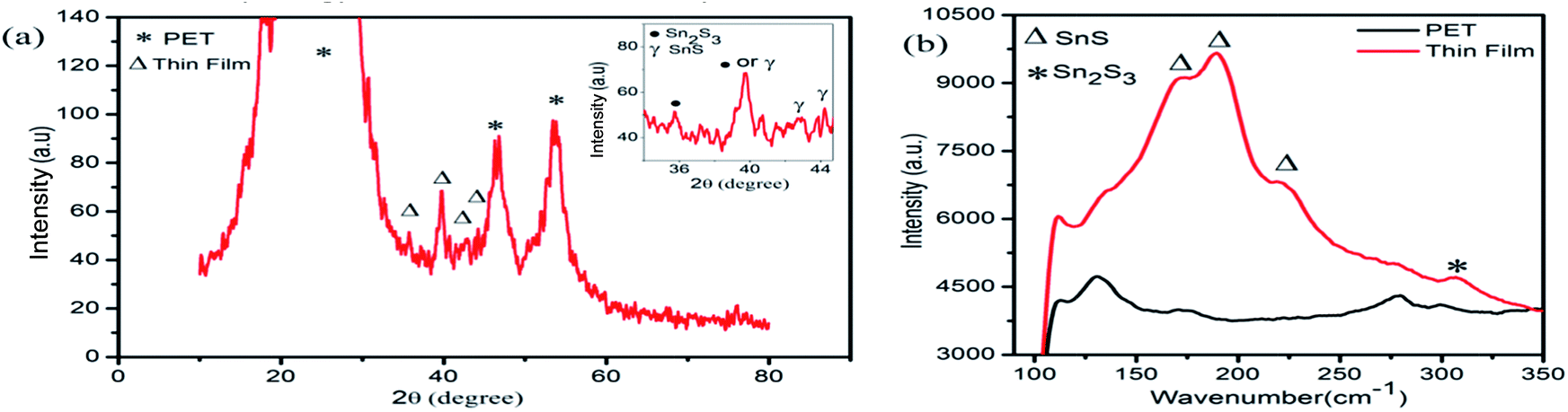 | ||
| Fig. 1 (a) X-ray diffraction pattern of the thin film (b) Raman spectra of the PET and as-synthesized nanoflakes. | ||
Due to the overlapping of SnS, SnS2 and Sn2S3 peaks in XRD diffraction pattern, the verification of the precise phases is slightly problematic.45 Therefore, Raman analysis was performed to substantiate the SnS phases46 because this analysis is more sensitive to compositional and structural changes of the material.45 In addition, Raman spectroscopy is effective for probing the crystal quality and vibration properties of the SnS nanostructures.13 In this regard, Fig. 1(b) shows Raman spectrum of the PET substrate and as-prepared SnS thin film nanostructure in the range of 100–400 cm−1. Five distinct peaks are clearly observed at 111, 171, 188, 222 and 308 cm−1. The Raman peaks at 111, 188 and 222 cm−1 are assigned to Ag mode, which are consistent with earlier reports on Raman spectra of SnS single crystal.47–50 The peaks at 171 and 308 cm−1 can be assigned to B2g mode47 and Sn2S3 phase,44,51 respectively. The combined presence of Sn2S3 with SnS has been earlier observed by Jayasree et al., when they used the same technique to prepare SnS thin film.44 From the Raman spectrum, it can be inferred that the thin film contains a major SnS phase with Sn2S3 as the minor phase.
Field emission scanning electron microscopic (FESEM) images of the deposited film were obtained with two different magnifications, as shown in Fig. 2. In low magnification, image of the thin film nanostructure depicts uniform and high-density elongated nanoflake-like grain morphology with pinholes and crack free surface. It can be observed that the substrate surface was completely covered with dense nanoflake-like, as a result increasing the number of nucleation sites.52 The high magnification image manifests that the porous-like structure was formed; consequently this structure increases the surface to volume ratio, which in turn increases light absorption.53 This increase in light absorption enhances electron–hole pairs generation, which leads to increase the resultant photocurrent and it consequently improves the performance of photodetector.
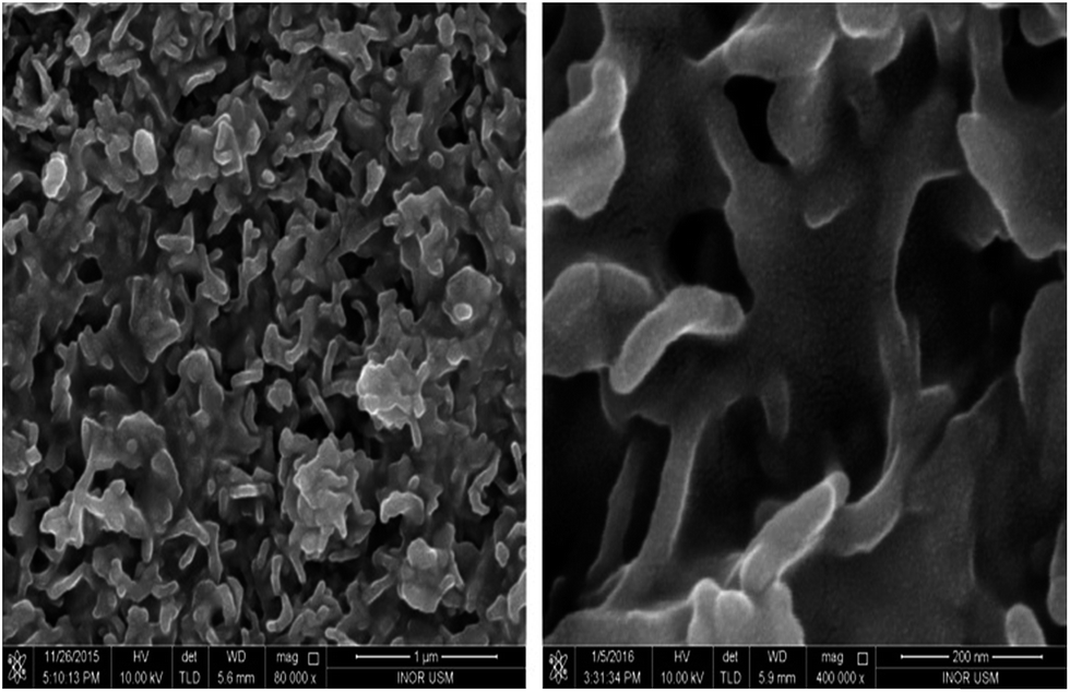 | ||
| Fig. 2 FESEM images of as-synthesized SnS nanoflakes with two different magnifications. | ||
The film thickness was calculated by a gravimetric method, and the film thickness is approximately 300 nm.
The energy band gap and type of optical transition of the SnS film deposited on PET substrate were determined using the optical absorption technique for the range of 320–1200 nm. The UV-vis-NIR absorbance spectra of the SnS nanostructure thin film which insets in Fig. 3 reveals broad and strong absorption peaks in the range of 320–800 nm. The absorption reduced with increasing wavelength. The energy band gap of the film was calculated from the absorbance spectra using the following relation.55
| αhν = B(hν − Eg)n, | (1) |
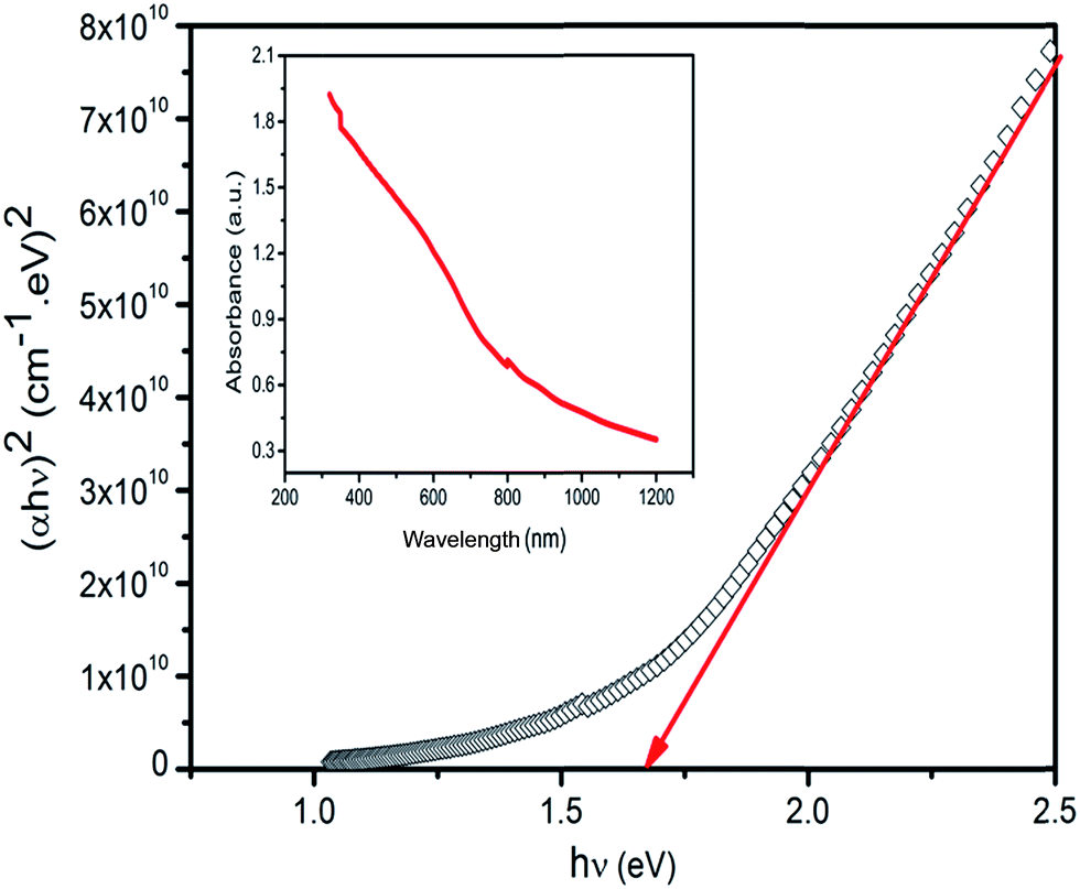 | ||
| Fig. 3 (αhν)2 against hν for SnS thin film. The inset shows the UV-vis-NIR absorbance spectra. | ||
The DC sputtering was used to deposit platinum (Pt) electrodes (100 nm thickness) on top of SnS nanoflakes at room temperature through metal mask in order to fabricate a metal–semiconductor–metal (MSM) photo-detector device, which is applicable over UV to near IR. The distance between the electrodes was 0.35 mm.
Fig. 4(a and b) presents a real image of the device and the schematics of the device for measuring the photocurrent in SnS nanoflakes. The effective area of the device was determined to be 0.187 cm2.
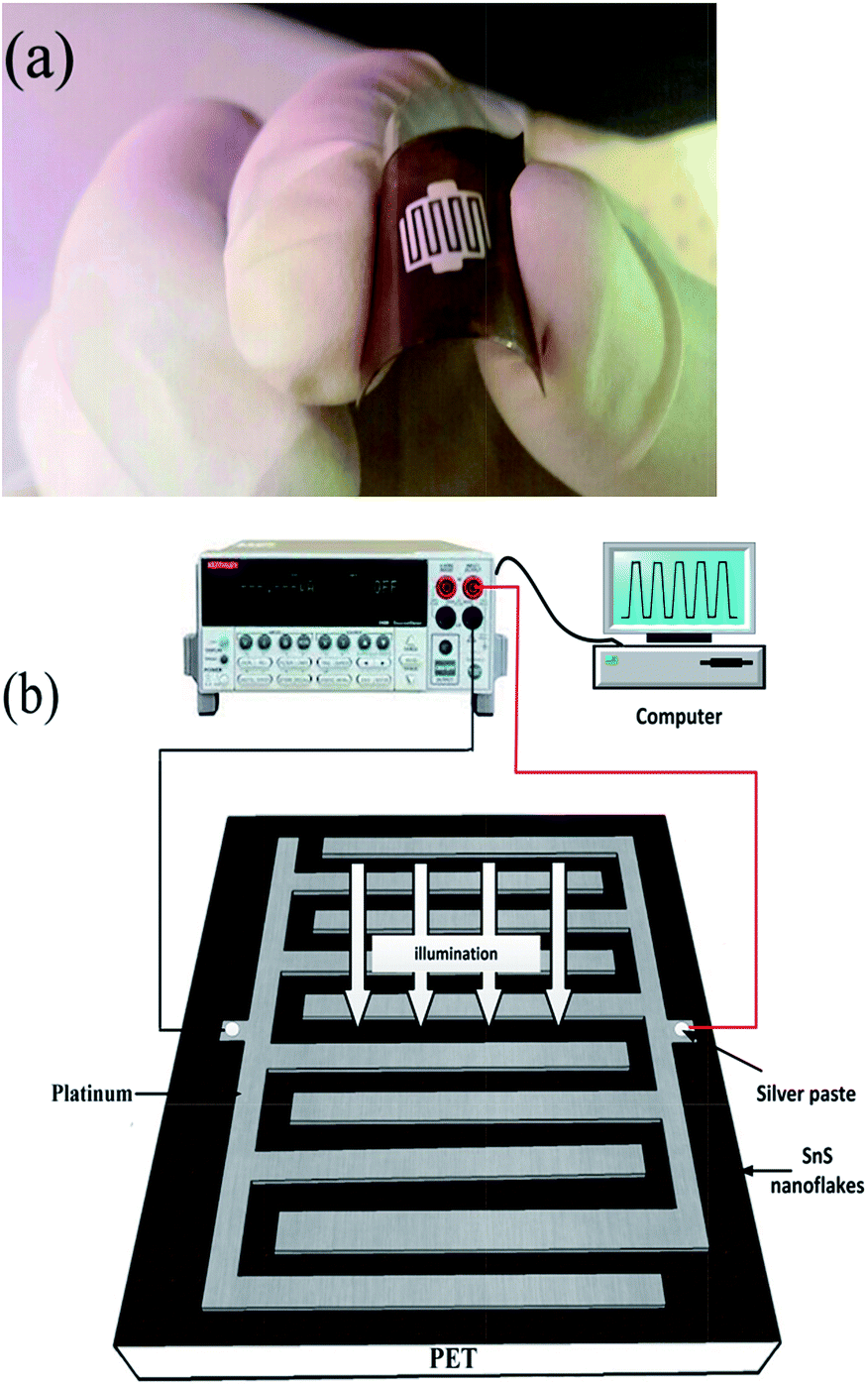 | ||
| Fig. 4 (a) Real image of the device; (b) the schematics of the device for measuring the photocurrent in SnS nanoflakes. | ||
The amount of photocurrent generated by the incident light on the effective area of a photodetector is defined as photodetector responsivity.60 The responsivity is a significant parameter that determines the sensitivity of photodetector device and is expressed as61
| Rλ = ΔIλ/(PλA) | (2) |
The dependence of the photodetector responsivity on the light wavelengths from 300 to 1000 nm at a bias voltage of 5 V is depicted in Fig. 5(a). The responsivity values are in the order of 10−6 A W−1 for the wavelength range from 300 to 800 nm, indicating a good responsivity from UV to NIR. This result is different from other materials such as ZnO,62 ZnS,63 TiO2,64 CdS65 and CuO66 that exhibit narrower band responsivity. This disparity may be attributed to the orthorhombic crystal structure of SnS. Furthermore, the photodetector results showed that the responsivity values have the same order from UV to NIR region, but different from SnS2 nanosheet results because they have different values for the different regions.1
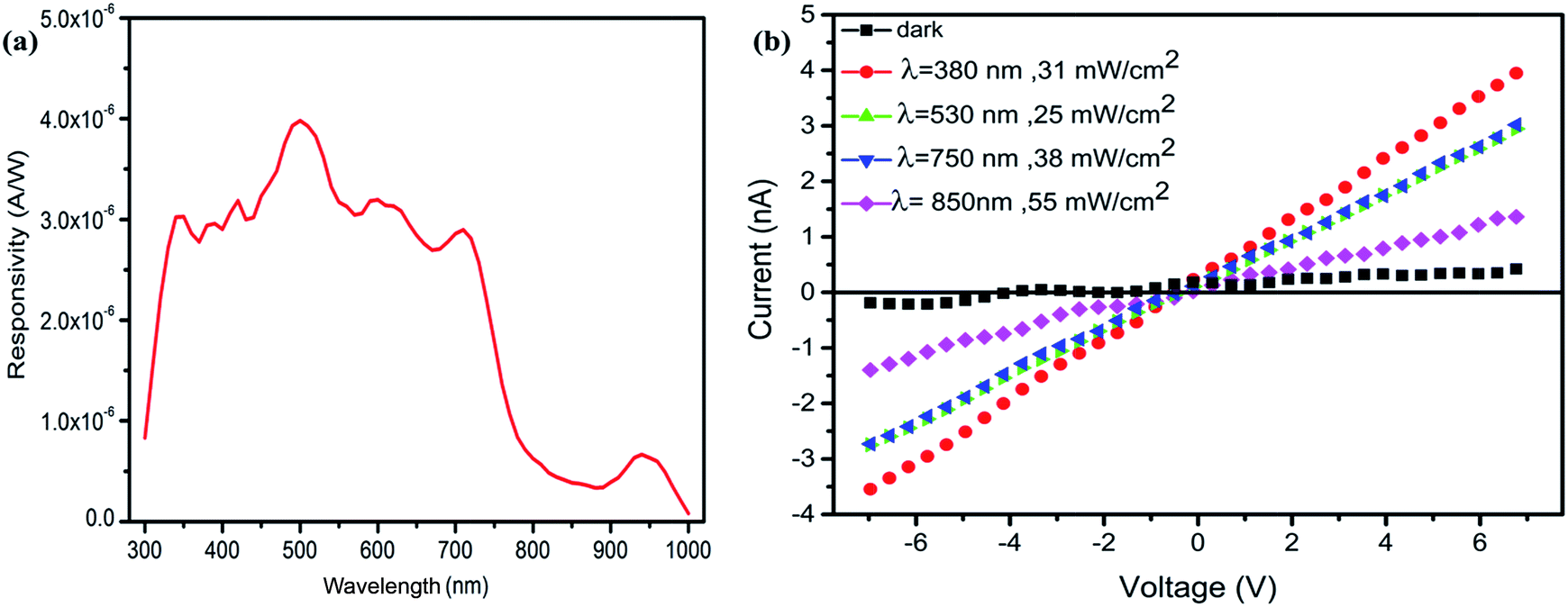 | ||
| Fig. 5 (a) The spectral responsivity of the photodetector (b) the current–voltage curves of the photodetector under dark and illumination with different wavelengths light. | ||
The current–voltage characteristics of SnS based MSM photodetector under dark and light illumination at different wavelengths conditions are shown in Fig. 5(b). The linearity and symmetry of the curves suggest a good ohmic contact between the Pt electrodes and the SnS nanostructure. This behaviour can be attributed to the lower work function of SnS P-type (4.2 eV)67 compared to the work function of Pt value (5.6 eV).68 This indicates that Pt/SnS interface strongly follows the tunnelling transport mechanism.67Fig. 5(b) shows a comparative analysis of the photocurrent measurements in relation to dark current for wavelengths from 380 to 850 nm. At the same bias voltage, the current significantly increases when the photodetector is subjected to light illumination. This is indicated by the very high photosensitivity (ratio of photocurrent to the dark current)11,69 of the device in the UV to NIR region.
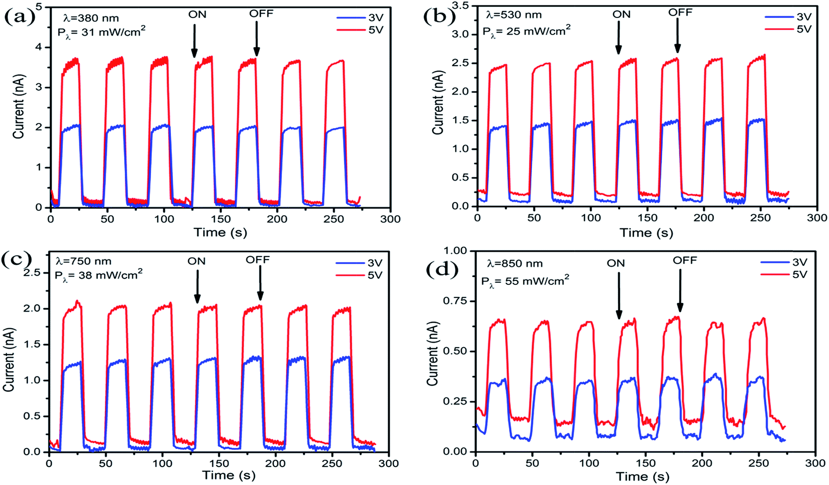
The dependence of the current on time at 3 and 5 V bias voltages under alternating dark and illumination conditions with ON/OFF switch cycle of 20 s at different wavelengths are shown in Fig. 6(a–d). This figure shows that the maximum value of the photocurrent after several cycles remains unchanged and relatively stable for all the wavelengths. This indicates that the flexible device is highly reproducible and stable. In addition, the photocurrent increased to a stable value under illumination, and then dramatically decreased to its initial value as the illumination was turned off, thereby showing excellent stability and reproducible characteristics. Furthermore, the photocurrent is dependent on the mechanism of photoconductivity, given that it originates from the electron–hole pairs generated by illumination with energy above the energy band gap of the semiconductor. Fig. 6 reveals that the excitation of tin sulphide thin film by photon energy exceeding its energy band gap significantly increases the photocurrent value higher than when compared to the value generated by energy below the energy band gap, denoting that the sub-band gap states contributes little to the photocurrent creation.12 In addition, it is obvious that the photocurrent increases with applied bias voltage due to the increase in the carrier drift velocity (v), which is directly proportional to the applied bias voltage (V) as shown in the following equation70
 | (3) |
 | (4) |
 | ||
| Fig. 6 The current–time curves of the photodetector under on/off switch illumination with different wavelengths light at 3 and 5 V bias voltages, (a) 380 nm. (b) 530 nm. (c) 750 nm. (d) 850 nm. | ||
The sensitivity (S) is one of significant parameters that determines the photodetector quality, and is given by66,72
 | (5) |
The sensitivity values of the photodetector were determined in Fig. 6(a–d) to be approximately 2990, 1604, 2591 and 446 for wavelength peaks, and of 380, 530, 750 and 850 nm, respectively, at the bias voltage of 3 V. At the bias voltage of 5 V, the sensitivity values of 2575, 1262, 1635 and 295 were recorded for 380, 530, 750 and 850 nm, respectively. The sensitivity at 530 nm is higher more ten times when compared to the sensitivity value obtained for large-size SnS thin crystals on SiO2/Si substrate (∼130 for the 532 nm at incident light intensity of 50 mW cm−2).38 Generally, comparable high photocurrent/dark-current ratios (sensitivity) are resulted from a low dark current.3 So, it can be seen that the sensitivity values at 5 V bias voltage are less when compared to 3 V for all wavelengths. This result can be attributed to the increasing in photocurrent is less than dark current with increasing bias voltage, so the sensitivity decreases with increasing bias voltage. This result is in agreement with the previous report.66 The highest sensitivity value (2290) recorded at 380 nm is attributed to the high absorbance at this wavelength as observed in Fig. 3. Conversely, the lowest sensitivity value (466) observed at 850 nm is possibly recorded as a result of insufficient energy of the incident radiation required to generate a large number of electron–hole pairs. Therefore, less numbers of photocarriers were generated causing the sensitivity to abruptly decrease. The photogenerated carriers for 850 nm are originated from the photo-responsible defects present within the band gap.73 These defects are named as persistent photoconductivity (PCC)73,74 that are originated from Sn vacancies, Sn2+, Sn4+ ionized states of Sn and S vacancies. The Sn vacancies create shallow accepter levels in band gap,75,76 while S vacancies and Sn2+, Sn4+ ionized states of Sn and create donor levels.76 This deduction is consistent with the previous studies on zinc oxides, which similarly pointed out that intrinsic defects in zinc oxide causing detection were observed under below energy band gap illumination.73
In addition, from Fig. 5(a) which relates the responsivity with wavelength, shows the responsivity value at 530 nm is higher as compared to 380 nm, while Fig. 6, that relates photocurrent with time for different wavelengths, manifests 380 nm as a maximum sensitivity. This difference can be attributed to the light intensity of 380 nm (31 mW cm−2) which is higher than what used in case of 530 nm (25 mW cm−2) in Fig. 6. Moreover, the set of two measurements are different. While, the spectral responsivity of photodetector was carried out by using a 200 W Hg (Xe) lamp as a light source. Whereas the measurements of photocurrent with time were performed by using four separated light emitting diodes. Furthermore, it is known the relation between photocurrent and light intensity obey power relation and that relation is non linear, it is a consequence of the complex processes of electron–hole generation, trapping and recombination within the semiconductor.77
Based on the previous reports, Sn2S3 semiconductor exhibits n-type conductivity.54,78,79 The presence of Sn2S3 in SnS film would act as a electron trap for majority carriers (i.e., holes) in SnS; similarly, any SnS presented in an Sn2S3 sample would act as a hole trap for majority carriers (i.e., electrons) in Sn2S3.78 Therefore, the photodetector device manifests low dark current value (low conductivity), possibly due to the presence of tin sulphide phase Sn2S3 in the film,78 and consequently generating high sensitivity in the photodetector device. Moreover, the low current value helps to enhance the signal to the noise ratio of the detector since shot noise is proportional to dark current as earlier reported by Farhat et al., (2015).80 The low dark current also indicates low detectability light intensity.71
I light/Idark ratio values were determined to be 31, 17, 27, and 5 for 380, 530, 750 and 850 nm, respectively, at the bias voltage of 3 V. At the bias voltage of 5 V, Ilight/Idark ratio values of 27, 14, 17, and 4 were recorded for 380, 530, 750, and 850 nm, respectively. These values are relatively higher when compared to the Ilight/Idark value obtained for SnS nanoribbons (22 for the visible light at incident light intensity of 300 mW cm−2).13
The rise and decay times are the time needed for the photocurrent to increase from 10% to 90% of its maximum value and decrease from 90% to 10% of its maximum value respectively.81 The rise and decay times of a single on/off cycle at 3 bias voltages were found to be about 0.52, 0.52, 0.64 and 2.96 s, while the decay times were determined to be 0.51, 0.49, 0.50 and 1.59 s for 380, 530, 750 and 850 nm, respectively, at 3 V bias voltage. At 5 V bias voltage, the rise times include 0.67, 0.53, 0.55 and 3.64 s; while the decay times comprise 0.52, 0.50, 0.53 and 1.0 s for 380, 530, 750 and 850 nm, respectively. The response time of device at 850 nm is long if compared to other wavelengths because the detection is originated from the photo-responsible defects present within the band gap. These defects lead to increase the response time.82
In addition, from the rise and decay time values, it is clearly noted that there is only a small negligible difference in these values. For example, the rise time and decay time values at 5 V bias voltage are found to be 0.53 s and 0.50 s respectively at 530 nm. These values are so close to each other that the difference is negligible. This small difference in the rise and decay time values might be due to slight instability in the pulses. The photoresponse time results (rise and decay) revealed that the very fast rise and decay times were recorded compared with earlier nanoribbons SnS flexible photodetector which showed that the rise and decay times are 5.4 and 1.8 s respectively.13
To further study the influence of various incident light intensity on the photoresponse properties of the as-grown SnS nanoflakes device, the photocurrent were measured under different given incident light intensity. Fig. 7(a) shows the photoresponse of the device illuminated with 380 nm at different incident light intensities at a bias voltage of 5 V. As expected, illumination by higher light intensities leads to more photon-flux density, resulting in more number of electron–hole pairs generated.61,83 The corresponding photocurrent–incident light intensity curve is plotted in Fig. 7(b). The relationship between the photocurrent and the incident light intensity illumination could be fitted by a power law3,84
| Iph = CPλγ | (6) |
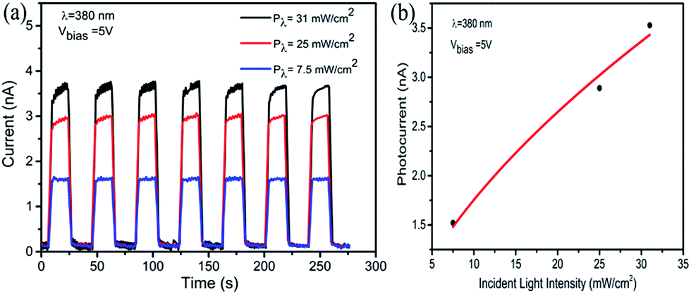 | ||
| Fig. 7 (a) Current–time curves of the device illuminated under 380 nm light at various incident light intensities. (b) The light intensity dependence of the photocurrent under the bias voltage of 5 V. | ||
The present SnS nanoflakes based photodetector established high Ilight/Idark ratio, excellent stability and fast rise and decay times. In addition, no work on UV-vis-NIR flexible photodetectors based on SnS nanostructure has been reported so far. As a result of this research, we may confirm that this work constructs a good candidate for high performance photodetector. Table 1 summarizes the rise times, decay times, Ilight/Idark ratios, and sensitivities for the different wavelengths (380, 530, 750 and 850 nm) employed in this study in addition to a comparative analysis against previous reports of SnS photodetector.
| Substrate | V | λ (nm) | P λ (mW cm−2) | Rise/decay Times (s) | I light/Idark | S (%) | Reference |
|---|---|---|---|---|---|---|---|
| SiO2/Si | 0.1 | Red light (650 nm) | — | 0.45/0.56 | — | — | 37 |
| SiO2/Si | 2 | 405 | 50 | 0.09/0.09 | — | ∼70 | 38 |
| 445 | ∼70 | ||||||
| 532 | ∼130 | ||||||
| 632 | ∼70 | ||||||
| Glass | 10 | Tungsten-halogen | 100 | — | 3.5 | — | 32 |
| PET | 10 | Xenon lamp | 300 | 5.4/1.8 | 22 | — | 13 |
| PET | 5 | 380 | 31 | 0.67/0.52 | 27 | 2990 | This work |
| 530 | 25 | 0.53/0.50 | 14 | 1262 | |||
| 750 | 38 | 0.55/0.53 | 17 | 1635 | |||
| 850 | 55 | 3.64/1.0 | 4 | 295 | |||
| PET | 3 | 380 | 31 | 0.52/0.51 | 31 | 2575 | |
| 530 | 25 | 0.52/0.49 | 17 | 1604 | |||
| 750 | 38 | 0.64/0.50 | 27 | 2591 | |||
| 850 | 55 | 2.96/1.59 | 5 | 446 |
It is known that the adsorption and desorption of oxygen molecules in the dark and upon illumination on the SnS nanoflakes surface play a key role in photo-conduction mechanism.12,77,88 The electrons are the majority carriers in n-type semiconductors, such as ZnO, CdS, TiO2, ZnS and Sn2S. The exposure of a sample to air induces oxygen adsorption on the sample surface as well as the capture of free electrons from the surface sample, which creates a low conductivity depletion layer at the sample surface.12,77,88 This depletion layer on the surface of semiconductors increases the device resistance. However, the situation is quite different in the case of p-type semiconductors. The electron affinity and energy band gap of SnS are 3.14 eV 67 and 1.65 eV, respectively. Thus, the adsorbed oxygen with chemical potential of approximately 5.7 eV,89 which is below the vacuum energy, will form acceptor levels close to the valence band at the surface, resulting in the formation of an accumulation layer for SnS with holes as majority carriers rather than electrons in the case of n-type semiconductors. Consequently, the trapped electrons leave more holes obtainable close to the surface, and thus decreasing the device resistance. Adsorption of oxygen molecules process is described by the following:
| O2(g) + e− → O2−(ads) + vacancySn+ + hole | (7) |
So the device resistance decreases by oxygen adsorption. This result was proved by Xie and his group, where they showed that the resistivity of CuO device under a vacuum is comparably higher than in air due to the surface oxygen adsorption.89
Conclusion
In summary, a novel flexible photodetector based on SnS nanoflakes was fabricated on PET substrate by simple and low cost chemical bath deposition technique. The flexible photodetector exhibits a good photoresponse from UV to NIR region. In addition, the results reveal excellent reproducibility over time, high sensitivity, and high photocurrent at the bias voltage 3 and 5 V. The results of this study may pave the way to create a new prospect for the potential applications of the SnS nanoflakes in the field of broadband response photodetectors, electronic devices, and flexible optoelectronics.Acknowledgements
The authors are grateful for the Nano-Optoelectronics Research and Technology Laboratory (N.O.R.) of the School of Physics, Universiti Sains Malaysia for the help given to perform this research.Notes and references
- Y. Tao, X. Wu, W. Wang and J. Wang, J. Mater. Chem. C, 2015, 3, 1347 RSC.
- X. Hu, X. Zhang, L. Liang, J. Bao, S. Li, W. Yang and Y. Xie, Adv. Funct. Mater., 2014, 24, 7373 CrossRef CAS.
- Z. Zheng, L. Gan, H. Li, Y. Ma, Y. Bando, D. Golberg and T. Zhai, Adv. Funct. Mater., 2015, 25, 5885 CrossRef CAS.
- J. S. Jie, W. J. Zhang, Y. Jiang, X. M. Meng, Y. Q. Li and S. T. Lee, Nano Lett., 2006, 6, 1887 CrossRef CAS PubMed.
- R. Dong, C. Bi, Q. Dong, F. Guo, Y. Yuan, Y. Fang, Z. Xiao and J. Huang, Adv. Opt. Mater., 2014, 2, 549 CrossRef CAS.
- X. Wang, W. Song, B. Liu, G. Chen, D. Chen, C. Zhou and G. Shen, Adv. Funct. Mater., 2013, 23, 1202 CrossRef CAS.
- Y. Pei, R. Pei, X. Liang, Y. Wang, L. Liu, H. Chen and J. Liang, Sci. Rep., 2016, 6, 21551 CrossRef CAS PubMed.
- G. Chen, W. Wang, C. Wang, T. Ding and Q. Yang, Adv. Sci., 2015, 2, 1500109 CrossRef PubMed.
- Z. Lou, L. Li and G. Shen, Nano Res., 2015, 8, 2162 CrossRef CAS.
- W. Tian, C. Zhang, T. Zhai, S.-L. Li, X. Wang, J. Liu, X. Jie, D. Liu, M. Liao, Y. Koide, D. Golberg and Y. Bando, Adv. Mater., 2014, 26, 3088 CrossRef CAS PubMed.
- X. Liu Hejun Du, P. Wang, T.-T. Lim and X. W. Sun, J. Mater. Chem. C, 2014, 2, 9536 RSC.
- J. Chao, B. Liang, X. Hou, Z. Liu, Z. Xie, B. Liu, W. Song, G. Chen, D. Chen and G. Shen, Opt. Express, 2013, 21, 13639 CrossRef CAS PubMed.
- J. Chao, Z. Wang, X. Xu, Q. Xiang, W. Song, G. Chen, J. Hu and D. Chen, RSC Adv., 2013, 3, 2746 RSC.
- G. Chen, Y. Yu, K. Zheng, T. Ding, W. Wang, Y. Jiang and Q. Yang, Small, 2015, 11, 2848 CrossRef CAS PubMed.
- J. Kim, Doctor of Philosophy, The Pennsylvania State University, 2013 Search PubMed.
- E. C. Greyson, J. E. Barton and T. W. Odom, Small, 2006, 2, 368 CrossRef CAS PubMed.
- N. Koteeswara Reddy, Y. B. Hahn, M. Devika, H. R. Sumana and K. R. Gunasekhar, J. Appl. Phys., 2007, 101, 093522 CrossRef.
- N. Koteeswara Reddy, ECS J. Solid State Sci. Technol., 2013, 2, 6 Search PubMed.
- E. Guneri, F. Gode, C. Ulutas, F. Kirmizigul, G. Altindemir and C. Gumus, Chalcogenide Lett., 2010, 7, 685 CAS.
- A. Akkari, C. Guasch and N. Kamoun-Turki, J. Alloys Compd., 2010, 490, 180 CrossRef CAS.
- A. R. H. F. Ettema, R. A. de Groot, C. Haas and T. S. Turner, Phys. Rev. B: Condens. Matter Mater. Phys., 1992, 46, 7363 CrossRef CAS.
- B. Ghosh, M. Das, P. Banerjee and S. Das, Appl. Surf. Sci., 2008, 254, 6436 CrossRef CAS.
- D. Avellaneda, M. T. S. Nair and P. K. Nair, J. Electrochem. Soc., 2008, 155, 517 CrossRef.
- B. Subramaniana, C. Sanjeevirajab and M. Jayachandran, Sol. Energy Mater. Sol. Cells, 2003, 79, 57 CrossRef.
- M. Devika, K. T. Ramakrishna Reddy, N. Koteeswara Reddy, K. Ramesh, R. Ganesan, K. R. Gunasekhar and E. S. R. Gopal, J. Appl. Phys., 2006, 100, 023518 CrossRef.
- K. Hartman, J. L. Johnson, M. I. Bertoni, D. Recht, M. J. Aziz, M. A. Scarpulla and T. Buonassisi, Thin Solid Films, 2011, 519, 7421 CrossRef CAS.
- B. Ghosh, M. Das, P. Banerjee and S. Das, Appl. Surf. Sci., 2008, 254, 6436 CrossRef CAS.
- A. Tanusevski and D. Poelman, Sol. Energy Mater. Sol. Cells, 2003, 80, 297 CrossRef CAS.
- R. W. Miles, O. E. Ogah, G. Zoppi and I. Forbes, Thin Solid Films, 2009, 517, 4702 CrossRef CAS.
- N. K. Reddy and K. T. R. Reddy, Thin Solid Films, 1998, 325, 4 CrossRef.
- Z. Zaimal, M. Z. Hussin, A. Kassim and A. Ghazali, J. Mater. Sci. Lett., 1997, 16, 1446 CrossRef.
- C. Gao, H. Shen and L. Sun, Appl. Surf. Sci., 2011, 257, 6750 CrossRef CAS.
- P. Pramanik, P. K. Basu and S. Biswas, Thin Solid Films, 1987, 150, 269 CrossRef CAS.
- D. Avellaneda, G. Delgado, M. T. S. Nair and P. K. Nair, Thin Solid Films, 2007, 515, 5771 CrossRef CAS.
- F. Gode, E. Guneri and O. Baglayan, Appl. Surf. Sci., 2014, 318, 227 CrossRef CAS.
- Z. Deng, D. Cao, J. He, S. Lin, S. M. Lindsay and Y. Liu, ACS Nano, 2012, 6, 6197 CrossRef CAS PubMed.
- F. Lu, J. Yang, R. Li, N. Huo, Y. Li, Z. Wei and J. Li, J. Mater. Chem. C, 2015, 3, 1397 RSC.
- J. Wang, G. Lian, Z. Xu, C. Fu, Z. Lin, L. Li, Q. Wang, D. Cui and C.-P. Wong, ACS Appl. Mater. Interfaces, 2016, 8(15), 9545 CAS.
- V. Robles, J. F. Trigo, C. Guillén and J. Herrero, J. Mater. Sci., 2013, 48, 3943 CrossRef CAS.
- R. E. Banai, J. C. Cordell, G. Lindwall, N. J. Tanen, S.-L. Shang, J. R. Nasr, Z. K. Liu, J. R. S. Brownson and M. W. Horn, J. Electron. Mater., 2016, 45, 499 CrossRef CAS.
- M. Calixto-Rodriguez, H. Martinez, A. Sanchez-Juarez, J. Campos-Alvarez and A. Tiburcio-Silver, Thin Solid Films, 2009, 517, 2497 CrossRef CAS.
- S. Polivtseva, I. Oja Acik, A. Katerski, A. Mere, V. Mikli and M. Krunks, Energy Procedia, 2014, 60, 156 CrossRef CAS.
- L. S. Price, I. P. Parkin, A. M. E. Hardy and R. J. H. Clark, Chem. Mater., 1999, 11, 1792 CrossRef CAS.
- Y. Jayasree, U. Chalapathi and V. Sundara Raja, Thin Solid Films, 2013, 537, 149 CrossRef CAS.
- M. Vasudeva Reddy, G. Sreedevi, C. Park, R. W. Miles and K. T. Ramakrishna Reddy, Curr. Appl. Phys., 2015, 15, 588 CrossRef.
- N. R. Mathews, H. B. M. Anaya, M. A. Cortes-Jacome, C. Angeles-Chavez and J. A. Toledo-Antonio, J. Electrochem. Soc., 2010, 157, 337 CrossRef.
- P. M. Nikolic, L. Miljkovic, P. Mihajlovic and P. Lavrencic, J. Phys. C: Solid State Phys., 1977, 10, L289 CrossRef CAS.
- M. G. Sousa, A. F. da Cunha and P. A. Fernandes, J. Alloys Compd., 2014, 592, 80 CrossRef CAS.
- H. R. Chandrasekhar, R. G. Humphreys, U. Zwick and M. Cardona, Phys. Rev. B: Solid State, 1977, 15, 2177 CrossRef CAS.
- L. L. Cheng, M. H. Liu, M. X. Wang, S. C. Wang, G. D. Wang, Q. Y. Zhou and Z. Q. Chen, J. Alloys Compd., 2012, 545, 122 CrossRef CAS.
- A. Supee, Y. Tanaka and M. Ichimura, Mater. Sci. Semicond. Process., 2015, 38, 290 CrossRef CAS.
- A. M. Selman, Z. Hassan, M. Husham and N. M. Ahmed, Appl. Surf. Sci., 2014, 305, 445 CrossRef CAS.
- Z. Lou, L. Li and G. Shen, Nanoscale, 2016, 8, 5219 RSC.
- M. Khadraoui, N. Benramdane, C. Mathieu, A. Bouzidi, R. Miloua, Z. Kebbab, K. Sahraoui and R. Desfeux, Solid State Commun., 2010, 150, 297 CrossRef CAS.
- A. Akkari, C. Guasch, N. Kamoun-Turki and J. Tauu, J. Alloys Compd., 2010, 490, 180 CrossRef CAS.
- A. Gómez, H. Martínez, M. Calixto-Rodríguez, D. Avellaneda, P. Guillermo Reyes and O. Flores, J. Mater. Sci. Eng. B, 2013, 3(6), 352 Search PubMed.
- E. Guneria, C. Ulutas, F. Kirmizigul, G. Altindemir, F. Gode and C. Gumus, Appl. Surf. Sci., 2010, 257, 1189 CrossRef.
- Robert W. Miles, Ogah E. Ogah, G. Zoppi and I. Forbes, Thin Solid Films, 2009, 517, 4702 CrossRef CAS.
- O. Lopez-Sanchez, D. Lembke, M. Kayci, A. Radenovic and A. Kis, Nat. Nanotechnol., 2013, 8, 497 CrossRef CAS PubMed.
- Z. Wang, M. Safdar, C. Jiang and J. He, Nano Lett., 2012, 12, 4715 CrossRef CAS PubMed.
- Q. L. Li, Y. Li, J. Gao, S. D. Wang and X. H. Sun, Appl. Phys. Lett., 2011, 99, 243105 CrossRef.
- D. I. Son, H. Y. Yang, T. W. Kim and W. I. Park, Composites, Part B, 2015, 69, 154 CrossRef CAS.
- Y. Kim, S. Jin Kim, S.-P. Cho, B. Hee Hong and D.-J. Jang, Sci. Rep., 2015, 5, 12345 CrossRef CAS PubMed.
- A. M. Selman and Z. Hassana, Mater. Res. Bull., 2016, 73, 29 CrossRef CAS.
- L. Li, P. Wu, X. Fang, T. Zhai, L. Dai, M. Liao, Y. Koide, H. Wang, Y. Bando and D. Golberg, Adv. Mater., 2010, 22, 3161 CrossRef CAS PubMed.
- K. M. Chahrour, N. M. Ahmed, M. R. Hashim, N. G. Elfadill and M. Bououdina, Sens. Actuators, A, 2016, 239, 209 CrossRef CAS.
- M. Devika, N. Koteeswara Reddy, F. Patolsky and K. R. Gunasekhar, J. Appl. Phys., 2008, 104, 124503 CrossRef.
- X. F. Wang, L. He, S. Halas, T. Pie, J. G. Lin and T. Durakiewicz, Appl. Phys. Lett., 2013, 102, 223504 CrossRef.
- A. G. Ardakani, M. Pazoki, S. M. Mahdavi, A. R. Bahrampour and N. Taghavinia, Appl. Surf. Sci., 2012, 258, 5405 CrossRef.
- J. D. Prades, R. Jimenez-Diaz, F. Hernandez-Ramirez, L. Fernandez-Romero, T. Andreu, A. Cirera, A. Romano-Rodriguez, A. Cornet, J. R. Morante, S. Barth and S. Mathur, J. Phys. Chem. C, 2008, 112, 14639 CAS.
- Y. Fang and J. Huang, Adv. Mater., 2015, 27, 2804 CrossRef CAS PubMed.
- P. Kumar, N. Saxena, S. Dewan, F. Singh and V. Gupta, RSC Adv., 2016, 6, 3642 RSC.
- K. Kuriyama, K. Matsumoto, Y. Suzuki, K. Kushida and Q. Xu, Solid State Commun., 2009, 149, 1350 CrossRef.
- F. Jiang, H. Shen and J. Jiao, ECS J. Solid State Sci. Technol., 2013, 2, P478 CrossRef CAS.
- Y. Gupta and P. Arun, Phys. Status Solidi B, 2016, 253, 509 CrossRef CAS.
- T. H. Sajeesh, K. B. Jinesh, M. Rao, C. S. Kartha and K. P. Vijayakumar, Phys. Status Solidi A, 2012, 209, 1274 CrossRef CAS.
- H. Kind, H. Q. Yan, B. Messer, M. Law and P. D. Yang, Adv. Mater., 2002, 14, 158 CrossRef CAS.
- L. A. Burton, D. Colombara, R. D. Abellon, F. C. Grozema, L. M. Peter, T. J. Savenije, G. Dennler and A. Walsh, Chem. Mater., 2013, 25, 4908 CrossRef CAS.
- T. Srinivasa Reddy and M. C. Santhosh Kumar, Ceram. Int., 2016, 42, 12262 CrossRef.
- O. F. Farhat, M. M. Halim, M. J. Abdullah, M. K. M. Ali, N. M. Ahmed and N. K. Allam, Appl. Phys. A, 2015, 119, 1197 CrossRef CAS.
- L. Li, Y. X. Zhang, X. S. Fang, T. Y. Zhai, M. Y. Liao, H. Q. Wang, G. H. Li, Y. Koide, Y. Bando and D. Golberg, Nanotechnology, 2011, 22, 165704 CrossRef CAS PubMed.
- M. A. Mahdi, J. J. Hassan, S. S. Ng, Z. Hassan and N. M. Ahmed, Phys. E, 2012, 44, 1716 CrossRef CAS.
- Z. Wang, M. Safdar, C. Jiang and J. He, Nano Lett., 2012, 12, 4715 CrossRef CAS PubMed.
- Y. Pei, R. Pei, X. Liang, Y. Wang, L. Liu, H. Chen and J. Liang, Sci. Rep., 2016, 6, 21551 CrossRef CAS PubMed.
- C. Soci, A. Zhang, B. Xiang, S. A. Dayeh, D. P. Aplin, J. Park, X. Y. Bao, Y. H. Lo and D. Wang, Nano Lett., 2007, 7, 1003 CrossRef CAS PubMed.
- W. Zhang, J. K. Huang, C. H. Chen, Y. H. Chang, Y. J. Cheng and L. J. Li, Adv. Mater., 2013, 25, 3456 CrossRef CAS PubMed.
- S. R. Tamalampudi, Y. Y. Lu, U. R. Kumar, R. Sankar, C. D. Liao, B. K. Moorthy, C. H. Cheng, F. C. Chou and Y. T. Chen, Nano Lett., 2014, 14, 2800 CrossRef CAS PubMed.
- C. Soci, A. Zhang, B. Xiang, S. A. Dayeh, D. P. R. Aplin, J. Park, X. Y. Bao, Y. H. Lo and D. Wang, Nano Lett., 2007, 7, 1003 CrossRef CAS PubMed.
- X. De-Hua, W. Fei-Fei, L. Hao, D. Min-Yong and X. Wen-Jie, Chin. Phys. B, 2013, 22, 058103 CrossRef.
| This journal is © The Royal Society of Chemistry 2016 |