Construction of a carbon fiber based layer-by-layer (LbL) assembly – a smart approach towards effective EMI shielding

Yudhajit Bhattacharjee, Viraj Bhingardive, Sourav Biswas and Suryasarathi Bose*
Department of Materials Engineering, Indian Institute of Science, Bangalore – 560012, India. E-mail: sbose@materials.iisc.ernet.in

Received 29th September 2016 , Accepted 17th November 2016

First published on 18th November 2016


Abstract

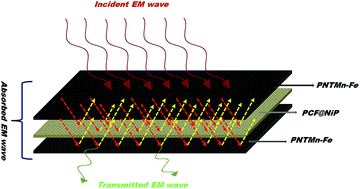
Construction of ultrathin multilayer polymer nanocomposite films by precise layer-by-layer (LbL) architectural assembly with tailor-made properties has been achieved here to block incoming EM radiation. To accomplish this, Mn (manganese)–ferrite nanoparticles were synthesized and incorporated in a thermoplastic matrix (PVDF, polyvinylidene fluoride) along with conductive MWNTs (PNTMn–Fe) by a facile solution blending process. These nanocomposite films were used as outer layers of the LbL assembly. In order to scavenge the transmitted radiation through PNTMn–Fe layers, PVDF films sandwiched with a Ni (nickel)-deposited woven carbon fiber (CF) mat (PCF@NiP), designed using a facile electroless deposition technique. These layers were used as inner layers of the LbL assembly. The different layers were then stacked and hot pressed into a composite structure. This ultrathin (0.60 mm) multilayer architecture showed an extraordinary (52 dB at 18 GHz) shielding effectiveness and thereby promises a smart approach to accomplish a lightweight, high performance, EMI shielding material.


Introduction

Enormous use of electronic devices, communication systems and other instruments are creating problems for the device itself and nearby circuitry due to electromagnetic (EM) interference among devices which degrade their performance. One of the effective ways to tackle with this problem is either shielding or arresting these EM waves.1–5 Metals are effective in this context and widely applied to block the incoming EM radiation. However, due to their associated limitations, such as expense, heaviness and susceptibility to corrosion, light-weight polymeric composites with effective electromagnetic interference (EMI) shielding performance are becoming potential substitutes in this electronic world, which is rapidly switching to miniaturization.6–11 Today, carbon derivatives like carbon fiber (CF), carbon nanotubes (single walled, multi-walled), and graphene possessing high electrical conductivity, a high aspect ratio and better mechanical properties, are claimed to be deserving candidates for fabrication of high performance composites.12–18 The interface between fibre and the matrix plays a pivotal part in composite properties.19–21 Due to their outstanding electrical conductivity and high aspect ratio, multi wall carbon nanotubes (MWNTs) are the ideal nanofillers in composites which have been extensively used to give an understanding towards research on hybrid composites.20,22–25 Recently, interest is mounting in the development of hybrid (or multi-scale or hierarchical) materials, in which nanoscale reinforcement is utilized in conjunction with traditional micro-scale carbon fibers.23,26 It is well known that carbon fibers are extensively used in applications due to their high strength, high aspect ratio and better electrical conductivity.27–29 Hence, in order take advantage of these properties woven carbon fibers (CF) mats are utilized in the present work. EM radiation consists of two vector components (electrical and magnetic) which are perpendicular to each other, so to circumvent such consequences, materials that contain both electric and magnetic dipoles are required. So, designing new hybrid nanomaterials is the burgeoning research interest. In recent past, many researchers have tried to incorporate neat carbon fibers, as well as electrodeposited carbon fibers for shielding applications.19,30,31 There are various methods available to deposit metal particles onto carbon fibers viz. electrochemical deposition, electro less deposition etc.19,30,32 However, since electroless deposition is simple, efficient, and inexpensive and does not require external sources,33–35 we adopted this technique in the present investigation. Furthermore, we have synthesized Mn–ferrite nanoparticles which show good magnetic properties – a key requisite for effective EM absorption. In this article we have designed and fabricated a layer by layer (LbL) assembly of soft nanocomposites consisting of PVDF, electroless deposited carbon fiber mat (PCF@NiP) and a thin film of PNTMn–Fe. Here, we believe that the PCF@NiP along with intercalated thin film of PNTMn–Fe, composite will work in tandem and play a vital role in attenuating EM radiation.

The one-pot synthesis of Mn–ferrite is depicted in Fig. 1a. TEM image (see Fig. 1b) corroborates the fact that the facile one pot synthesis technique that was implemented here for the synthesis of Mn–ferrite nanoparticles is fairly robust. The average particle size is in the range of ca. 20 nm as established from corresponding TEM images (Fig. 1). In order to study the surface elemental composition, a thorough investigation was carried out using EDS mapping which confirms the formation of Mn–ferrite nanoparticle 1 (d and e). Magnetic hysteresis was obtained by using room temperature VSM. Fig. 1f, depicted that saturation magnetization (MS) is 33.7 emu g−1, remnant magnetization (MR) is 8.03 emu g−1 and coercively (HC) is 27 Oe, for the designed Mn–ferrite nanoparticles. As inferred from Fig. 1g, crystalline Fe3O4 is a contaminant in the obtained spinel Mn–ferrite nanoparticles. However, this contaminant was not eliminated from the final product as this may help in enhancing the magnetic moment; one of the key requirements of shielding materials.


image file: c6ra24238c-f1.tif
Fig. 1 (a) Synthetic scheme for Mn–ferrite; (b) bright-field TEM micrograph; (c) HAADF image (d) STEM mapping of Fe; (e) STEM mapping of Mn; (f) XRD analysis Mn–ferrite nanoparticles; (g) VSM plot of synthesized Mn–ferrite nanoparticles.

From the SEM micrographs, it can be easily inferred that the deposition of nickel particles onto CF mat by electroless deposition is successfully done. Fig. 2b and c shows the SEM morphologies before and after the deposition of nickel onto CF. EDAX spectra further confirms the presence of nickel particle onto CF as shown in Fig. 2d and this EDAX quantify its presence (97.20 wt% and 90.43 atomic%). It is important to stress that decorating nickel nanoparticles on CF mat will have profound impact on microwave absorption property arising from additional absorption mechanism such as Neel relaxation and the interface created by CF and nickel nanoparticles. In addition, this might improve impedance matching than pure CF mat. It is envisaged that CF mat act as a waveguide and the microwave absorption strongly depend on the geometric array and the spacing between the fibers. The electroless deposition technique that was adopted here will ensure the integrity of the pure CF which rather is destroyed in harsh chemical functionalization processes.


image file: c6ra24238c-f2.tif
Fig. 2 (a) Schematic illustration of (PCF@NiP) (b) SEM micrograph of neat carbon fiber (c) SEM micrograph of (PCF@NiP) (d) EDAX spectra showing nickel peaks.

A smart approach was adopted here with an objective to accomplish maximum attenuation of incoming EM radiation. The outer layers of the LbL assembly were chosen specifically to absorb the incoming EM radiation through a pseudo-network of Mn–ferrite and MWNTs. The inner layers were chosen carefully so that the transmitted radiation from the outer layers can be reflected back so that the outer layers can scavenge the remaining EM radiation. Hence, these alternate layers can act in tandem to achieve maximum attenuation. The amount of attenuation of incident EM wave is analysed here by assessing the total shielding effectiveness (SET) which is expressed in dB. It reflects the quantitative measure of dissipated EM waves. Usually, when the value of SET reaches 20 dB, the material is capable of attenuating 99% of the incoming EM radiation. Here we have measured the SET of LbL assembly using a VNA coupled with a waveguide in the 12–18 GHz frequency region. It is well known from the literature that EM radiation is the harmonized proliferation of electric and magnetic vector component, which are perpendicular to each other. In this context, to circumvent such consequences both electric and magnetic dipoles are required, which can interact with the associated vector component of incident EM wave. It is important to know the contribution of each layer individually before their key role in the LbL assembly can be realized. The PNTMn–Fe nanocomposite shows a SET is ca. −18 dB while the neat PVDF was transparent to EM radiation (Fig. 3a). The presence of MWNTs not only provides inter connected conducting pathway inside the matrix (see Fig. S3), which is essential for charge transportation but also the high dielectric loss which scales up the shielding performance. Further Mn–ferrite directly interacts with the magnetic vector component of incident EM waves resulting in magnetic hysteresis loss. In general the higher value in permittivity and permeability mainly increase the shielding efficiency by absorption and can be explained using this equation;36

image file: c6ra24238c-t1.tif
where, μ = μ0μr and σ = 2π0ε′′. So it is clear that shielding by absorption is increased with the increasing values of μr and εr where μr = μ′ − jμ′′ and εr = ε′ − jε′′. The reflection loss can be calculated by using these relative complex parameters with the help of well-established line theory.37
image file: c6ra24238c-t2.tif

image file: c6ra24238c-t3.tif
where, c is the velocity of light and t is the thickness of the samples. Hence, studying the reflection loss can be a conclusive evidence to comment on overall shielding mechanism of the PNTMn–Fe composites. Here we plotted RL as a function of frequency from 12–18 GHz region, where the peak corresponds to absorption (minimum reflection) of incident EM radiation. Fig. 3b clearly depicted the shielding effectiveness of Mn–ferrite contain composites. Higher magnetic permeability is the key factor in enhancing the minimum RL over MWNT containing composites. Finally Mn–ferrite containing composite exhibited minimum RL of ca. −56 dB. We also calculated the natural resonance frequency of this particular ferrite (fm) by this equation;38
image file: c6ra24238c-t4.tif


image file: c6ra24238c-f3.tif
Fig. 3 (a) SET of various system. (b) Reflection loss of PNTMn–Fe, inset plot shows the reflection loss of PNT composites. (C) LbL assembly of polymer nanocomposites. (d) Storage modulus vs. temperature plot of LbL assembly, inset plot shows the storage modulus of neat PVDF (e) schematic representation of shielding mechanism of LbL assembly. (f) SEM micrograph of LbL assembly.

Due to the larger saturation magnetization a red shift is visualized from the calculated natural frequency which is 10.2 GHz. So clearly this observation demonstrates the improved absorption band width with resonance frequency.

We now focus on understanding the mechanism of shielding in the sandwich structure consisting of PVDF–CF–PVDF and PVDF–CF@Ni–PVDF (PCF@NiP) composite films. A significant improvement in SET is also observed in case of PCF@NiP as compared with the control PVDF–CF–PVDF. The attenuation of incident EM radiation could be attributed due to the interaction of both electric and magnetic dipoles of incident EM waves. Due to the local field discrepancy, the incident EM radiation interact with PCF@NiP where it gets attenuated by dipole interaction; part of EM waves get consumed to align the magnetic domains of nickel particles and the remaining gets either transmitted or absorbed by the CF mat due to associated high electrical conductivity of CF. It is envisaged that CF mat can act like a waveguide however, for effective screening of incoming EM radiation, we have deposited (electroless) Ni nanoparticles onto the CF mat. The interface between Ni nanoparticles and CF mat will result in interfacial polarization which can contribute towards absorbing the incoming EM radiation which otherwise will be reflected from pure CF mat.

The exceptional shielding performance of individual materials further led us to design layer-by-layer (LbL) stack of different polymer nanocomposites to optimize the shielding performance for designing thin shielding materials that can be explored for myriad opportunities. Stacked layer-by-layer architectural assembly was constructed by constructing PNTMn–Fe nanocomposite as outer layers and sandwiching PCF@NiP as inner layers (see Fig. 3f). The fundamental basis of such layer positioning stems from the individual shielding performance. The LbL assembly is constructed here by simple compression molding – an industrially viable technique to prepare sandwich structures. This particular LbL assembly resulted in an outstanding SET of ca. −52 dB for an ultra-thin shield of 0.60 mm thickness (Table S1). The EM attenuation is mainly due to presence of both electric and magnetic dipoles in the system. Besides in the multilayer structure the total EM shielding efficiency was increased due to heterogeneous dielectric polarizabilities between the two layers leading to accumulation of virtual charges at the interface. By carefully positioning different layers, various LbL assemblies have been designed and the obtained shielding performances are also measured (see Table S1). By positioning PNTMn–Fe as outer layers and PCF@NiP as inner layers the total shielding was slightly higher than when the latter layers were placed as outer layers (see Fig. S4).

It is important to investigate the mechanical behavior of this stacked LbL structure as a function of temperature and hence dynamic mechanical analysis was carried out. Fig. 3d exhibits storage modulus of LbL composite as a function of temperature and inset shows the DMA of neat PVDF sample. It is interesting to note that the stacked layer showed significantly higher storage modulus than neat PVDF film of similar thickness. These tests were done with a tension clamp and the results begin to suggest that there is no interlayer slip between the different soft nanocomposites which were hot-pressed – a rather industrially viable technique to mold composite structures. Detailed shielding of mechanism of composite layers is shown schematically in Fig. 3e. In Fig. 3f SEM micrograph confirms the assembling of the layers.

In summary, we have effectively developed an ultrathin LbL assembly consisting PCF@NiP nanocomposites (as outer layers) and PNTMn–Fe (as inner layers). This method of LbL assembly with appropriate illustrated an excellent EM attenuation. The multi-layered assembly of just 0.60 mm thickness exhibited an outstanding EMI shielding effectiveness of ca. −52 dB, illustrating the fact that this multilayer assembly can be considered as an economic alternative to lightweight EMI shielding material due to its easy fabrication procedure and industrially feasible techniques of processing.

Experimental section

Materials

Analytical grade reagents, stannous chloride (SnCl2) and palladium chloride (PdCl2) were supplied by Sigma Aldrich and used as received. NiCl2·6H2O, NiSO4·6H2O, NaH2PO2·2H2O, Na3C6H5O7·5H2O, NH4Cl, Pb(NO3) and NH4OH were obtained from SDFCL. Iron sulphate heptahydrate (FeSO4·7H2O), manganese chloride (MnSO4) and L-arginine was procured from Sigma-Aldrich. Analytical grade of ethanol, dimethylformamide, chloroform and tetrahydrofuran were procured form commercial sources. The pristine multi-walled carbon nanotube (MWNTs, NC7000, average diameter and length of 9.5 mm and 1.5 μm respectively with 90% purity) was obtained from Nanocyl, Belgium. Commercially available PVDF (Kynar 741) (MW 440 000 g mol−1) was procured from Arkema. Bidirectional carbon fiber, grade 200GSM (10 μm diameter, 0.25 mm thickness) were supplied by Hindustan Technical Fabrics Ltd.

Characterization

Transmission electron micrographs and HAADF (high angle annular dark field) images were acquired using a FEI Technai F30 instrument operated at accelerating voltage of 300 kV. EDS mapping was also done using the same instrument. The electrodeposited nickel peaks were identified using using X-ray diffractometer (PANalytical X'Pert PRO) with Cu Kα radiation (λ = 0.154 nm). Vibratory Sample Magnetometer (VSM) with an applied force of −8000 to 8000 Oe at room temperature was used to measure the magnetic properties. EMI shielding of a thin samples was measured by using Anritsu MS4642A two ports Vector Network Analyser coupled with Keycom waveguide was employed to measure the scattering parameters in the frequency range of 12–18 GHz. Samples around 0.6 mm thick were prepared for EMI measurement by using lab scale hot compression press. Dynamic mechanical thermal analysis (DMTA) was done on a TA Instruments Q800 Dynamic Mechanical Analyzer on a compression-molded film.

Electroless deposition of Ni on carbon fiber mat

Carbon fibers were preactivated by single step activation method.39 The CF mat was sonicated in activating solution for 2 min subsequently washed in 1 M HCl and di-water. The electro deposition of nickel onto CF was done by immersing the CF in 50 ml plating bath for 3 h at room temperature. The nickel plating bath39 was prepared by dissolving the reagents into de-ionised water. The composition of the bath is as follow: 30 g L−1 NiCl2·6H2O, 10 g L−1 NiSO4·6H2O, 100 g L−1 NaH2PO2·2H2O, 15.5 g L−1 Na3C6H5O7·5H2O, 100 g L−1 NH4Cl, 2.5 g L−1 Pb(NO3)2. The pH of bath was maintained at 8.5 using ammonia solution. Further, the as deposited carbon fiber mat was carefully stacked on to PVDF film using hot press compression machine at 180 °C.

One pot synthesis of Mn–ferrite nanoparticles

In a beaker iron sulphate heptahydrate (9 mmol) and manganese sulphate (1 mmol) were taken dissolved in 100 ml of water.40 Beaker was kept for stirring for about 5 min, while L-arginine (20 mmol) was taken in a separate beaker and dissolved it in 40 ml of DI water. Freshly prepared L-arginine solution was added to iron sulphate and manganese sulphate solution dropwise for 3 min. The subsequent solution was stirred for 3 hours and reaction temperature was maintained continuously at 15 °C. After the completion of the reaction, the solution was centrifuged and washed several times and particle thus obtained was dried in an oven overnight at 80 °C. The synthetic procedure is schematically represented in Fig. 1a.

Preparation of polymer nanocomposites

Preparation of PVDF based nanocomposite was done by incessant mechanical mixing followed by bath-sonication in DMF solution. Usually, obligatory amount (1.7 g) of PVDF were firstly suspended in DMF and dispersed using a bath sonication for 20 min at. Into these solution, MWNT (100 mg) and Mn–ferrite nanoparticles (200 mg) was added and the solution was then kept under bath sonication for 1 h at room temperature. Successively, the mixture was casted on a Teflon sheet and the solvent was evaporated at 155 °C and lastly dried in a vacuum oven at 100 °C.

Fabrication of LbL assembly of PCFP/MWNTs–Mn–ferrite/PCFP

The LbL assembly of PNTMn–Fe/PCF@NiP/PNTMn–Fe was prepared by sandwiching a thin film of PNT composite between two layers of PVDF/Ni decorated CF mat. Additionally a thin film of PVDF/MWNTs–Mn–ferrite composite was prepared with 5 wt% of MWNTs using lab scale hot pressing. Finally, the as prepared PCF@NiP sheet is sandwiched between two PNTMn–Fe layer to prepare multi-layer sandwich structure using lab scale hot compression press.

Acknowledgements

Authors sincerely acknowledge Ms. Dipanwita Chatterjee (Materials Research Centre, IISc Bangalore) for helping us with TEM studies. Authors gratefully acknowledge the financial support from DST (India) and JATP (IISc).

References

  1. D. D. L. Chung, Carbon, 2001, 39, 279–285 CrossRef CAS.
  2. Y. Chen, H. B. Zhang, Y. Yang, M. Wang, A. Cao and Z. Z. Yu, Adv. Funct. Mater., 2016, 26, 447–455 CrossRef CAS.
  3. S. P. Pawar, S. Biswas, G. P. Kar and S. Bose, Polymer, 2016, 84, 398–419 CrossRef CAS.
  4. Y. Yang, M. C. Gupta, K. L. Dudley and R. W. Lawrence, Nano Lett., 2005, 5, 2131–2134 CrossRef CAS PubMed.
  5. Z. Chen, C. Xu, C. Ma, W. Ren and H. M. Cheng, Adv. Mater., 2013, 25, 1296–1300 CrossRef CAS PubMed.
  6. S. Geetha, K. Satheesh Kumar, C. R. Rao, M. Vijayan and D. Trivedi, J. Appl. Polym. Sci., 2009, 112, 2073–2086 CrossRef CAS.
  7. N. Joseph, J. Varghese and M. T. Sebastian, J. Mater. Chem. C, 2016, 4, 999–1008 RSC.
  8. P. Li, D. Du, L. Guo, Y. Guo and J. Ouyang, J. Mater. Chem. C, 2016, 4, 6525–6532 RSC.
  9. S. Biswas, G. P. Kar and S. Bose, J. Mater. Chem. A, 2015, 3, 12413–12426 CAS.
  10. S. R. Dhakate, K. M. Subhedar and B. P. Singh, RSC Adv., 2015, 5, 43036–43057 RSC.
  11. Y.-J. Wan, S.-H. Yu, W.-H. Yang, P.-L. Zhu, R. Sun, C.-P. Wong and W.-H. Liao, RSC Adv., 2016, 6, 56589–56598 RSC.
  12. M. Arjmand, M. Mahmoodi, G. A. Gelves, S. Park and U. Sundararaj, Carbon, 2011, 49, 3430–3440 CrossRef CAS.
  13. S. Biswas, G. P. Kar and S. Bose, ACS Appl. Mater. Interfaces, 2015, 7, 25448–25463 CAS.
  14. Z. Chen, C. Xu, C. Ma, W. Ren and H. M. Cheng, Adv. Mater., 2013, 25, 1296–1300 CrossRef CAS PubMed.
  15. S. Geetha, K. K. Satheesh Kumar, C. R. K. Rao, M. Vijayan and D. C. Trivedi, J. Appl. Polym. Sci., 2009, 112, 2073–2086 CrossRef CAS.
  16. M. F. De Volder, S. H. Tawfick, R. H. Baughman and A. J. Hart, Science, 2013, 339, 535–539 CrossRef CAS PubMed.
  17. S. Biswas, G. P. Kar and S. Bose, ChemNanoMat, 2016, 2, 140–148 CrossRef CAS.
  18. J. N. Gavgani, H. Adelnia, D. Zaarei and M. M. Gudarzi, RSC Adv., 2016, 6, 27517–27527 RSC.
  19. S.-S. Tzeng and F.-Y. Chang, Mater. Sci. Eng., A, 2001, 302, 258–267 CrossRef.
  20. H. M. Kim, K. Kim, C. Y. Lee, J. Joo, S. J. Cho, H. S. Yoon, D. A. PejakoviÄ, J.-W. Yoo and A. J. Epstein, Appl. Phys. Lett., 2004, 84, 589–591 CrossRef CAS.
  21. X. Luo and D. Chung, Composites, Part B, 1999, 30, 227–231 CrossRef.
  22. N. Li, Y. Huang, F. Du, X. He, X. Lin, H. Gao, Y. Ma, F. Li, Y. Chen and P. C. Eklund, Nano Lett., 2006, 6, 1141–1145 CrossRef CAS PubMed.
  23. Y. Yang, M. C. Gupta, K. L. Dudley and R. W. Lawrence, J. Nanosci. Nanotechnol., 2005, 5, 927–931 CrossRef CAS PubMed.
  24. S. Biswas, G. P. Kar and S. Bose, Phys. Chem. Chem. Phys., 2015, 17, 27698–27712 RSC.
  25. G. P. Kar, S. Biswas and S. Bose, Mater. Res. Express, 2016, 3, 064002 CrossRef.
  26. O. Breuer and U. Sundararaj, Polym. Compos., 2004, 25, 630–645 CrossRef CAS.
  27. P. B. Jana, A. K. Mallick and S. K. De, IEEE Trans. Electromagn. Compat., 1992, 34, 478–481 CrossRef.
  28. G. G. Tibbetts and J. J. McHugh, J. Mater. Res., 1999, 14, 2871–2880 CrossRef CAS.
  29. M. H. Choi, B. H. Jeon and I. J. Chung, Polymer, 2000, 41, 3243–3252 CrossRef CAS.
  30. C.-Y. Huang, W.-W. Mo and M.-L. Roan, Surf. Coat. Technol., 2004, 184, 163–169 CrossRef CAS.
  31. N.-I. Liu, and R. van der Meer, US Pat. 4566990, 1986.
  32. H. A. Katzman, US Pat. 4376803, 1983.
  33. L. Qu and L. Dai, J. Am. Chem. Soc., 2005, 127, 10806–10807 CrossRef CAS PubMed.
  34. F. Wang, S. Arai and M. Endo, Electrochem. Commun., 2004, 6, 1042–1044 CrossRef CAS.
  35. F. Wang, S. Arai and M. Endo, Carbon, 2005, 43, 1716–1721 CrossRef CAS.
  36. M. H. Al-Saleh and U. Sundararaj, Carbon, 2009, 47, 1738–1746 CrossRef CAS.
  37. S. Biswas, G. P. Kar and S. Bose, Nanoscale, 2015, 7, 11334–11351 RSC.
  38. F. Qin and C. Brosseau, J. Appl. Phys., 2012, 111, 061301 CrossRef.
  39. L.-M. Ang, T. S. A. Hor, G.-Q. Xu, C.-h. Tung, S. Zhao and J. L. S. Wang, Chem. Mater., 1999, 11, 2115–2118 CrossRef CAS.
  40. Z. Wang, H. Zhu, X. Wang, F. Yang and X. Yang, Nanotechnology, 2009, 20, 465606 CrossRef PubMed.

Footnote

Electronic supplementary information (ESI) available. See DOI: 10.1039/c6ra24238c

This journal is © The Royal Society of Chemistry 2016
Click here to see how this site uses Cookies. View our privacy policy here.