DOI:
10.1039/C6RA24149B
(Paper)
RSC Adv., 2016,
6, 115204-115212
Solution-processed Cu2XSnS4 (X = Fe, Co, Ni) photo-electrochemical and thin film solar cells on vertically grown ZnO nanorod arrays†
Received
28th September 2016
, Accepted 1st December 2016
First published on 1st December 2016
Abstract
This article presents the photo-electrochemical and photovoltaic performances of solution processed Cu2XSnS4 (X = Fe, Co, Ni) thin films on ZnS coated vertically aligned ZnO nanorod (NR) arrays for the first time. The optical, structural and electrical properties of all the synthesized structures were investigated using various characterization techniques. The electrocatalytic activities of the superstrate structures were characterized by taking cyclic voltammetry (CV) measurements and performing electrochemical impedance spectroscopy (EIS) analyses. Furthermore, the photovoltaic performances of the devices with architecture ITO/ZnO-NR's/ZnS/Cu2XSnS4/Au were investigated under AM 1.5 illumination condition. The thin film solar cells with Cu2FeSnS4 (CFTS), Cu2CoSnS4 (CCTS) and Cu2NiSnS4 (CNTS) photoactive layers exhibited power conversion efficiency (PCE) values of 2.73%, 3.23% and 2.71% respectively. All the devices exhibit good electrochemical as well as photovoltaic performance under illuminations and have shown potential to fabricate nontoxic solution processed high efficient devices.
1. Introduction
The thin film quaternary chalcogenide semiconductors have been extensively studied in recent years for solar energy conversion through photovoltaic and photocatalytic generation for photo electrochemical cells due to its direct band nature, optimal band gap values (1.4–1.6 eV) and high absorption coefficient (∼104 cm−1) in the visible range. Moreover, Cu2XSnS4 (X = Zn, Fe, Co, Ni, Mn) are low-cost and non-toxic semiconductor materials, whose elemental constituents are earth abundant in nature.1–7 So, these nanocrystalline copper chalcogenide semiconductors have received tremendous attention from the scientific community for producing non-toxic and cost-effective photovoltaic devices. One of the vastly used approaches to increase the charge generation and transfer as well as the power conversion efficiency of thin film solar cells and bulk heterojunction solar cells is to combine the advantages of a metal oxide nanostructure (e.g. SnO2, TiO2, ZnO) with thin film photovoltaics.8–12 For this purpose, ZnO nanorod arrays have received special and more attention because ZnO displays good electron transport properties and vertically grown ZnO nanorods provide high interfacial area, which reduces recombination loss from particle-boundary electron hopping or scattering.10,11 In literature, Cu2XSnS4 (X=Zn, Fe, Co, Ni) nanocrystals, Cu2ZnSnS4 (CZTS) thin film, CZTS thin film solar cell on metal oxide nanostructure (e.g. TiO2, ZnO) have been reported3,10,13–15 and also some literature reports available on the synthesis of Cu2XSnS4 (X = Fe, Co, Ni) thin films and their properties.2,16–23 Lee and Yong10 have reported enhanced photovoltaic performances of Cu2ZnSnS4 (CZTS) thin film solar cells prepared using CdS coated ZnO nanostructures and achieved efficiency up to 1.2%.10 The solution-processed glass/ITO/ZnO/CdS/CZTS/Au superstrate solar cell with lower conversion efficiency (0.05%) has been fabricated by Suehiro et al.24 The low-temperature processed, extremely thin absorber layer and in situ deposition of CZTS nanoparticles and kesterite CZTS solar cell fabricated previously by Hou and his group.25 They demonstrated reduced charge carrier mobility of low temperature CZTS based photovoltaic devices using impedance spectroscopy and photo induced charge carrier extraction and achieved power conversion efficiency of value 1.71% with a current density of 8.57 mA cm−2.25 In other side, photo response behaviours and photo-electrochemical properties of Cu2FeSnS4 (CFTS), Cu2CoSnS4 (CCTS) and Cu2NiSnS4 (CNTS) counter electrodes have also been reported.2,19–23 The photo response behavior of spray coated CCTS thin films was reported by Zhang et al.; 17magnetic and photo detector applications of Cu2MSnS4, (M = Fe, Co, Ni) have been reported by Y. Cui et al. and B. Murali et al.6,19 Using CFTS and CCTS thin films as a photocathodes, dye-sensitized solar cells (DSSC) were fabricated which indicates its potential for solar energy harvesting.2,26 Recently, Ha et al. has reported the photo catalytic activity for hydrogen generation of structure Au/Cu2FeSnS4 core/shell nanostructures.27 Also, using CFTS thin film as a absorber layer, solar cell devices with structure of Al![[thin space (1/6-em)]](https://www.rsc.org/images/entities/char_2009.gif) :ZnO/ZnO/CdS/CFTS/Mo/glass were fabricated by Meng et al., which exhibits very low power conversion efficiency of values from 0.04% to 0.11%.28 However, the literature has a large gap and lack of details on the fabrication of CFTS, CCTS and CNTS based solar cells and their superstrate structures with metal oxides to use as counter electrodes in photovoltaic and electrochemical cells.
:ZnO/ZnO/CdS/CFTS/Mo/glass were fabricated by Meng et al., which exhibits very low power conversion efficiency of values from 0.04% to 0.11%.28 However, the literature has a large gap and lack of details on the fabrication of CFTS, CCTS and CNTS based solar cells and their superstrate structures with metal oxides to use as counter electrodes in photovoltaic and electrochemical cells.
In the current study, we for the first time deposited Cu2FeSnS4 (CFTS), Cu2CoSnS4 (CCTS) and Cu2NiSnS4 (CNTS) thin film solar cells on ZnS coated ZnO nanorod arrays and studied their structural, optical and electrical properties. Here we have grown ZnO nanorods by cost effective sol–gel and hydrothermal method onto ITO coated glass substrate, ZnS layer deposited on vertically aligned ZnO nanorod arrays by chemical bath deposition technique. The photoactive layer of CFTS, CCTS and CNTS have been deposited by spin coating technique on ZnS coated ZnO nanorod arrays. For the investigation of photovoltaic performance of the devices, a 100 nm thin gold layer was thermally deposited on top of the photoactive layer. The PV performance of the devices has been investigated under 100 mW cm−2 AM 1.5 solar irradiation conditions.
2. Experimental details
ITO-coated glass substrates of sheet resistivity of 10–12 Ω/square were used as transparent bottom electrodes onto which the devices were fabricated by performing sequential deposition. Prior to deposition of any layer onto the ITO-coated glass substrates, the substrates were patterned and cleaned sequentially with dilute HCl, acetone, 2-propanol, ethanol and deionized water using an ultrasonic cleaner for 20 min each. The cleaned substrates were dried overnight in a vacuum oven at 60 °C. Thereafter, the ZnO nanorod arrays were grown by using a hydrothermal route. For the growth of the ZnO seed layer, zinc acetate dihydrate, 2-methoxyethanol and monoethanolamine (MEA) were used as the starting material, solvent and stabilizer, respectively. First, zinc acetate dihydrate was dissolved in a mixture of 2-methoxyethanol and monoethanolamine. The molar ratio of MEA to zinc acetate was maintained at 1.0, and the concentration of zinc acetate was 0.5 M. Then, the resulting mixture was stirred at 60 °C for 2 h until a clear and transparent homogeneous solution formed. Finally, the solution was aged for 24 hours at room temperature. Then, the solution was spin coated onto a pre-patterned and cleaned ITO-coated glass substrate at 3000 rpm for 30 s. The as-deposited thin film was heated in a vacuum oven at 200 °C for 10 min to remove the solvent. This coating procedure was repeated four times (optimized condition) and then annealed at 450 °C for 1 h to obtain the ZnO seed layer. For the vertical growth of ZnO nanorod (NR) arrays, this deposited ZnO seed layer was suspended upside-down in a glass beaker containing an aqueous solution of 50 mM zinc nitrate hexahydrate and 50 mM hexamethylenetetramine (HMT). This glass beaker was sealed and kept at 90 °C for 5 h, after which the substrates were removed from the solution and then cleaned with distilled water followed by being dried at 110 °C for 15 min to remove residual water. Using chemical bath deposition, ZnS was grown by incubating the ZnO NR arrays with an aqueous solution of 1 M sodium sulfide at 70–80 °C for 24 h, and the samples were then rinsed thoroughly with deionized water and air-dried.
The Cu2FeSnS4 (CFTS) light absorber layer was deposited onto ZnS-coated vertically aligned ZnO NR arrays by spin coating of a non-aqueous precursor solution. This non-aqueous solution was prepared by dissolving copper chloride dihydrate (2M), iron chloride tetrahydrate (1 M), tin chloride dihydrate (1M) and thiourea (12 M) in 2-methoxyethanol and a few drops of monoethanolamine (MEA). The MEA was used here as a stabilizer. Excess thiourea was used to compensate for sulfur loss during annealing. A clear brown sol–gel was formed after being stirred at 50 °C for one hour. This resulting solution was spin coated at 1400 rpm for 30 s and then placed for ten minutes on a hot plate preheated to 150 °C to remove the solvent. After the first drying procedure, the samples were moved immediately to a hot plate preheated to 250 °C and left there for ten minutes. These coating, preheating and annealing processes were repeated three times (to get the required optimized thickness). Finally, a thin film of gold (Au), with a thickness of only 100 nm, was deposited using a cross mask to achieve devices with an active area of 0.12 cm2.
In a similar way, Cu2CoSnS4 (CCTS) and Cu2NiSnS4 (CNTS) layers were coated on ZnS-sensitized ZnO NR arrays in order to obtain the ITO/ZnO/ZnS/CCTS and ITO/ZnO/ZnS/CNTS structures. To prepare non-aqueous solutions of Cu2CoSnS4 (CCTS) and Cu2NiSnS4 (CNTS), the reaction was repeated with cobalt chloride hexahydrate and nickel chloride hexahydrate precursors separately, instead of iron chloride tetrahydrate. Keeping all other parameters the same, CCTS and CNTS could be formed. A schematic diagram of the device architecture is shown in Fig. 1.
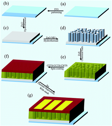 |
| | Fig. 1 Schematic diagram of device structure and its fabrication: (a) ITO-coated glass substrate, (b) ITO patterning, (c) ZnO seed layers, (d) array of ZnO nanorods, (e) ZnS coated ZnO nanorods, (f) deposition of absorber layer (CFTS/CCTS/CNTS) on ZnS coated ZnO nanorods, (g) complete proposed device structure with top layer Au. | |
3. Characterization
A Bruker D8 X-ray diffractometer (XRD) using monochromatic Cu-Kα radiation with a wavelength of 0.154 nm was used to study the crystal phase and structural properties of the nanostructures and cell. The morphologies of the nanostructures and solar cell device were investigated by using a ZEISS Supra 55 field emission scanning electron microscope (FESEM). Ultraviolet-visible (UV-Vis) absorption spectra were recorded using an Agilent Cary 5000 UV-Vis-NIR double beam spectrophotometer, and band gap values were estimated from Tauc plots of the absorption spectra. Electrochemical measurements were taken using a CHI660C electrochemistry workstation. Here, a three-electrode cell assembly was adopted where Ag/AgCl in saturated KCl (0.197 V versus normal hydrogen electrode, NHE) and a Pt electrode were used as reference and counter electrodes, respectively. A 1 cm2 coated sample (ITO/ZnO/ZnS/CFTS or ITO/ZnO/ZnS/CCTS or ITO/ZnO/ZnS/CNTS) was used as a working electrode for this measurement. The electrolyte was a solution of 0.1 M NaOH. Current–voltage characteristics of the devices were recorded using a Keithley 2450 source meter. To illuminate the devices, a solar simulator with an optical mismatch of 2–3% was used. The simulator was calibrated for AM 1.5 and 100 mW cm−2 light illumination conditions using a standard Si reference solar cell.
4. Results and discussions
4.1 Structural properties and surface morphology
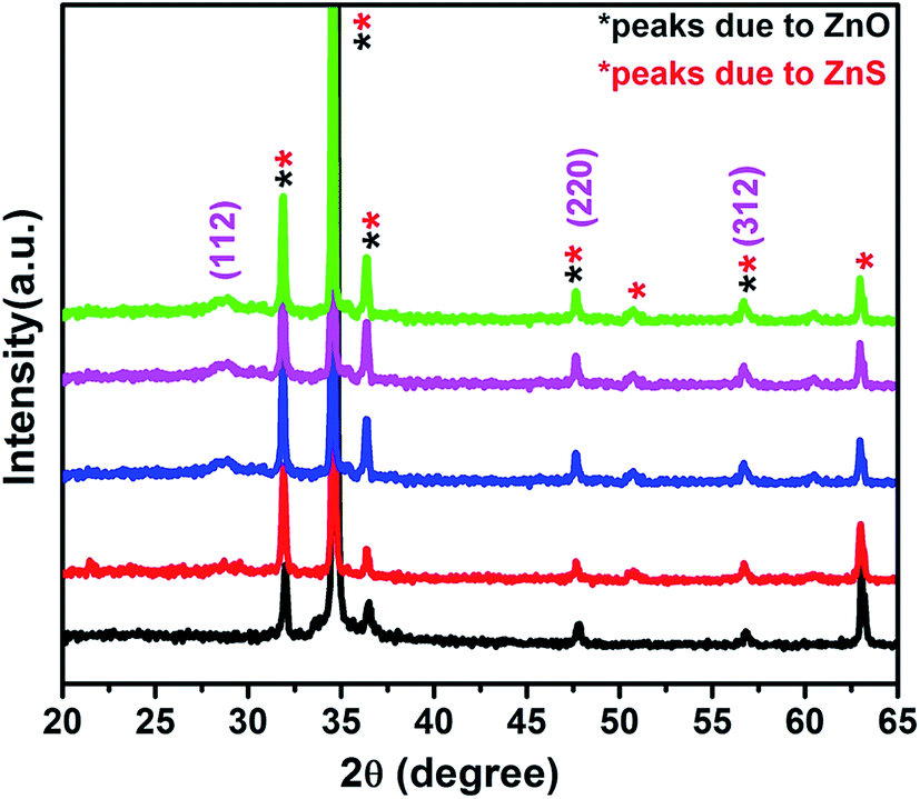
The XRD patterns of the vertically aligned ZnO nanorod, ZnS-coated ZnO nanorod, ITO/ZnO/ZnS/CFTS, ITO/ZnO/ZnS/CCTS and ITO/ZnO/ZnS/CNTS are shown in Fig. 2. The crystallographic characteristics of the ZnO nanorods demonstrated their hexagonal wurtzite structure. The high intensity of the XRD peak at the (002) plane at an angle 2θ = 34.59° confirmed the preferential growth of the nanorods along the c-axis (JCPDS 36-1451). The XRD pattern of ZnO nanorod was fitted using standard program XRDA 3.1 and the lattice parameters ‘a’ and ‘c’ were calculated to be 3.23 Å and 5.16 Å, respectively. The hexagonal ZnS peaks were matched with JCPDS 36-1450. These results confirmed that the coated shell layers on the ZnO nanorods were composed of ZnS. The peaks corresponding to the CFTS, CCTS and CNTS lattice planes were not discerned due to the high intensities of the ZnO peaks, as is clearly shown in the magnified y-axis plot (see S1a†). Only the peak corresponding to the (112) lattice plane of CFTS, CCTS and CNTS was observed in the magnified y-axis plot of the sample; other peaks overlapped with the ZnO/ZnS peaks. To confirm the structural or phase properties of CFTS, CCTS and CNTS, separate thin films of CFTS, CCTS and CNTS were grown on respective glass substrates under identical thin film processing conditions. Fig. S1b of ESI† shows the XRD patterns of CFTS, CCTS and CNTS thin films only; the diffraction peaks at 2θ (degree) values of 28.79, 33.77 and 47.53 (for CFTS); 28.79, 33.69 and 47.70 (for CCTS) and 28.79, 33.61, 47.61 (for CNTS) were assigned to the (112), (200) and (220) planes of the kesterite phase. Our interpretation is in good agreement with reference kesterite phase of JCPDS 26-0575 and previous reports.10 Additionally, to check the impurity phases in CFTS, CCTS and CNTS films, room temperature Raman spectra were recorded and are shown in Fig. S2.† The peaks at 331.58 cm−1 (for the CFTS thin film), 325 cm−1 (for CCTS) and 330.63 cm−1 (for CNTS)23 corresponded to the A1 symmetric vibrational motion of sulfur atoms in these thin films2,18,23 Furthermore, the second-most intense Raman peaks at 284.9 cm−1 (for CFTS), 289 cm−1 (for CCTS) and 284 cm−1 (for CNTS) confirmed the kesterite structure of these thin film samples.19,29
 |
| | Fig. 2 XRD patterns of ZnO nanorod arrays (black line), ZnS-sensitized ZnO (red line), and ITO/ZnO/ZnS/CFTS (blue line), ITO/ZnO/ZnS/CCTS (green line) and ITO/ZnO/ZnS/CNTS (pink line) films. | |
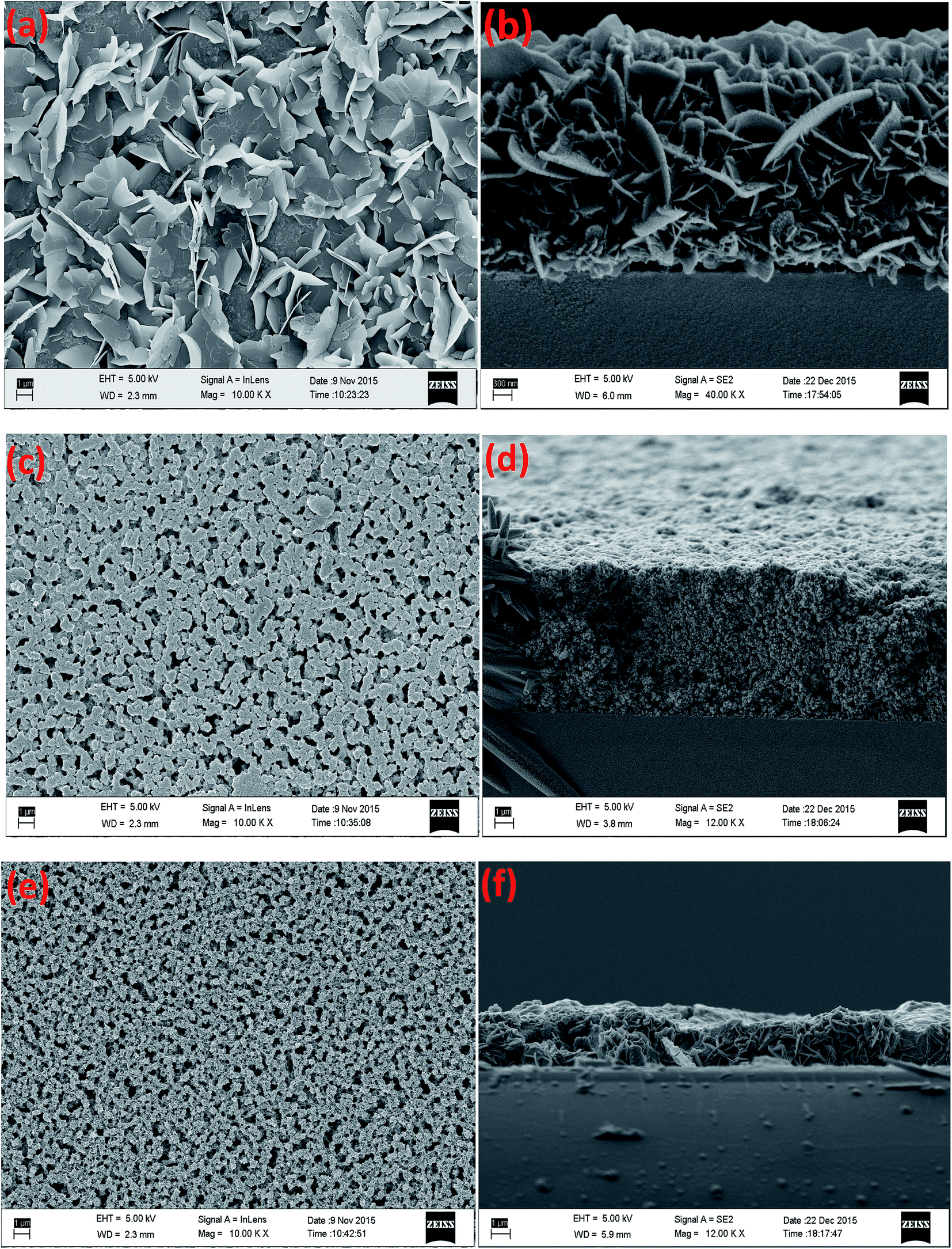
Fig. 3 shows the surface and cross-sectional FESEM views of the ZnO nanorod arrays and ZnO-sensitized ZnS film respectively. The ZnO nanorod arrays were well-aligned and grown nearly vertical (Fig. 3a and insets of Fig. 3a). The distributions of the diameters and thicknesses of the nanorods were estimated using ImageJ software. The diameters of the nanorods were found to be in the range of 200–310 nm and the thicknesses of ZnO NRs (Fig. 3c) were approximately 1.2 μm. The ZnS shell coating layer covered the surface of the nanorods (as shown in Fig. 3b and its insets in the magnified view). A cross-sectional FESEM image of the ITO/ZnO/ZnS sample is shown in Fig. 3d. The surface and cross-sectional views of the FESEM morphologies of ITO/ZnO/ZnS/CFTS, ITO/ZnO/ZnS/CCTS and ITO/ZnO/ZnS/CNTS films are shown in Fig. 4. The thicknesses of these three structures were calculated from their images in Fig. 4b, d and f using ImageJ software and found to be ∼3.2 μm, 3.0 μm, and 3.1 μm, respectively.
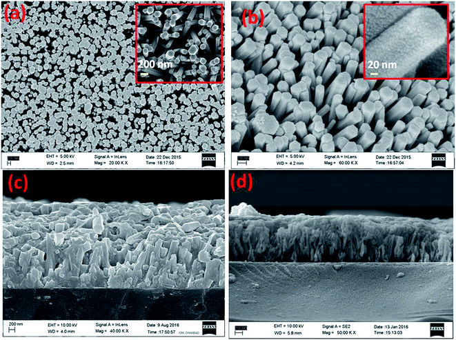 |
| | Fig. 3 (a and b) FESEM images of ZnO nanorod arrays, ZnS sensitized ZnO nanorods; (c and d) cross-sectional image of ZnO nanorod arrays and ZnS sensitized ZnO nanorods. The inset in panel (a) shows ZnO nanorod arrays and the inset in panel (b) shows a magnified view. | |
 |
| | Fig. 4 (a, c and e) Top view and (b, d and f) cross-sectional view FESEM images of ITO/ZnO/ZnS/CFTS, ITO/ZnO/ZnS/CCTS, and ITO/ZnO/ZnS/CNTS films, respectively. | |
4.2 Optical study
Ultraviolet-visible (UV-Vis) spectroscopy measurements were taken to study the optical properties of the kesterite CFTS, CCTS and CNTS thin films, vertically aligned ZnO nanorod, ZnS coated ZnO, ITO/ZnO/ZnS/CFTS, ITO/ZnO/ZnS/CCTS and ITO/ZnO/ZnS/CNTS. Fig. 5 shows the optical absorption spectra of ZnO NRs and the ZnS shell layer coating on the ZnO NRs, as well as of the ITO/ZnO/ZnS/CFTS, ITO/ZnO/ZnS/CCTS and ITO/ZnO/ZnS/CNTS films respectively. The deposition of ZnS on ZnO increased the visible light absorption of the core/shell NRs, due to the optimization of the band gap energy of ZnS (3.18 eV). The enhancement of the light absorption occurred at the well-aligned ZnO nanostructured interface, due to the deposition of the absorber layers. The estimated band gap values (from Tauc plots) of the ZnO NRs and ITO/ZnO/ZnS, as well as of the CFTS, CCTS and CNTS thin films were 3.22 eV, 3.18 eV, 1.87 eV, 1.57 eV and 1.74 eV, respectively (shown in Fig. S2(a–e)†).23 The absorption spectra of the CFTS, CCTS and CNTS thin films are shown in ESI (Fig. S3†).23 Our band gap values calculated using Tauc plots from the experimentally determined UV-Vis spectra are in good agreement with those of previous reports.2,16–22
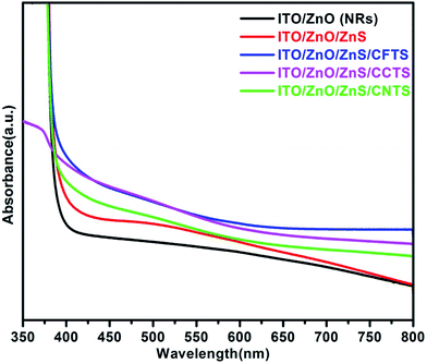 |
| | Fig. 5 Absorption spectra of the ZnO nanorod and ZnS-sensitized ZnO nanorod, and of the ITO/ZnO/ZnS/CFTS, ITO/ZnO/ZnS/CCTS and ITO/ZnO/ZnS/CNTS films. | |
4.3 Electrical properties
4.3.1 Impedance and cyclic voltammetry measurements.
Electrochemical impedance spectroscopy (EIS) analysis was performed in the dark and under visible light illumination. The impedance spectra were obtained in the frequency range 100 kHz to 10 mHz with an AC amplitude of 5 mV. Fig. 6 shows the Nyquist plots for ITO/ZnO/ZnS/CFTS, ITO/ZnO/ZnS/CCTS and ITO/ZnO/ZnS/CNTS electrodes with respect to the platinum (Pt) cathode in the dark and under visible light illumination. All of the related impedance data were obtained from a circuit (shown in the inset of Fig. 6) equivalent to that described in the literature. Our measured impedance curves in the Nyquist plot can be well-fitted with this circuit, which consisted of four resistances (Rs, Rd, Rct and Rf), a capacitance and two constant phase elements (Q). Here, Rs is related to the internal resistance, which includes the intrinsic electrode resistance, i.e., the resistance of the electrolyte and that of the contact between the electrode and current collector; and Rd is the diffuse layer resistance, Rct is the charge transfer resistance, and Rf is the film resistance. The total resistance is the sum of Rs, Rd, Rct and Rf, and may be due to the charge recombination, specific area, morphology and crystallinity of the working electrode.25,30,31 The impedance parameters were analysed from least-squares fits to the above equivalent circuit by using ZSimpWin 3.22d software. The fitted Rs, Rd, Rct, Rf parameters and total resistance from the Nyquist plots are summarized in Table 1. The EIS Nyquist plots for all thin films in the dark and under visible light irradiation indicated good charge transfer across the solid electrolyte interfaces.
 |
| | Fig. 6 Nyquist plots of the ITO/ZnO/ZnS/CFTS, ITO/ZnO/ZnS/CCTS and ITO/ZnO/ZnS/CNTS samples in the dark and under visible light illumination. | |
Table 1 Impedance parameters obtained from the equivalent circuit for ITO/ZnO/ZnS/CFTS, ITO/ZnO/ZnS/CCTS and ITO/ZnO/ZnS/CNTS samples in the dark and under visible light illumination
| Sample |
Condition |
R
s (Ω) |
R
d (Ω) |
R
ct (Ω) |
R
f (Ω) |
Total resistance (Ω) TR = Rs + Rd + Rct + Rf |
| ITO/ZnO/ZnS/CFTS |
Dark (D) illumination (L) |
4.15 |
12.33 |
2709 |
400.4 |
3125.88 |
| 7.77 |
11.06 |
817.2 |
307.9 |
1143.93 |
| ITO/ZnO/ZnS/CCTS |
Dark (D) illumination (L) |
3.80 |
351.9 |
2098 |
177.7 |
2631.40 |
| 3.63 |
9.612 |
1430 |
9.34 |
1452.58 |
| ITO/ZnO/ZnS/CNTS |
Dark (D) illumination (L) |
4.76 |
14.12 |
1864 |
980 |
2862.88 |
| 5.06 |
9.21 |
456.5 |
12.79 |
483.56 |
To investigate the electrocatalytic activities of the ITO/ZnO/ZnS/CFTS, ITO/ZnO/ZnS/CCTS and ITO/ZnO/ZnS/CNTS electrodes, cyclic voltammetry (CV) was carried out in a three-electrode system with 0.1 M NaOH electrolyte solution in the potential range −1.5 to +0.5 V with respect to an Ag/AgCl reference electrode and with scan rates ν of 5, 25, 50 and 100 mVs−1. The functioning of a photoelectrochemical cell (PEC) is fundamentally based on the junction between the component semiconductor and electrolyte, where the electrolyte is used for charge transfer between the photoelectrode and counter electrode.32 The cyclic voltammogram curves of all of the samples displayed obvious cathodic peaks (Fig. 7a–c). All of the device structures showed an enhancement of current density values when illuminated with visible light. These copper chalcogenide thin film solar cell device structures can be used in photoelectrochemical cell applications.
 |
| | Fig. 7 Cyclic voltammograms for (a) ITO/ZnO/ZnS/CFTS, (b) ITO/ZnO/ZnS/CCTS and (c) ITO/ZnO/ZnS/CNTS at scan rates ν of 5, 25, 50, and 100 mV s−1 in the dark (D) and under visible light (L) illumination using a Pt electrode as a counter electrode. | |
4.3.2 Current density–voltage characteristics.
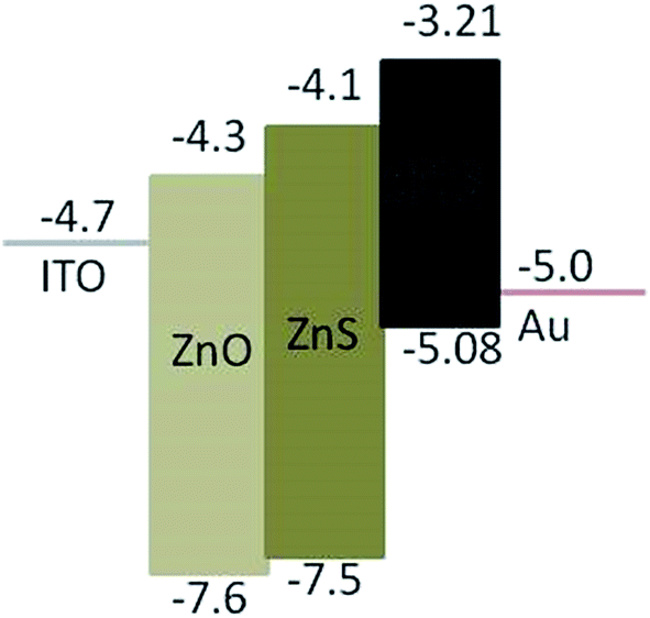
The photovoltaic performances of the samples were also evaluated under irradiation of AM 1.5, and the results are shown in Fig. 9. The energy band diagram of the device with the ITO/ZnO/ZnS/CFTS/Au architecture is shown in Fig. 8, whereas those of ITO/ZnO/ZnS/CCTS/Au and ITO/ZnO/ZnS/CNTS/Au are shown in Fig. S4 (in ESI†). Here, ZnO nanorods functioned as the electron-transport layer because their work function matched well with the acceptors and because of their high electron mobility. A ZnS layer was added to optimize the alignment between the energy band of the absorption layer and that of the ZnO layer, to reduce the density of surface defects at the interface, and to increase the lifetime of the charge carriers. The active area of each device was estimated to be 0.12 cm2. The solar cell device fabricated with the CFTS photoactive layer (ITO/ZnO/ZnS/CFTS/Au) exhibited a short-circuit current density (JSC) of 7.50 mA cm−2, open-circuit voltage (VOC) of 0.75 V (as shown in Fig. 9), and fill factor (FF) of 0.486, and yielded a 2.73% power conversion efficiency (η) under illumination. Those with the ITO/ZnO/ZnS/CCTS/Au configuration showed an efficiency (η) of 3.23% with VOC = 0.77 V, JSC = 7.83 mA cm−2 and FF = 0.537, and that with the configuration ITO/ZnO/ZnS/CNTS/Au yielded η = 2.71% with VOC = 0.75 V, JSC = 6.82 mA cm−2 and FF = 0.531.
 |
| | Fig. 8 Energy band diagram of the ITO/ZnO/ZnS/CFTS/Au device structure. | |
 |
| | Fig. 9
J–V characteristics of the devices with the configurations ITO/ZnO/ZnS/CFTS/Au, ITO/ZnO/ZnS/CCTS/Au and ITO/ZnO/ZnS/CNTS/Au under 100 mW cm−2 illumination conditions. | |
As indicated above, the device with the CFTS photoactive layer exhibited an FF of ∼0.487 whereas the devices with CCTS and CNTS showed FF values of ∼0.538 and 0.531, respectively. Basically, the FF factor of such devices is dependent on the shunt (RS) and series resistance (RSH) of the device, where both RS and RSH are in turn dependent on the quality of the films and charge transport/trap levels in the devices. Denser photoactive layer films generally provide better pathways for charge transport. After condensation, the CFTS thin film formed flake-like structures (Fig. 4a and b) after condensation. These structures increased the grain boundaries, and this increase may have increased the number of recombination centers. This morphology may have also hindered the flow of charge carriers, and may have caused the relatively high value of RS, low value of RSH, and hence low value of FF in the devices with CFTS. In contrast to the CFTS films, the CCTS and CNTS films showed dense and compact morphologies, which apparently led to the relatively high FF values for the devices with CCTS and CNTS. These interpretations are in good agreement with impedance parameters (charge transfer resistance and total resistance) obtained from the equivalent circuits for the ITO/ZnO/ZnS/CFTS, ITO/ZnO/ZnS/CCTS and ITO/ZnO/ZnS/CNTS samples in the dark and under visible light illumination (Table 1).
The CCTS-based device showed a better PV performance than did the devices with CFTS and CNTS. The better PCE of the devices with the CCTS photoactive layer may have been due to its band gap (1.57 eV) and appropriate valence band (VB) position (5.2 eV). Its band gap allowed for absorption of a wide range of the solar spectrum. And the VB position close to the Au work function (5.0 eV) may have offered better charge collection, and this better charge collection would help explain the improvement in FF. Due to lack of previous reported CFTS, CCTS and CNTS based devices on metal oxide nanostructures, the photovoltaic performances of our present devices cannot be compared. However, the photovoltaic performance results of our current devices were remarkable in that they were comparable to previously reported performances of CZTS inorganic solar cells on metal oxide nanostructures.3,10,13–15,24,25,33 Also, our proposed devices yielded a better photovoltaic performance than did the previously reported CFTS device (Al:ZnO/ZnO/CdS/CFTS/Mo/glass).28 Therefore, we strongly believe that the results of present work may offer the good and fruitful possibility to understand the copper quaternary chalcogenides based low-cost thin film inorganic photovoltaic power conversion cells.
5. Conclusions
In summary, the solution-based method for synthesis, structural, optical and electrical properties of kesterite phase CFTS, CCTS and CNTS thin film solar cell using ZnS coated ZnO nanorod arrays for the first time have been investigated. The approximate thickness of ITO/ZnO/ZnS/CFTS/Au, ITO/ZnO/ZnS/CCTS/Au and ITO/ZnO/ZnS/ CNTS/Au superstrate structure is 3.2 μm, 3.0 μm and 3.1 μm respectively. These solar cell devices exhibit an efficiency of 2.73%, 3.23% and 2.71% respectively under 100 mW cm−2 illuminations. Further, the good charge transformation between solid electrolyte interfaces has been analysised by EIS Nyquist plot of all the thin film device structures under dark and visible light irradiation. The method proposed here can serve as a useful approach for fabricating CFTS, CCTS and CNTS based solar cell devices on metal oxide nano structures and photo electrochemical cells.
Acknowledgements
Authors A.G. and R.T. gratefully acknowledge the Indian Institute of Technology (Indian School of Mines), Dhanbad, India for financial support and for use of the Central Research Facility. The author R. T. thanks the Department of Science and Technology for grant no. SR/FTP/PS-184/2012, SERB vide Dy.No. SERB/F/5439/2013–14 and Faculty Research Scheme-FRS (54)/2013–2014/APH.
References
- H. Katagiri, N. Sasaguchi, S. Hando, S. Hoshino, J. Ohashi and T. Yokota, Preparation and evaluation of Cu2ZnSnS4 thin films by sulfurization of EB evaporated precursors, Sol. Energy Mater. Sol. Cells, 1997, 49, 407–414 CrossRef CAS.
- K. Mokurala, S. Mallick and P. Bhargava, Alternative quaternary chalcopyrite sulfides (Cu2FeSnS4 and Cu2CoSnS4) as electrocatalyst materials for counter electrodes in dyesensitized solar cells, J. Power Sources, 2016, 305, 134–143 CrossRef CAS.
- K. Tanaka, M. Kurokawa, K. Moriya and H. Uchiki, Surface morphology improvement of three-dimensional solar cell with Cu2ZnSnS4 absorber, J. Alloys Compd., 2013, 571, 98–102 CrossRef CAS.
- A. Ghosh, R. Thangavel and M. Rajagopalan, First principles study of electronic and optical properties of Cu2ZnSnX4 (X = S, Se) solar absorbers by Tran-Blaha-modified Beckee Johnson potential approach, J. Mater. Sci., 2013, 48, 8259–8267 CrossRef CAS.
- B. J. Li, P. F. Yin, Y. Z. Zhou, Z. M. Gao, T. Ling and X. W. Du, Single crystalline Cu2ZnSnS4 nanosheet arrays for efficient photochemical hydrogen generation, RSC Adv., 2015, 5, 2543–2549 RSC.
- Y. Cui, R. Deng, G. Wang and D. Pan, A general strategy for synthesis of quaternary semiconductor Cu2MSnS4 (M = Co2+, Fe2+, Ni2+, Mn2+) nanocrystals, J. Mater. Chem., 2012, 22, 23136–23140 RSC.
- A. Ghosh, R. Thangavel and M. Rajagopalan, First-principles study of structural stability and optical properties of Cu2XSnY4 (X = Fe, Co, Ni; Y = S, Se) for photovoltaic applications, Energy and Environmental Focus, 2014, 3, 142–151 CrossRef.
- T. You, L. Jiang, K. L. Han and W. Q. Deng, Improving the performance of quantum dot-sensitized solar cells by using TiO2 nanosheets with exposed highly reactive facets, Nanotechnology, 2013, 24, 245401–245406 CrossRef PubMed.
- J. W. Cho, S. J. Park, J. Kim, W. Kim, H. K. Park, Y. R. Do and B. K. Min, Bulk heterojunction formation between indium tin oxide nanorods and CuInS2 nanoparticles for inorganic thin film solar cell applications, ACS Appl. Mater. Interfaces, 2012, 4, 849–853 CAS.
- D. Lee and K. Yong, Solution-processed Cu2ZnSnS4 superstrate solar cell using vertically aligned ZnO nanorods, Nanotechnology, 2014, 25, 065401–065408 CrossRef PubMed.
- D. Lee and K. Yong, Superstrate CuInS2 photovoltaics with enhanced performance using a CdS/ZnO nanorod array, ACS Appl. Mater. Interfaces, 2012, 4, 6758–6765 CAS.
- J. W. Cho, S. J. Park, W. Kim and B. K. Min, Fabrication of nanocrystal ink based superstrate-type CuInS2 thin film solar cells, Nanotechnology, 2012, 23, 265401–265406 CrossRef PubMed.
- Q. Chen, S. Cheng, S. Zhuang and X. Dou, Cu2ZnSnS4 solar cell prepared entirely by non-vacuum processes, Thin Solid Films, 2012, 520, 6256–6261 CrossRef CAS.
- M. Kurokawa, K. Tanaka, K. Moriya and H. Uchiki, Fabrication of three-dimensional-structure solar cell with Cu2ZnSnS4, Jpn. J. Appl. Phys., 2012, 51, 10NC33 CrossRef.
- Q. M. Chen, Z. Q. Li, Y. Ni, S. Y. Cheng and X. M. Dou, Doctor-bladed Cu2ZnSnS4 light absorption layer for low-cost solar cell application, Chin. Phys. B, 2012, 21, 038401–038407 CrossRef.
- C. L. Yang, Y. H. Chen, M. Lin, S. L. Wu, L. Li, W. C. Liu, X. S. Wu and F. M. Zhang, Structural, optical and magnetic properties of Cu2NiSnS4 thin films deposited by facile one-step electro deposition, Mater. Lett., 2016, 166, 101–104 CrossRef CAS.
- X. Zhang, N. Bao, B. Lin and A. Gupta, Colloidal synthesis of wurtzite Cu2CoSnS4 nanocrystals and the photoresponse of spray-deposited thin films, Nanotechnology, 2013, 24, 105706–105708 CrossRef PubMed.
- D. B. Khadka and J. H. Kim, Structural, optical and electrical properties of Cu2FeSnX4 (X = S, Se) thin films prepared by chemical spray pyrolysis, J. Alloys Compd., 2015, 638, 103–108 CrossRef CAS.
- B. Murali, M. Madhuri and S. B. Krupanidhi, Solution Processed Cu2CoSnS4 Thin Films for Photovoltaic Applications, Cryst. Growth Des., 2014, 14, 3685–3691 CAS.
- H.-J. Chen, S-W Fu, T-C Tsai, C-F Shih, Quaternary Cu2NiSnS4 thin films as a solar material prepared through electrodeposition, Mater. Lett., 2016, 166, 215–218 CrossRef CAS.
- M. K. Gonce, E. Aslan, F. Ozel and I. H. Patir, Dye-Sensitized Cu2XSnS4 (X = Zn, Ni, Fe, Co, and Mn) Nanofibers for Efficient Photocatalytic Hydrogen Evolution, ChemSusChem, 2016, 9, 600–605 CrossRef CAS PubMed.
- J.-Y. Park, J. H. Noh, T. N. Mandal, S. H. Im and Y. Jun, Sang Il Seok, Quaternary semiconductor Cu2FeSnS4 nanoparticles as an alternative to Pt catalysts, RSC Adv., 2013, 3, 24918–24921 RSC.
- A. Ghosh, A. Biswas, R. Thangavel and G. Udayabhanu, Photo-electrochemical property and electronic band structure of kesterite copper chalcogenides Cu2-II-Sn-S4 (II = Fe, Co, Ni) thin films, RSC Adv., 2016, 6, 96025–96034 RSC.
- S. Suehiro, K. Horita, K. Kumamoto, M. Yuasa, T. Tanaka, K. Fujita, K. Shimanoe and T. Kida, Solution-processed Cu2ZnSnS4 nanocrystal solar cells: efficient stripping of surface insulating layers using alkylating agents, J. Phys. Chem. C, 2014, 118, 804–810 CAS.
- Y. Hou, H. Azimi, N. Gasparini, M. Salvador, W. Chen, L. S. Khanzada, M. Brandl, R. Hock and C. J. Brabec, Low-temperature solution-processed kesterite solar cell based on in situ deposition of ultrathin absorber layer, ACS Appl. Mater. Interfaces, 2015, 7, 21100–21106 CAS.
- R. R. Prabhakar, N. H. Loc, M. H. Kumar, P. P. Boix, S. Juan, R. A. John, S. K. Batabyal and L. H. Wong, Facile water-based spray pyrolysis of earth-abundant Cu2FeSnS4 thin films as an efficient counter electrode in dye-sensitized solar cells, ACS Appl. Mater. Interfaces, 2014, 6, 17661–17667 CAS.
- E. Ha, L. Y. Suk Lee, H.-W. Man, S. C. E. Tsang and K.-Y. Wong, Morphology-controlled synthesis of Au/Cu2FeSnS4 core-shell nanostructures for plasmon-enhanced photocatalytic hydrogen generation, ACS Appl. Mater. Interfaces, 2015, 7, 9072–9077 CAS.
- X. Meng, H. Deng, J. Tao, H. Cao, X. Li, L. Sun, P. Yang and J. Chu, Heating rate tuning in structure, morphology and electricity properties of Cu2FeSnS4 thin films prepared by sulfurization of metallic precursors, J. Alloys Compd., 2016, 680, 446–451 CrossRef CAS.
- X. Lu, Z. Zhuang, Q. Peng and Y. Li, Wurtzite Cu2ZnSnS4 nanocrystals: a novel quaternary semiconductor, Chem. Commun., 2011, 47, 3141–3143 RSC.
- P. A. Fernandes, A. F. Sartori, P. M. P. Salome, J. Malaquias, A. F. da Cunha, M. P. F. Grac and J. C. Gonzalez, Admittance spectroscopy of Cu2ZnSnS4 based thin film solar cells, Appl. Phys. Lett., 2012, 100, 233504 CrossRef.
- E. Kask, J. Krustok, S. Giraldo, M. Neuschitzer, S. Lopez-Marino and E. Saucedo, Temperature dependent electrical characterization of thin film Cu2ZnSnSe4 solar cells, J. Phys. D: Appl. Phys., 2016, 49, 085101–085106 CrossRef.
- C. D. Lokhande and S. H. Pawar, Electrochemical photovoltaic cells for solar energy conversion, Mater. Chem. Phys., 1984, 11, 201–277 CrossRef CAS.
- A. Ghosh, R. Thangavel and A. Gupta, Solution-processed Cd free kesterite Cu2ZnSnS4 thin film solar cells with vertically aligned ZnO nanorod
arrays, J. Alloys Compd., 2017, 694, 394–400 CrossRef CAS.
Footnote |
| † Electronic supplementary information (ESI) available. See DOI: 10.1039/c6ra24149b |
|
| This journal is © The Royal Society of Chemistry 2016 |
Click here to see how this site uses Cookies. View our privacy policy here.