DOI:
10.1039/C6RA23729K
(Paper)
RSC Adv., 2016,
6, 115335-115344
Synthesis of Te-doped ZnO nanowires with promising field emission behavior
Received
23rd September 2016
, Accepted 2nd December 2016
First published on 2nd December 2016
Abstract
In the current study, a successful synthesis of ZnO nanowire films doped with Te was performed through electrodeposition on the zinc foil followed by annealing in air for 4 hours at 400 °C. The conditions for growth were chosen as the concentrations of electrolyte and deposition time. The XRD patterns for the post-annealed samples are shown as a set of well-specified diffraction peaks relating to the ZnO wurtzite phase. The growth conditions impact the surface morphologies of the as-prepared films. Upon annealing, the ZnO nanowire formation was observed for shorter deposition times. The incorporation of Te ions into the ZnO lattice was confirmed using X-ray and Auger photoelectron spectroscopy. The diverse emission bands originating from different transition mechanisms were evaluated through photoluminescence and Raman studies. In the field emission studies, the best threshold field values, which are necessary for drawing an emission current density of ∼100 μA cm−2, are 2.13 V μm−1 for T1S1 and 2.42 V μm−1 for T1S2. The post-annealed film with a lower concentration of wires shows an excellent emission current stability at the preset value of ∼10 μA over 4 hours. The results show that Te ions play a key role in controlling the morphologies, resulting in various morphologies and densities of the ZnO wires, which have different field emission features. This technique may have a potential to produce electron sources for high current density applications.
1. Introduction
Field emission is a key aspect of nanoscale materials, and it has been extensively investigated because it is important for both fundamental studies and device applications. Obtaining high current density in a low electric field is important for developing field emission cathodes. Two approaches, tailoring the emitter geometry and modifying the electronic properties, can be used to achieve this purpose. The first method has several restrictions in the preparation of anisotropic nanostructures with very fine apex radii. Furthermore, attaining the desired feature is difficult with the second method because the chemical reactivity may decrease the emission performance of the cathodes. Consequently, a suitable hybrid of two approaches is considered as a useful alternative for achieving better field emission performance, and this method has been successfully applied by several researchers.
Wide-band-gap semiconductors have been extensively studied because of their unique optical and electrical features. One of the metal-oxide materials, which is greatly used in the synthesis of nanostructures, is ZnO. This metal oxide has been applied in various areas, including optoelectronics, nanotechnology, and spintronics, because of its wide direct band gap (3.37 eV) and large exciton binding energy (60 meV).1 Therefore, many reports have been recently published on the low-dimensional ZnO structures, including nanoparticles,2 rods,3 tubes,4 marigolds/multipods,5 belts,6 rings,7 helixes/springs,8 and combs,9 enabling unique size and shape dependent features. Among these structures, the best candidate for achieving high field electron emission in a low-electric field is one-dimensional (1-D) nanostructures because of their high aspect ratios, low work functions, and conductivities.10 Different approaches, such as thermal oxidation,11 chemical vapor deposition,12 catalysis-driven molecular beam epitaxy,13 thermal evaporation,14 and electrochemical deposition,15,16 have been used to synthesize these ZnO nanostructures with high selectivity and yield in both powder and thin film forms. Furthermore, doping ZnO with selective elements suggests that this is an efficient method because it generates nanostructures with good electrical, optical, and magnetic features, which are essential for their practical applications.17–21 An appropriate method for doping ZnO nanostructures is required for the widespread applications of ZnO nanostructures in nanoscale electronic and photonic devices.
The structural, surface morphological, chemical, optical, and field emission features of the ZnO nanostructures doped with Te, prepared through the cathodic electrodeposition on a zinc substrate and an annealing procedure (thermal oxidation), are reported in the current study for the first time. The impact of the amount of Te on the physical features was studied to understand the field emissions of these films. According to the field emission measurements, the threshold field values needed to draw an emission current density of ∼100 μA cm−2 are 2.13 V μm−1 for the post-annealed T1S1 sample and 2.42 V μm−1 for the post-annealed T1S2 sample. Moreover, these Te-doped ZnO nanowire emitters show excellent emission current constancies at the preset value of ∼10 μA over six hours.
2. Experimental methods
2.1. Synthesis and deposition of the nanostructured thin films
A thin film of the ZnO nanostructures doped with Te was synthesized in a conventional three-electrode cell in an aqueous solution with a supporting electrolyte comprising a combination of Zn(NO3)·2H2O and TeO2. Depositions were performed at various levels and intervals to achieve various concentrations of Te as a dopant. The synthesis conditions are given in Table 1. The temperature was maintained at 80 ± 2 °C during all deposition tests. The working, counter, and reference electrodes used in all the deposition tests were polycrystalline Zn foil (purity ∼ 99.99%, Alfa Aesar), a platinum sheet, and a saturated calomel electrode (SCE, E0 = 0.244 V), respectively. Before all electrodeposition tests, Zn foil and platinum electrode were ultrasonically washed with acetone and methanol for 10 minutes each. The condition of cathodic polarization was maintained at −1 V with respect to the SCE using a computer controlled electrochemical analyzer (Model-1100A Series, CH Instruments, USA). The electrolyte was continually stirred during the synthesis process to achieve uniform mass transfer conditions. The Zn foil (substrate), after the fixed deposition time, was removed from the electrolyte, immersed in distilled water, and dried in air. In all cases, annealing of the “as-prepared” thin films was performed at ∼400 °C in air for 4 hours. At least three samples were prepared under similar experimental conditions, and their characterization was performed using different analytical methods to verify the reproducibility and repeatability of the results.
Table 1 Synthesis parameters of the Te–ZnO thin films
| Sample |
Precursor materials (mM) |
Deposition time (min) |
| Zn(NO3)·2H2O |
TeO2 |
| T1S1 |
10 |
1 |
10 |
| T1S2 |
50 |
5 |
| T2S1 |
10 |
1 |
30 |
| T2S2 |
50 |
5 |
2.2. Characterization of the materials
An X-ray diffractometer (XRD, Model-D8, Advance, Bruker AXS, Cu anode, Kα = 1.5406 Å) and scanning electron microscope (SEM, JEOL, JSM-6360A) were used to characterize the samples. An energy-dispersive X-ray spectrometer (EDS) attached to the SEM and a field emission Auger electron spectrometer (FEAES, JEOL, Jamp-9500F) were applied to determine the elemental compositions of the synthesized materials. The chemical analysis of the deposited films was performed using X-ray photoelectron spectroscopy (XPS, VG Microtech ESCA 3000). The XPS spectra were obtained at a base pressure of 10−10 mbar using Mg-Kα radiation (1253.6 eV, line width 0.7 eV) generated at a power of 150 W. The optical features of the deposited films were studied through room temperature photoluminescence (PL) measurements. A 325 nm wavelength He–Cd laser was applied as the excitation source. The Raman spectra of the thin films were obtained under ambient conditions by a Renishaw InVia system using a green Ar ion laser with an excitation wavelength of 514 nm. The measurements of the field emission current versus applied voltage (I–V) and current versus time (I–t) were performed in a planar diode layout in a vacuum chamber evacuated to a base pressure of ∼1.0 × 10⁻⁸ mbar. The sample was used as the cathode, and the anode was a semi-transparent phosphor screen that was parallel to the cathode with about 1 mm distance between them. The emission current was obtained by changing the DC voltage applied between the cathode and anode with a 40 V step (0–40 kV, Spellman, USA). Special care was taken to prevent any leakage of the current by ensuring appropriate grounding. The reproducibility of the field emission outcomes was checked by studying a minimum of two samples prepared under similar experimental conditions.
3. Results and discussion
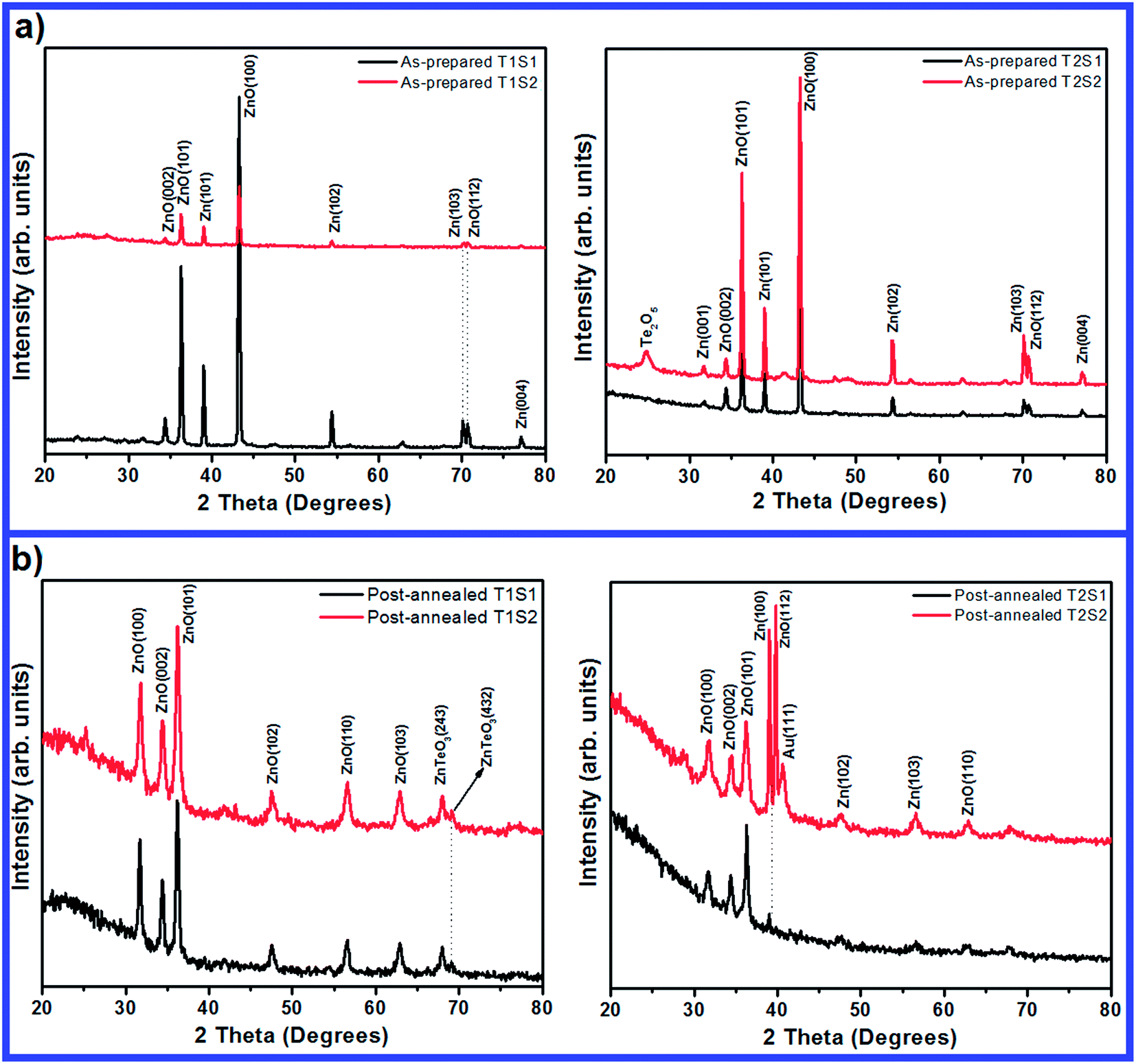
Fig. 1a shows the XRD patterns of the as-prepared samples (T1S1, T1S2, T2S1, and T2S2). A set of peaks relating to Zn and ZnO phases (JCPDS file no. 01-074-0534 and 01-075-1526, respectively) and Te2O5 phase (JCPDS file no. 00-001-1136) appeared in the sample pattern. The diffraction peak of Zn is due to the use of Zn foil as a substrate and the peak corresponding to Te2O5 is only observed at higher concentrations and longer deposition periods (T2S2 sample). Fig. 1b demonstrates the XRD patterns of the post-annealed samples in which several well-defined diffraction peaks corresponding to the wurtzite hexagonal phase of ZnO (JCPDS file no. 00-80-0075) can be observed. The concentration and deposition time affect the general properties of the diffraction patterns relating to the annealed films in all samples. Remarkably, no diffraction peak relating to the TeO2 phase is observed after annealing the as-prepared films. The diffusion of Te atoms into the ZnO lattice and the occupancy of several Te2− at the O2− sites are expected during the annealing. One important point is that in the wurtzite ZnO crystal, the radii of Te and O ions are expected to be r(Te2−) = 2.07 Å and r(O2−) = 1.40 Å. The greater radius of Te ion compared to that of O ion can deform the ZnO lattices. In addition, the XPS analysis shows the substitutional occupancy of Te2− ions at the O2− sites and this is explained in the following sections.
 |
| | Fig. 1 XRD patterns of the (a) as-prepared and (b) post-annealed samples. | |
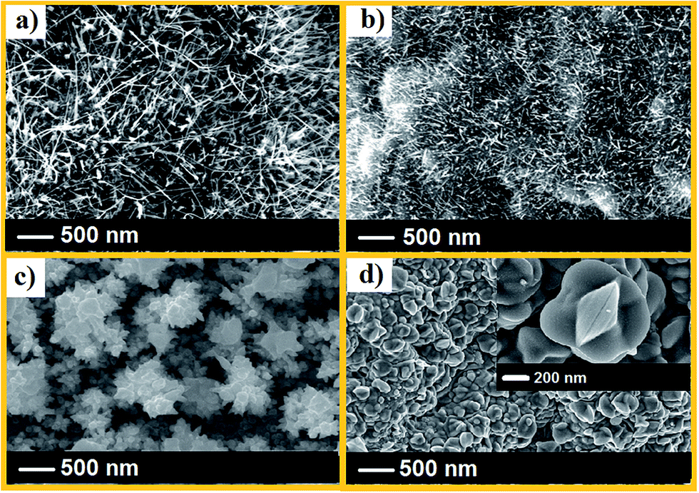
To investigate the impacts of deposition duration and electrolyte concentration, first, the deposition time was chosen and the synthesis was then performed at various electrolyte concentrations under the optimized conditions of deposition. Fig. 2 shows the SEM images of the ‘as-prepared’ samples (T1S1, T1S2, T2S1, and T2S2). The images obviously display that the rate of growth is proportional to the deposition time. A uniform granular morphology on the entire surface of the substrate was observed for the sample, which was deposited for 10 minutes (T1S1, Fig. 1a). An increase in the electrolyte concentration caused agglomeration of the particles to generate larger and uniform-sized grains (T1S2, Fig. 2b). The morphologies of the ZnO thin film in a 30 minutes deposition interval at lower concentration were assembled via particles growing from the central line of the cauliflower-like structures (T2S1, Fig. 2c). Well-defined multidendritic morphologies, containing one stem and small needle-shaped branches symmetrically dispersed on the sides of the stem, are observed upon a closer inspection. The stem lengths are several microns and the diameters of the branches are in the range of 40–125 nm. An increase in the electrolyte concentration causes conversion of the cauliflower-like structures to spherical agglomerated/unassembled particles deposited on the substrate with approximate sizes ranging from 200 nm to 1 μm (T2S2, Fig. 2d). The observed surface morphologies can be attributed to the higher rate of growth because of the presence of more precursors with the increasing deposition time as this fixed potential is related to the growth under limited conditions of diffusion. Fig. 3 demonstrates the post-annealed SEM images of all the samples. Remarkably, the films prepared with shorter deposition times (i.e. T1S1 and T1S2), upon annealing for 4 hours at ∼400 °C in air, showed the generation of ZnO wires on the entire surface of the substrate; the wires are arbitrarily directed and few of them protrude outside the surface of the substrate (Fig. 3a and b). The wire diameters of the post-annealed T1S1 and T1S2 samples are in the range from 10 to 35 nm. The lengths and densities of the ZnO wires are higher in the T1S1 sample as compared to the T1S2 sample. This surface morphology can be ascribed to the higher rate of growth. The post-annealed T1S1 sample had the best aspect ratio. The results of the current study indicated this growth after annealing in air.16,22 The exact result of the images displays that the wires become thicker and shorter and show smaller areal density with the increasing electrolyte concentration. Note that the well-defined multidendritic morphologies of the post-annealed samples were less altered compared to the other morphologies (T2S1, Fig. 3c), whereas in samples with the agglomerated spherical particles, these morphologies changed to grains with multi-blade structures (T2S2, Fig. 3d). This may be because of the energy of the surface of the spherical-shaped particles that results in the formation of arbitrarily oriented multi-blade structures.
 |
| | Fig. 2 SEM images of the as-prepared samples: (a) T1S1, (b) T1S2, (c) T2S1, and (d) T2S2. | |
 |
| | Fig. 3 SEM images of the post-annealed samples: (a) T1S1, (b) T1S2, (c) T2S1, and (d) T2S2. | |
EDS was applied to analyze the chemical purities and stoichiometries of the as-prepared and post-annealed films (the EDS spectra are not shown here). The outcomes proved that the as-prepared films only contained Zn, O, and Te elements. The mean values of the post-annealed films were determined and a comparison of the data for all the samples is given in Table 2. In the samples, better stoichiometry is observed at lower values of Te atomic percentage compared to higher values. This finding is in excellent accordance with the prior outcomes on the impact of oxygen passivation on the structure of ZnO, where the O vacancies are decreased.17
Table 2 EDS results of the post-annealed Te–ZnO nanostructures grown under different growth conditions
| Annealed sample |
Atomic percentage (at%) (average) |
| Zn |
O |
Te |
| T1S1 |
48.93 |
50.90 |
0.17 |
| T1S2 |
53.72 |
41.52 |
4.75 |
| T2S1 |
49.28 |
50.25 |
0.47 |
| T2S2 |
57.67 |
37.17 |
5.17 |
The XPS method was used to analyze the chemical compositions of the samples. This method can offer a quantitative elemental analysis of the elements within a few nanometers of a film's surface. The XPS spectra of the post-annealed T1S1 sample are shown in Fig. 4. The core level photoemission peaks relating to Zn, O, Te, and C could only be observed in the survey scan spectrum shown in Fig. 4a. Therefore, the sample purity was proved within the sensitivity range of the method. The C-1s photoemission peak at 285.0 eV was used as an internal reference to correct the locations of all peaks. Fig. 4b demonstrates a detailed scan of the Zn-2p region. The Zn-2p3/2 peak is observed at 1021.2 eV and a peak relating to Zn-2p1/2 appears at 1044.2 eV with a spin orbit splitting of 23.0 eV; this confirms the fully oxidized state of the Zn species.23 The symmetric peak does not correspond to any other species including metallic zinc, whose related peak would have appeared as a shoulder at ∼1021.1 eV. Fig. 4c demonstrates the core level photoemission peak related to the O-1s region. The displayed peak at 530.3 eV is ascribed to the oxidized metal ions of the films called O–Zn in the ZnO lattice. As observed in Fig. 4d, the binding energies of Te-3d5/2 and Te-3d3/2 are 576 eV and 586.4 eV, respectively. This observation demonstrates the incorporation of a Te dopant into the lattice of ZnO. The substitutional doping of Te ions into the ZnO lattice can be proved as there is no TeO2 phase in the XRD pattern. Some amounts of carbon were observed in the sample along with zinc and oxygen, which could be due to the treatment of the sample and migration of several carbons from the filaments in the vacuum system. This outcome is in accordance with the EDS analysis results.
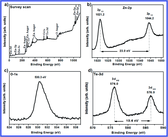 |
| | Fig. 4 XPS spectra of the post-annealed T1S1 sample: (a) survey scan, (b) Zn spectrum, (c) O spectrum, and (d) Te spectrum. | |
The XPS and EDX results were supported by the field emission Auger electron spectroscopy (FEAES). Fig. 5 displays the high resolution N(E) Auger electron spectra of Te, O, and Zn for a single nanowire. The peaks observed at 402 eV and 473 eV are related to Te (MNN), the peaks observed at 506 eV are related to O (KLL), and the peaks at 819, 894, 981, and 1004 eV are associated with Zn (LMM). The peak of ZnO wires has a slight shift compared to that of the doped ZnO wires. This shift in the Auger electron energy occurs in In-doped ZnO nanowires.24 The shift indicates the incorporation of Te into the ZnO crystal structure. Consequently, not only the XRD and XPS results, but also the FEAES results prove that the product obtained in the current study is ZnO doped with Te.
 |
| | Fig. 5 High-resolution N(E) Auger electron emission spectroscopy of the post-annealed T1S1 sample. | |
Growth mechanism of the Te-doped ZnO films from the aqueous solution occurs as per the following reactions:
3.1. As-prepared reactions
In the first step, hydroxide ions are generated at the surface of the cathode (working electrode) by the reduction of an oxygen precursor (eqn (1)–(3)), which reacts chemically with Zn2+ ions in the solution to form Zn(OH)2 at the surface of the cathode (eqn (4)). Subsequently, Zn(OH)2/Zn2+ ions can be dehydrated/reduced to ZnO particles on the working electrode (eqn (6) and (7)). Note that a few Zn2+ ions can be reduced to Zn (eqn (5)).16 Te4+ can be reduced on the surface of the cathode and the Te oxidation number can be decreased to (+2) (eqn (8)).
| Zn(NO3)·2H2O (aq) → Zn2+ (aq) + 2NO3− (aq) (in solution) |
| | | H2O2 (aq) + 2e− → 2OH− (aq) | (1) |
| | | NO3− (aq) + H2O (l) + e− → NO2 (g) + 2OH− (aq) | (2) |
| |  | (3) |
| | | Zn2+ (aq) + 2OH− (aq) → Zn(OH)2 (s) | (4) |
| | | Zn2+ (aq) + 2e− → Zn (s) | (5) |
| | | Zn(OH)2 (s) → ZnO (s) + H2O (l) | (6) |
| |  | (7) |
| | | H2O (l) + 2e− → 2OH− (aq) + TeO (s) | (8) |
3.2. Post-annealing reactions
During the annealing process, Zn(OH)2 (s) and Zn (s) can be converted to ZnO (eqn (9) and (10)). In the presence of TeO, the doping process can be performed (eqn (11)).| | | Zn(OH)2 (s) → ZnO (s) + H2O (l) | (9) |
| |  | (10) |
| | | ZnO (s) + xTeO (s) → ZnO(1−x)Tex (s) + xO2 (s) | (11) |
Moreover, zinc is a very active element that tends to react with oxygen and form oxides when exposed to oxygen or air. However, the presence of different surface morphologies on the as-prepared film may play a different role in the growth of ZnO structures. Therefore, during the annealing process in air at ∼400 °C, Zn atoms undergo a solid-phase diffusion through the surface of the Zn foil and oxygen from the atmosphere may react with the previously formed Zn/TeO/ZnO grains (nucleation sites), leading to the growth of Te-doped ZnO structures on the surface of the substrate. The growth direction is probably determined by the balance between the growth rate and the diffusion rate of Zn atoms along a given direction.
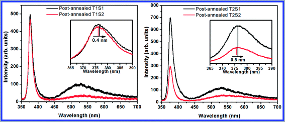
The impact of the Te levels on the optical features of the post-annealed samples (T1S1, T1S2, T2S1, and T2S2) was studied using PL spectrometry at ambient temperature, and the obtained results are demonstrated in Fig. 6. In general, two emission bands are observed in the PL spectra of ZnO. One of them is located in the UV range (sharp band), corresponding to the near band edge transition of ZnO, specifically the recombination of free excitons. The other one is in the visible region (broad band), originating from the recombining electron–holes at a deep level (DL), likely due to the oxygen and zinc vacancies, zinc and oxygen interstitials, impurities, dopants, and surface states.25–27 The UV/DL ratio is the key factor for comparing the optical features of the achieved morphologies. The larger ratio represents a better quality of crystallinity. Consequently, a better relative quality of crystallinity was obtained for the post-annealed T1S2 and T2S1 samples. The PL spectra observed for the acquired nanostructures are the same as those reported for the Te-doped ZnO nanostructures.17 Shifts less than 1 nm were observed in the achieved morphologies upon closer inspection of the UV spectra. On the other hand, shifts with greater values were observed for the films deposited in higher deposition time than for those deposited in lower time of deposition. In the visible region, it is reasonable to consider that the broad visible peak contains three narrower peaks in the green, yellow, and red emission region, originating from the diverse defect mechanisms. Diverse visible emissions associated with the existence of defects were observed for the acquired morphologies, which could be due to the diverse morphologies and dopant amounts. From the SEM, EDS, and surface analysis, it can be concluded that a better relative quality of crystallinity is achieved by combining different factors, including the morphologies and chemical compositions (oxygen deficiency and atomic percentage of Te) of the post-annealed T1S2 sample.
 |
| | Fig. 6 PL spectra of the post-annealed samples. | |
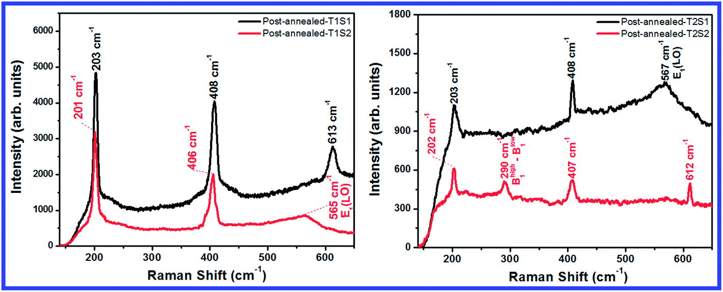
Fig. 7 shows the Raman spectra of the post-annealed samples grown on the zinc substrate. Sharp and strong peaks at 201 to 203 cm−1 in the spectra of all the samples are assigned to the resonance and can be attributed to the second order Raman spectra arising from the zone-boundary phonons.28 The weak band at 290 cm−1 for the post-annealed T2S2 sample is assigned to the Bhigh1 − Blow1 that is the salient mode of wurtzite ZnO. This band may be related to the intrinsic host lattice defects that are activated by the dopant atoms or the incorporation of impurities.29 Strong Raman bands in the range from 406 to 408 cm−1 are related to the transversal mode of ZnO.30 Broad bands at 565 and 567 cm−1 are due to the impurities and formation of defects, such as oxygen vacancies.31 The disappearance of this band from the spectrum of the post-annealed T2S2 sample indicates a better crystallinity of these samples as compared to that of the other samples, and this in good agreement with the PL results. The origin of the Raman bands at 612 and 613 cm−1 is not yet clear; however, it has been reported that these bands can be attributed to the changes due to doping.32
 |
| | Fig. 7 Raman spectra of the post-annealed samples. | |
As is well known, field electron emission is defined as the extraction of electrons from the condensed matter into a vacuum through tunneling via a surface potential barrier using a strong electric field. However, many factors can be influenced by the outcomes of field emission behavior, including the geometric properties, crystallinity (defects and impurities), and chemical parameters of the emitters, whereas testing ZnO nanowires doped with Te is significant as no report is available in this regard. Fig. 8 shows the field emission current density versus the applied field (J–E) of the Te-doped ZnO nanowires (post-annealed samples: T1S1, T1S2, T2S1, and T2S2). The turn-on field related to the emission current density of about 0.1 μA is 1.21 V μm−1 for T1S1 sample and 1.40 V μm−1 for the T1S2 sample. When higher voltage was used, the emission current quickly increased, and an emission current density of ∼350 μA cm−2 was derived from the T1S1 and T1S2 samples at the used fields of ∼3.02 V μm−1 and 3.33 V μm−1, respectively. In addition, the turn-on fields corresponding to the emission current density of 0.1 μA were found to be 2.05 V μm−1 and 3.6 V μm−1 for the post-annealed T2S1 and T2S2 samples, respectively. As the applied voltage increased, the emission current rapidly increased and the emission current densities of 115.5 μA cm−2 and 74 μA cm−2 were derived from the post-annealed T2S1 and T2S2 samples at the applied fields of 4.86 V μm−1 and 6.8 V μm−1, respectively.
In semiconducting field emitters, the current of emission consists of tunneling of the charge carriers from both conduction and valence bands.33 First, tunneling of the charge carriers from the conduction band is the main reason for the emission at a lower field strength and the current of emission can also result from the tunneling of the charge carriers from the valence band in a higher electric field. To compare our results with those reported in the literature, threshold fields of 2.13 V μm−1, 2.42 V μm−1, and 4.6 V μm−1 for the post-annealed T1S1, T1S2, and T2S1 samples are required to draw an emission current density of ∼100 μA cm−2. In the present study, the current density J is defined as J = I/A, where I refers to the determined current of emission and A represents the entire emitter area. The applied field E is described through the equation E = V/d, where V refers to the used voltage and d refers to the distance between the emitter cathode and the anode. In addition, this field is described as the “mean field”. The Fowler–Nordheim (F–N) equation was used to analyze the emission current density versus the applied field characteristics.34
| | | J = A (β2E2/φ)exp(−Bφ3/2/βE) | (12) |
where
J refers to the emission current density,
A (1.54 × 10
−6 A eV V
−2) and
B (6.83 × 10
9 eV
−3/2 V m
−1) are constants,
φ represents the work function, and
β is the enhancement factor of the field. As previously mentioned, several factors reduce the value of the turn-on field, including small tip radius, high aspect ratio, density, alignment, a smaller surface work function, and greater crystallinity. In the present study, it is expected that the hybrid impact of the aspect ratio, density of the emitters, and chemical composition should be the key parameters influencing the field emission outcomes. The T1S1 sample shows a lower turn-on field and this may be attributed to the higher aspect ratio and the presence of Te, which can contain a high field enhancement factor at the tip apex of the emitters with reduced electric field screening effects from the neighboring wires. The observed turn-on field values are superior/comparable to those reported for different ZnO nanostructures (
Table 3).
11,22,35–43
Table 3 Key performance parameters of the various field emitters (nanostructures/thin films). The turn-on field and threshold field refer to the values of the applied field required to draw the emission current densities of ∼0.1 μA cm−2 and 1 mA cm−2, respectively. If other values are used, they have been mentioned in parentheses
| Morphology |
Synthesis method |
Turn-on field (V μm−1) |
Threshold field (V μm−1) |
Field enhancement factor (β) |
Substrate |
Ref |
| Nanowires |
Electrodeposition and annealing in air |
1.2 (best result) |
2.6 (100 μA cm−2) |
— |
Zn foil |
22
|
| Nanowires |
Thermal oxidation (annealing in air) |
2.40 |
3.40 (100 μA cm−2) |
— |
Zn foil |
35
|
| Nanopins |
Vapor transport process |
1.92 |
5.90 |
657 |
Cu/Si |
36
|
| Nanorods |
Thermal evaporation process |
4.10 |
7.50 |
— |
Si |
37
|
| Nanoscrews |
Vapor phase growth |
3.60 (10 μA cm−2) |
11.20 (1.2 mA cm−2) |
— |
p-Si (100) |
38
|
| Nanobelts |
Thermal oxidation (annealing in oxygen) |
2.30 |
5.30 |
6720 |
Brass foil |
11
|
| Nanotubes |
Hydrothermal reaction |
7.00 |
17.80 |
910 |
Cu plate |
39
|
| Nanoneedles |
Solution route |
4.20 (10 μA cm−2) |
7.20 |
2350 |
Fe–Co–Ni alloy |
40
|
| Chemical route |
3.60 (10 μA cm−2) |
5.40 |
2664 |
p-Si (100) |
41
|
| Filtered cathodic vacuum arc technique |
4.10 |
9.60 |
1134 |
Polyamide foil |
42
|
| Thermal oxidation |
5.90 (2.53 mA cm−2) |
— |
4112 |
Zn/Cu |
43
|
| Thermal oxidation |
1.21 |
3.02 (350 μA cm−2) |
4659 |
T1S1 |
This work |
| 1.40 |
3.33 (350 μA cm−2) |
3701 |
T1S2 |
| 2.05 |
4.86 (115.5 μA cm−2) |
3191 |
T2S1 |
| 3.6 |
6.8 (74 μA cm−2) |
β (low electric field): 1844 β (high electric field): 2713 |
T2S2 |
The inset of Fig. 8 demonstrates the Fowler–Nordheim (F–N) plot, i.e. ln(J/E2) versus (1/E), extracted from the observed J–E characteristics. Despite the semiconducting nature of the Te-doped ZnO nanowires (post-annealed T1S1 and T1S2), the F–N plots indicate a non-linear behavior. The same feature was observed for the other samples (post-annealed T2S1 and T2S2). The field enhancement factor β is estimated using the following equation: β = (−6.8 × 10³φ3/2)/m, where φ is a work function of the emitter (φZnO = 5.3 eV) and m is the slope of the F–N plot.44 The field enhancement factors β were calculated and are listed in Table 3. Non-linear behavior is expected for the F–N plot of the semiconducting emitter, which provides I–V measurements in an adequately high field range. These non-linear F–N plots have been observed for the ZnO nanostructures.22
 |
| | Fig. 8 Field emission current density versus applied field (J–E) of the post-annealed T1S1, T1S2, T2S1, and T2S2 samples (the inset shows the corresponding Fowler–Nordheim (F–N) plots of the samples). | |
The constancies of the emission currents of ZnO nanowires doped with Te (post-annealed T1S1 and T1S2) have been studied at a preset current of 10 μA over 4 hours. Fig. 9 shows the plot of the emission current versus time (I–t) at the base pressure of 1 × 10⁻⁸ mbar. In the case of T1S1, the emission current first increased, and then it stabilized at the minimum value of ∼14 μA after 2 hours. In the case of the post-annealed T1S2 sample, the current initially fixed, and after 1 hour, it stabilized at a lower value of about 8 μA. The total current constancy was fairly good at the “fixed value”. The observed reduction in the emission current is followed by a stabilizing effect that is indicative of the “conditioning” of the total surface over continuous emission. The emission current shows excursions from the mean value along with several superimposed spike-type fluctuations and, consequently, stabilization with the decreased fluctuations. The spike-type fluctuations are due to the adsorption, desorption and/or migration of the residual gas molecules on the surface of the emitter. The changes in the emission current may be due to the bombardment of the residual gas ions during the continuous emitter operation. The findings show that the mean current of emission was fairly stable during the total period, which demonstrates an excellent physical and chemical stability of the emitter. The obtained results suggest that ZnO nanowires doped with Te may be an important system for application in the devices based on field emission. Fig. 9 shows a common field emission image obtained at a current of 10 μΑ. The image indicates several tiny spots corresponding to the emissions from the most protruding nanowires. Temporal variations in the intensity of the image spots, commensurating with the fluctuation of the emission current, were observed, as demonstrated in the I–t plots.
 |
| | Fig. 9 Field emission current stability (I–t) plots of the post-annealed samples: (a) T1S1 and (b) T1S2. The insets show typical field emission images. | |
4. Conclusions
In conclusion, a successful synthesis of the ZnO nanowire films doped with Te was carried out through electrodeposition on the zinc foil. XRD and surface analysis showed that the Te atoms substitutionally occupy the oxygen sites in the ZnO wurtzite phase. PL and Raman studies demonstrate different emission bands originating from different transition mechanisms. The field emission behavior of the Te-doped ZnO nanowire emitters have been observed to be superior than those reported for the other ZnO nanostructures in terms of turn-on and threshold field values. The semiconducting nature of the emitters was confirmed by the non-linear behavior of the F–N plots in the total range of the applied field. Superior emission current constancy was obtained for the post-annealed film with a lower concentration of wires the preset value of ∼10 μA over 4 hours. Therefore, this technique suggests a convenient way to produce ZnO wire films as high current electron sources to be applied in the field emission devices.
Acknowledgements
This work was financially supported by the Ahvaz Branch, Islamic Azad University, Ahvaz, Iran. The author is grateful to Prof. D. S. Joag and Prof. M. A. More from the Department of Physics, University of Pune, India, for their instrumentation support. The author would also like to thank Dr M. R. Mahmoudian from the University of Farhangian, Iran, for a helpful discussion.
References
- U. Özgür, Y. I. Alivov, C. Liu, A. Teke, M. A. Reshchikov, S. Doğan, V. Avrutin, S. J. Cho and H. Morkoç, J. Appl. Phys., 2005, 98, 041301 CrossRef.
- Z. Hu, D. J. Escamilla Ramírez, B. E. Heredia Cervera, G. Oskam and P. C. Searson, J. Phys. Chem. B, 2005, 109, 11209–11214 CrossRef CAS PubMed.
- J. Singh, S. S. Patil, M. A. More, D. S. Joag, R. S. Tiwari and O. N. Srivastava, Appl. Surf. Sci., 2010, 256, 6157–6163 CrossRef CAS.
- H. Yu, Z. Zhang, M. Han, X. Hao and F. Zhu, J. Am. Chem. Soc., 2005, 127, 2378–2379 CrossRef CAS PubMed.
- N. S. Ramgir, D. J. Late, A. B. Bhise, I. S. Mulla, M. A. More, D. S. Joag and V. K. Pillai, Nanotechnology, 2006, 17, 2730–2735 CrossRef CAS.
- Z. W. Pan, Z. R. Dai and Z. L. Wang, Science, 2001, 291, 1947–1949 CrossRef CAS PubMed.
- X. Y. Kong, Y. Ding, R. Yang and Z. L. Wang, Science, 2004, 303, 1348 CrossRef CAS PubMed.
- X. Y. Kong and Z. L. Wang, Nano Lett., 2003, 3, 1625–1631 CrossRef CAS.
- J. Singh, P. Kumar, D. J. Late, T. Singh, M. A. More, D. S. Joag, R. S. Tiwari, K. S. Hui and O. N. Srivastava, Dig. J. Nanomater. Biostruct., 2012, 7, 525–536 Search PubMed.
- M. Ahmad and J. Zhu, J. Mater. Chem., 2011, 21, 599–614 RSC.
- K. Huo, Y. Hu, J. Fu, X. Wang, P. K. Chu, Z. Hu and Y. Chen, J. Phys. Chem. C, 2007, 111, 5876–5881 CAS.
- J.-J. Wu and S.-C. Liu, J. Phys. Chem. B, 2002, 106, 9546–9551 CrossRef CAS.
- Y. W. Heo, V. Varadarajan, M. Kaufman, K. Kim, D. P. Norton, F. Ren and P. H. Fleming, Appl. Phys. Lett., 2002, 81, 3046 CrossRef CAS.
- R. Yousefi, F. J. Sheini, M. R. Muhamad and M. A. More, Solid State Sci., 2010, 12, 1088–1093 CrossRef CAS.
- S. Peulon and D. Lincot, Adv. Mater., 1996, 8, 166–170 CrossRef CAS.
- F. Jamali Sheini, I. S. Mulla, D. S. Joag and M. A. More, Thin Solid Films, 2009, 517, 6605–6611 CrossRef.
- F. Jamali-Sheini, R. Yousefi, M. R. Mahmoudian, N. Ali Bakr, A. Sa΄aedi and N. Ming Huang, Ceram. Int., 2014, 40, 7737–7743 CrossRef CAS.
- M. Yan, H. T. Zhang, E. J. Widjaja and R. P. H. Chang, J. Appl. Phys., 2003, 94, 5240 CrossRef CAS.
- J. Jie, G. Wang, X. Han, Q. Yu, Y. Liao, G. Li and J. G. Hou, Chem. Phys. Lett., 2004, 387, 466–470 CrossRef CAS.
- H. Chen, J. Qi, Y. Huang, Q. Liao and Y. Zhang, Acta Phys.-Chim. Sin., 2007, 23, 55–58 CrossRef CAS.
- S. Y. Li, P. Lin, C. Y. Lee, T. Y. Tseng and C. J. Huang, J. Phys. D: Appl. Phys., 2004, 37, 2274–2282 CrossRef CAS.
- F. Jamali Sheini, D. S. Joag and M. A. More, Ultramicroscopy, 2009, 109, 418–422 CrossRef CAS PubMed.
-
G. E. Muilenberg, Handbook of X-ray photoelectron spectroscopy, Perkin-Elmer Crop., 1979 Search PubMed.
- R. Yousefi, M. R. Muhamad and A. K. Zak, Thin Solid Films, 2010, 518, 5971–5977 CrossRef CAS.
- Y.-I. Kim and R. Seshadri, Inorg. Chem., 2008, 47, 8437–8443 CrossRef CAS PubMed.
- V. A. L. Roy, A. B. Djurišić, W. K. Chan, J. Gao, H. F. Lui and C. Surya, Appl. Phys. Lett., 2003, 83, 141 CrossRef CAS.
- Y.-I. Kim and R. Seshadri, Inorg. Chem., 2008, 47, 8437–8443 CrossRef CAS PubMed.
- H. Tang, L. Zhu, H. He, Z. Ye, Y. Zhang, M. Zhi, Z. Yang, B. Zhao and T. Li, J. Phys. D: Appl. Phys., 2006, 39, 2696 CrossRef CAS.
- K. Vojisavljević, M. Šćepanović, T. Srećković, M. Grujić-Brojčin, Z. Branković and G. Branković, J. Phys.: Condens. Matter, 2008, 20, 475202 CrossRef.
- S. B. Yahia, L. Znaidi, A. Kanaev and J. P. Petitet, Spectrochim. Acta, Part A, 2008, 71, 1234–1238 CrossRef PubMed.
- S. Khosravi-Gandomani, R. Yousefi, F. Jamali-Sheini and N. M. Huang, Ceram. Int., 2014, 40, 7957–7963 CrossRef CAS.
- E. Manikandan, V. Murugan, G. Kavitha, P. Babu and M. Maaza, Mater. Lett., 2014, 131, 225–228 CrossRef CAS.
- A. A. Al-Tabbakh, M. A. More, D. S. Joag, I. S. Mulla and V. K. Pillai, ACS Nano, 2010, 4, 5585–5590 CrossRef CAS PubMed.
- R. H. Fowler and L. Nordheim, Proc. R. Soc. A, 1928, 119, 173–181 CrossRef CAS.
- F. Jamali Sheini, D. S. Joag, M. A. More, J. Singh and O. N. Srivasatva, Mater. Chem. Phys., 2010, 120, 691–696 CrossRef CAS.
- C. X. Xu and X. W. Sun, Appl. Phys. Lett., 2003, 83, 3806 CrossRef CAS.
- Q. Zhao, X. Y. Xu, X. F. Song, X. Z. Zhang, D. P. Yu, C. P. Li and L. Guo, Appl. Phys. Lett., 2006, 88, 033102 CrossRef.
- L. Liao, J. C. Li, D. H. Liu, C. Liu, D. F. Wang, W. Z. Song and Q. Fu, Appl. Phys. Lett., 2005, 86, 083106 CrossRef.
- A. Wei, X. W. Sun, C. X. Xu, Z. L. Dong, M. B. Yu and W. Huang, Appl. Phys. Lett., 2006, 88, 213102 CrossRef.
- J. Liu, X. Huang, Y. Li, X. Ji, Z. Li, X. He and F. Sun, J. Phys. Chem. C, 2007, 111, 4990–4997 CAS.
- U. N. Maiti, S. F. Ahmed, M. K. Mitra and K. K. Chattopadhyay, Mater. Res. Bull., 2009, 44, 134–139 CrossRef CAS.
- H. Y. Yang, S. P. Lau, S. F. Yu, L. Huang, M. Tanemura, J. Tanaka, T. Okita and H. H. Hng, Nanotechnology, 2005, 16, 1300–1303 CrossRef CAS.
- Y. Liu, C. Pan, Y. Dai and W. Chen, Mater. Lett., 2008, 62, 2783–2786 CrossRef CAS.
- D. J. Late, P. Misra, B. N. Singh, L. M. Kukreja, D. S. Joag and M. A. More, Appl. Phys. A: Mater. Sci. Process., 2009, 95, 613–620 CrossRef CAS.
|
| This journal is © The Royal Society of Chemistry 2016 |
Click here to see how this site uses Cookies. View our privacy policy here.