The polarization-dependent anisotropic Raman response of few-layer and bulk WTe2 under different excitation wavelengths

Qingjun Songab, Haifeng Wangcd, Xiaolong Xuab, Xingchen Pancd, Yilun Wangab, Fengqi Songcd, Xiangang Wan*cd and Lun Dai*ab
aState Key Lab for Mesoscopic Physics and School of Physics, Peking University, Beijing 100871, China. E-mail: lundai@pku.edu.cn
bCollaborative Innovation Center of Quantum Matter, Beijing 100871, China
cNational Laboratory of Solid State Microstructures, College of Physics, Nanjing University, Nanjing 210093, China. E-mail: xgwan@nju.edu.cn
dCollaborative Innovation Center of Advanced Microstructures, Nanjing University, Nanjing 210093, China

Received 23rd September 2016 , Accepted 22nd October 2016

First published on 24th October 2016


Abstract

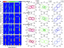
WTe2, an orthorhombic semimetal crystallized in Td phase, is a new transition metal dichalcogenide (TMD) that recently arouses great interest because of its properties of unsaturated giant magnetoresistance, Lifshitz transition and novel type II Weyl semimetal. Its covalently bonded W atoms form a zigzag W–W chain, which leads to the distinct in-plane anisotropy. In this paper, we investigate the polarization-dependent anisotropic Raman response of WTe2 with the thickness from monolayer to bulk under different excitation wavelengths, by rotating the incident laser polarization while fixing the sample and scattered polarization. The polar plots of the intensities for all detected modes exhibit two-lobed shape, while the main-axis orientations for different symmetric modes are different. These anisotropic results are first roughly fitted based on the Placzek approximated intensity, and then analyzed by the full quantum model considering the anisotropic electron–photon and anisotropic electron–phonon interactions. This work not only demonstrates the thickness and excitation wavelength dependence of the anisotropic Raman modes in WTe2, but also reveals the origin of the Raman anisotropy, which will be helpful for the research about anisotropic optical, electrical, and mechanical properties of TMDs as well as their device application.


1. Introduction

Recently, transition metal dichalcogenides (TMDs), black phosphorus and other two-dimensional (2D) materials have attracted enormous attention, because of their novel optical and electronic properties.1–15 In the TMDs family, MoS2, WS2, MoSe2 and WSe2, with the stable 2H-type phase, belong to the hexagonal crystal system, which is in-plane isotropic. ReS2 and ReSe2, with 1T′ phase, belong to the triclinic crystal system, which is in-plane anisotropic.11–14,16 WTe2 is a new family member of TMDs. Different from the triclinic semiconductor ReS2 and ReSe2 crystallized in 1T′ phase, WTe2 is an orthorhombic semimetal and crystallizes in Td phase with higher symmetry.17,18 The covalently bonded W atoms form a zigzag W–W chain, which leads to the distinct anisotropy in the two dimensional plane. The recent discoveries of non-saturating giant positive magnetoresistance, pressure driven superconductivity and temperature induced Lifshitz transition arouse great interest in this material.18–21 In addition, WTe2 is predicted to be a novel type-II Weyl semimetal.22

As a powerful optical means to investigate the lattice vibration and elementary excitations, Raman spectroscopy has been widely used in the characterization of 2D materials.23 The Raman response of an in-plane anisotropic 2D material depends subtly on the relative relations between the crystalline orientation and the polarizations of the incident laser and Raman scattered photons.12,16,24–27 So far, the anisotropic Raman responses of ReS2, ReSe2, and black phosphorus, which are largely influenced by the thickness, excitation wavelength and polarization geometry, have been thoroughly investigated,12,16,24–27 and these of other in-plane anisotropic materials deserve to be further investigated. The recent Raman research about few-layer and bulk WTe2 has focused on the signatures, frequency shift, phonon dispersion as well as the lattice vibrations.28,30 The angle-dependent Raman spectra of WTe2 have been used to identify the crystalline orientation and mode's symmetry.29 The polarization-dependent Raman spectra of few-layer and bulk WTe2 under different excitation wavelengths as well as the physical origin of the anisotropy in Raman modes need to be further explored.

In this paper, we have investigated the polarization-dependent anisotropic Raman response of WTe2 with different thicknesses under different excitation wavelengths. We first classify the detected modes into three types based on their different anisotropic Raman behaviors by rotating sample in the parallel-polarized configuration. Then we carry out the Raman measurement by rotating the incident laser polarization while fixing both the sample orientation and scattered polarization. Under this measurement method, all three types of Raman modes exhibit two-lobed shape in intensity. For modes with different symmetries, the main-axis orientations are different. In few-layer WTe2, the included angle between the main-axis orientations of two types of A′ modes changes as the excitation energy changes. The main-axis of A′′ mode is sensitive to the crystalline orientation. Their polarization-dependent intensities roughly coincide with the semi-classical model based on the Placzek approximation, except for some experimental data. Using the full quantum model based on the density functional and quantum perturbation theories, we demonstrate that the anisotropy of Raman modes is both influenced by the anisotropic electron–photon interaction and anisotropic electron–phonon interaction. Our research not only demonstrates the thickness and excitation wavelength dependence of the anisotropic Raman modes in WTe2, but also reveals the origin of the anisotropy, which may be of help in the further investigation about anisotropic optical, electrical, and mechanical properties of TMDs as well as their device application.

2. Results and discussion

The few-layer WTe2 flakes are exfoliated on 300 nm SiO2/Si substrates. Two typical optical images (Carl Zeiss Axio Imager A2m) of them are shown in Fig. 1(a). Their thicknesses are first estimated by the optical contrast and then measured by the atomic force microscope (Asylum Research). Fig. 1(b) depicts the high-resolution transmission electron microscopy (HR-TEM, Tecnai F30) image of a WTe2 flake, where the crystalline orientation can be identified by the zigzag W–W atoms chain (see more clearly in Fig. 1(c)) indicated by the white double-arrows. The fast Fourier transform (FFT) image (in the inset) depicts a distorted hexagon, which origins from the two different bond lengths between W and Te atoms. The crystal structure of monolayer WTe2 from top view and that of bilayer WTe2 from side view (i.e., the stacking patterns between neighbored layers) are shown in Fig. 1(c). We can see that, in the 2D plane, the W atoms form a zigzag chain, which is different from the connected diamond (rhombus)-shape chains in triclinic ReS2 and ReSe2. In addition, the neighbored layers stack vertically, together with the perpendicular crystalline a- and b-axis, form the orthorhombic structure. Notably, the symmetry of bulk WTe2 belongs to the space group Pnm21 and point group C72v.28,29 Its symmetry is lower than that of hexagonal 2H-type TMDs (e.g. MoS2), but higher than that of triclinic 1T′-type ones (e.g. ReS2 and ReSe2). Monolayer WTe2 belongs to the point group C22h, while N-layer (N ≥ 2) WTe2 belongs to point group C1s. In addition, the symmetry for N-layer (N ≥ 2) WTe2 has no relation with its number of layers N.29,30
image file: c6ra23687a-f1.tif
Fig. 1 (a) Two typical optical images of few-layer WTe2 flakes exfoliated on 300 nm SiO2/Si substrates. (b) The HR-TEM image of a few-layer WTe2. The crystalline a-axis is indicated by the white double-arrows. The inset is the corresponding FFT image. (c) The top-view crystal structure of monolayer WTe2, and side-view crystal structure of bulk WTe2. (d) Typical Raman spectra of mono- to nine-layer WTe2 as well as bulk WTe2 under the excitation energy of 1.96 eV. (e) The angle-dependent Raman intensity spectra of few-layer WTe2 flake, obtained by rotating the sample in the parallel-polarized configuration. (f) The zoomed-in spectra in the frequency ranges of 125–145 and 152–172 cm−1 at four representative sample rotation angles. (g), (h) and (i) The representative angle-dependent intensities of type I A′ mode (81 cm−1), type II A′ mode (165 cm−1), and A′′ mode (93 cm−1), respectively, together with their corresponding atomic displacements of lattice vibration. The main-axis in two-lobed polar plot is labeled in black double-arrows.

The typical Raman spectra of mono- to nine-layer WTe2 under the excitation energy of 1.96 eV is shown in Fig. 1(d). For multi-layer and bulk WTe2, there are about ten phonon modes detected in high-frequency (>50 cm−1) region, more than those reported in 2H-type TMD, but fewer than those reported in 1T′-type TMD.12,16,29,31 This is easy to be understood. For TMDs, under the same condition, the higher the crystal symmetry is, the less the Raman modes can be detected. With the increasing number of layers, the frequencies of some modes blue-shift while these of other ones red-shift, in accordance with previous reports.31 For simplicity, we use the frequencies of modes in bulk WTe2 to represent these of the corresponding modes in N-layer WTe2. It is worth noting that fewer modes appear in monolayer WTe2, which may be due to the absence of interlayer coupling.30

Usually, there are two non-equivalent methods to investigate the in-plane anisotropic Raman response. One is rotating the sample, while fixing the incident and scattered light polarizations.12,24–27,29,32 The other one is changing the incident laser polarization by rotating the half-wave plate while fixing both the sample orientation and scattered polarization.33 Fig. 1(e) shows the angle-dependent Raman spectra by rotating the few-layer WTe2 sample in the parallel-polarized configuration, where the incident laser polarization is parallel to the scattered light polarization. The excitation energy is 1.96 eV. For clarity, we plot the spectra in the frequency ranges of 125–145 and 152–172 cm−1 at four representative sample rotation angles in Fig. 1(f). The three modes located at ∼133, 135 and 137 cm−1 have similar angle-dependent relation, which is different from that of the two ones located at ∼163, 165 cm−1. In the range of 360°, some modes show two-lobed shape while others show four-lobed shape. This phenomenon can be understood based on the classical Placzek approximated intensity, which is proportional to |ei·[R with combining tilde]·es|2.25,34,35 The unitary vectors of incident (ei) and scattered (es) light polarization are both (cos[thin space (1/6-em)]θ sin[thin space (1/6-em)]θ 0). Here, θ is the sample rotation angle, and the initial incident laser polarization is along the crystalline a-axis. The related Raman tensors from monolayer to bulk WTe2 are summarized in Table 1. For few-layer WTe2, the intensities of A′ and A′′ modes are proportional to image file: c6ra23687a-t1.tif (two-lobed shape) and d2[thin space (1/6-em)]sin2(2θ) (four-lobed shape), respectively. We classify the detected modes into three types based on their angle-dependent behaviors. The two-lobed A′ modes include two types: type I A′ modes correspond to the main-axis in the polar plot perpendicular to the zigzag W–W chains, while type II A′ modes correspond to the main-axis parallel to the W–W chains; the four-lobed modes are A′′ modes. Three representative polar plots for these three types of modes together with their corresponding atomic displacements of lattice vibration are shown in Fig. 1(g), (h) and (i), respectively.

Table 1 The symmetry analysis and Raman tensors for monolayer, N-layer (N ≥ 2) and bulk WTe2
  1-Layer WTe2 N-Layer WTe2 (N ≥ 2) Bulk WTe2
Space group P21/m Pm Pnm21
Point group C22h C1s C72v
Irreducible representations at Г point 6Ag + 3Au + 3Bg + 6Bu 6NA′ + 12NA′′ 12A1 + 7A2 + 6B1 + 11B2
Raman tensors image file: c6ra23687a-t3.tif image file: c6ra23687a-t4.tif image file: c6ra23687a-t5.tif
image file: c6ra23687a-t6.tif image file: c6ra23687a-t7.tif image file: c6ra23687a-t8.tif
    image file: c6ra23687a-t9.tif
    image file: c6ra23687a-t10.tif


Compared with the sample rotation method, the incident polarization rotation method is more convenient and time-saving, since the half-wave plate can be electrically-driven. Therefore, this method is more suitable for the investigation of the thickness and excitation wavelength dependent Raman response. The measurement setup is shown in Fig. 2(a). Two polarizers are allocated to confirm the initial parallel relation between the incident and scattered light polarization, i.e., the initial polarization angle is 0°. Fig. 2(b) shows the Raman spectra of 1-layer, 3-layer and bulk WTe2, under the excitation energy of 1.96 eV, at four representative polarization angles (0°, 30°, 60° and 90°). The respective inset shows the corresponding measured position. Only three modes (∼81, 165, 212 cm−1) are detected in monolayer WTe2. The full width at half maximum (FWHM) for the mode located at ∼164 cm−1 is much wider than that of the corresponding mode in thicker WTe2. The polarization-dependent normalized Raman intensity spectra in the range from 0° to 360° for the three samples are shown in Fig. 2(c). All the modes in WTe2 with different thicknesses show significant in-plane anisotropy. Interestingly, all the detected modes show two-lobed shape. As discussed above, the detected modes are classified three types. We plot the polarization-dependent intensities for the three types of modes in 1-layer, 3-layer and bulk WTe2 in Fig. 2(d). We can see that for the three WTe2 samples, type I Ag (A′, A1) modes (∼81 and 212 cm−1) and type II Ag (A′, A1) mode (∼165 cm−1) exhibit similar two-lobed shape with slightly different main-axis orientations. However, the A′′ (A2) modes (∼93, 111 cm−1) exhibit distinctly different two-lobed shape for different samples. Since the θ0 (defined below) of the three samples are different, the above results show that the main-axis orientation for Ag (A′, A1) mode is not very sensitive to the crystalline orientation, while that for A′′ (A2) mode is very sensitive to the crystalline orientation.


image file: c6ra23687a-f2.tif
Fig. 2 (a) The measurement setup of the incident polarization rotation method for studying the anisotropic Raman response. (b) The Raman spectra of 1-layer, 3-layer and bulk WTe2 at four representative polarization angles of 0°, 30°, 60° and 90°. The excitation energy is 1.96 eV. The insets depict the corresponding measured positions and the initial incident polarization direction. (c) The polarization-dependent normalized Raman intensity spectra in the range from 0° to 360° for the three samples. (d) The polarization-dependent intensity polar plots, together with the curve fitting results, of the three types of modes in 1-layer, 3-layer and bulk WTe2. (e) Typical Raman spectra of few-layer (∼8-layer) WTe2 excited by four different excitation energies.

To further investigate the excitation wavelength dependence for the anisotropic Raman response, we vary the excitation laser energy and chose the few-layer WTe2 (∼8-layer) as the representative sample. In the measurement, the sample is fixed. The typical Raman spectra under four different laser excitations (1.83, 1.96, 2.28 and 2.54 eV) are shown in Fig. 2(e). Under different excitations, the relative intensities of the detected Raman modes are different. Some modes are even hard to be detected under the excitation of 2.54 eV. These demonstrate the significant excitation wavelength dependence of the Raman mode intensity in WTe2. Fig. 3(a) shows the polarization-dependent normalized Raman intensity spectra under four different excitation energies. All the detected modes show obvious polarization-dependent two lobed shape. Fig. 3(b)–(e) show the detailed polar plots for the polarization-dependent intensities of the detected modes (classified into three types, as described above) under those four excitation energies, respectively. It is interesting that the main-axis orientations for some modes are different. Under the excitation energy of 1.83 eV, there is an included angle of about 35° between the main-axis of type I A′ modes (∼81, 135 and 212 cm−1) and that of type II A′ ones (∼118 and 165 cm−1). That included angle decreases to about 30°, 10° and 0° as the excitation energy increases to 1.96, 2.28 and 2.54 eV, respectively. The main-axis orientation of A′′ modes (∼93 and 111 cm−1) remains almost unchanged as the excitation energy increases from 1.83 to 2.54 eV. To explain the above excitation wavelength dependent anisotropic experimental results, we carry out a quantitative analysis based on the semi-classical model.25,26,35 The initial incident and scattered polarization unitary vectors can both be written as (cos[thin space (1/6-em)]θ0, sin[thin space (1/6-em)]θ0, 0). Here, θ0 is the initial included angle between the incident polarization and the crystalline a-axis. As the half-wave plate is rotated with an angle of θ/2, the incident polarization rotates an angle of θ, the incident unitary vector changes to (cos(θ0 + θ), sin(θ0 + θ), 0), while the scattered one keeps constant. The intensity of a mode can be written as:

 
I ∝ |(cos(θ0 + θ), sin(θ0 + θ), 0)·[R with combining tilde]·(cos[thin space (1/6-em)]θ0, sin[thin space (1/6-em)]θ0, 0)|2 (1)
substituting it with the corresponding Raman tensors, the intensity of an Ag (A′, A1) phonon mode is:
 
IAg(A′,A1) ∝ |a[thin space (1/6-em)]cos(θ + θ0)cos[thin space (1/6-em)]θ0 + b[thin space (1/6-em)]sin(θ + θ0)sin[thin space (1/6-em)]θ0|2 (2)
and the intensity of an A′′ (A2) phonon mode is:
 
IA′′(A2) ∝ |e[thin space (1/6-em)]sin(θ + θ0)cos[thin space (1/6-em)]θ0 + e[thin space (1/6-em)]cos(θ + θ0)sin[thin space (1/6-em)]θ0|2 = |e[thin space (1/6-em)]sin(θ + 2θ0)|2 (3)
we can see that intensity variation periods for all these modes are 180°. Based on eqn (2) and (3), the maximum intensity orientation θmax for an Ag (A′, A1) phonon mode should meet the below equations:
 
(b2[thin space (1/6-em)]sin2[thin space (1/6-em)]θ0a2[thin space (1/6-em)]cos2[thin space (1/6-em)]θ0)sin[2(θmax + θ0)] + ab[thin space (1/6-em)]cos[2(θmax + θ0)]sin[thin space (1/6-em)]2θ0 = 0 (4)
and
 
(b2[thin space (1/6-em)]sin2[thin space (1/6-em)]θ0a2[thin space (1/6-em)]cos2[thin space (1/6-em)]θ0)cos[2(θmax + θ0)] − ab[thin space (1/6-em)]sin[2(θmax + θ0)]sin[thin space (1/6-em)]2θ0 < 0 (5)
similarly, the maximum intensity orientation for an A′′ (A2) mode should meet:
 
2θ0 + θmax = ±90° (6)
then, theoretically, the main-axis orientation for A′′ (A2) mode is determined by the crystalline orientation θ0, while that for Ag (A′, A1) mode is influenced by both the crystalline orientation θ0 and the Raman tensor elements (a and b), which includes real and imaginary parts, and the imaginary part is related to the absorption.26 As shown in Fig. 2(d) and 3(b)–(e), the anisotropic data can be roughly fitted by the semi-classical intensity eqn (2) and (3). The excitation wavelength dependence of the main-axis orientation of Ag (A′, A1) mode results from the different values of the Raman tensor elements a and b in eqn (4) and (5). The similar main-axis orientation of A′′ (A2) mode under different excitation energies can be understood based on eqn (6), and this feature is helpful for the identification of the crystalline orientation. Notably, some experiment data cannot be well fitted by the eqn (2) and (3), e.g., the minimum intensities of some modes are not close to zero.


image file: c6ra23687a-f3.tif
Fig. 3 (a) The polarization-dependence of the normalized Raman intensity spectra for the few-layer (∼8-layer) WTe2 flake under four different excitation energies. (b–e) The polar plots for the polarization-dependent intensities of the three types of detected phonon modes under the four excitation energies, respectively. The sample orientation is identical in these measurements.

To further explain the unfitted experimental data and explore the origin of these anisotropic Raman results, we employ the full quantum model based on the density functional theory and quantum perturbation theory for in-depth analysis.36,37 The Raman scattering response contains three processes: incident photon absorption, electron–phonon interaction, and scattered photon emission. For a certain phonon mode, the corresponding interactions in these three processes can be represented by 〈f|He–p|m1〉, 〈m1|He–ph|m2〉 and 〈m2|He–p|i〉, respectively. Here, |i〉, |m1〉, |m2〉, |f〉, He–p and He–ph are the initial state, two intermediate states, final state, electron–photon Hamiltonian and electron–phonon Hamiltonian, respectively. The laser photon energy (Elas) dependent Raman intensity can be expressed as25,26

 
image file: c6ra23687a-t2.tif(7)
where the initial electronic state |i〉 is equal to the final electronic state |f〉, ΔEmi = EmEi; Ei, Em1 and Em2 are the energies of the initial state |i〉 and intermediate states |m1〉 and |m2〉, respectively, and γ is a broadening factor related to the electron lifetimes at the intermediate state.

The incident photon absorption process contains the absorption of the photons and the transition of excited electron from the valence band to the conductance band at the Brillouin zone center Γ point. As shown in Table 1, there are three types of crystal symmetries from monolayer to bulk WTe2. For simplicity, we use the energy band structure of bilayer WTe2 to represent those of N-layer WTe2, since the crystal symmetries are same for N-layer (N ≥ 2) WTe2. The density functional theoretical (DFT) calculated band structures of monolayer, bilayer and bulk WTe2 are shown in Fig. 4(a)–(c), and the representative band symmetries at Γ point are also labelled. The electron transition from the valence band to the conductance band should satisfy the symmetry selection rules, as summarized in ESI (Table S1 and S2). Then we focus on the polarization-dependent optical absorption under certain excitation energy. We take monolayer WTe2 as an example. When the initial incident polarization and scattered polarization are along the a-axis (θ0 = 0°), for Elas ≈ 1.5 eV, the excited electron will transit from the Bu valence band to Ag conductance band according to the symmetry selection rule. The polar plot of the optical transition probability with an incident polarization angle of θ is shown in Fig. 4(d), where the maximum (minimum) absorption corresponds to the parallel (perpendicular) relation between the incident polarization and a-axis. For Elas ≈ 2.3 eV, the excited electron will transit from the Bg valence band to Au conductance band, and the corresponding polar plot is shown in Fig. 4(e), where the maximum (minimum) absorption corresponds to the perpendicular (parallel) relation between the incident polarization and a-axis. Similarly, polarization-dependent transitions from A′ (A2) valence band to A′ (B2) conductance band and from A′ (A2) valence band to A′′ (B1) conductance band can occur in multilayer (bulk) WTe2 under appropriate excitation energies, as shown in Fig. 4(b) and (c). The photon emission process can be taken as the reverse process of the above absorption process. Since the scattered polarization is fixed, then photon emission process has no influence on the polarization dependence of Raman intensity.


image file: c6ra23687a-f4.tif
Fig. 4 (a–c) The calculated band structures of monolayer, bilayer and bulk WTe2, respectively. The representative band symmetries at Γ point are labelled, and the insets are their 2D Brillouin zones. Calculated polarization dependence of the optical transition probability (d) from the Bg to Au (Elas ≈ 1.5 eV) and (e) from the Ag to Au (Elas ≈ 2.3 eV) in monolayer WTe2, as indicated in (a). 0° corresponds to the W–W chain (a-axis) direction, the initial incident polarization and scattered polarization are along the a-axis (θ0 = 0°). (f) The representative calculated polarization dependent intensities of Ag and Bg modes in monolayer WTe2 with certain θ0 (∼15°).

To study the influence of electron–phonon interaction on the anisotropic Raman scattering, we first assume the electron–phonon interaction (He–p) in the Raman scattering is not polarization dependent. In this case, the intensity of a phonon mode can be derived from the product of two anisotropic electron–photon interaction processes. Here we use the notation ab to describe a Raman measurement with the incident polarization along the W–W chains (a-axis) and scattered polarization perpendicular to the W–W chains (b-axis), and other polarization conditions aa, bb, ba are defined accordingly. For monolayer (multi-layer, bulk) WTe2, we can excite the Ag (A′, A1) modes with the aa- and bb- polarizations, and Bg (A′′, A2) modes with the ab and ba polarization conditions. For our rotating incident light polarization method, the sample and the scattered light polarization are fixed. As defined above, with the included angle θ0 between the a-axis and the scattered polarization, the unitary vector for the scattered polarization can be expressed as (cos[thin space (1/6-em)]θ0, sin[thin space (1/6-em)]θ0, 0). With the rotation angle of θ for the incident polarization, its unitary vector can be expressed as (cos(θ0 + θ), sin(θ0 + θ), 0). In this case, the representative calculated polarization-dependence for the intensities of Ag and Bg modes in monolayer WTe2 with certain θ0 (∼15°) are shown in Fig. 4(f). Obviously, they do not completely consist with all the anisotropic experimental results, especially for the modes whose minimum intensities are not close to zero, as shown in Fig. 2(d) and 3(b)–(d). For those modes, the assumption that the electron–phonon interaction in the Raman scattering is not polarization dependent is invalid. In other words, our experimental results reveal the existence of the anisotropic electron–phonon interaction in WTe2. Since electron–phonon interaction is closely related to the thermal, electrical, thermoelectric, and superconductive properties in materials,25 the anisotropic electron–phonon interaction in WTe2 may inspire the further research about the anisotropic physical property and device application.

3. Experimental

3.1 Single crystal growth of WTe2 and sample preparation

The chemical vapor transport method was used for the growth of WTe2 single crystals.19 Stoichiometric tungsten and tellurium powers were weighed and ground together in a glove box. Then the mixture was loaded into a quartz tube, and the tube was placed in a two-zone furnace. With a small amount of TeBr4 as the transport agent, the tube was sealed under vacuum. The temperatures of the two zones were maintained at 800 °C and 700 °C, respectively. The mixture was initially heated at the zone with higher temperature. After 10 days' growth, the single crystal appeared in the zone with lower temperature.

3.2 Raman measurements

The polarization-dependent Raman measurement was carried out by using a commercial micro-Raman system (Horiba Jobin Yvon HR800) under the backscattering geometry. To guarantee the high resolution of the Raman measurement, we used a 100× object lens, a grating with 1800 grooves per mm, and an exposure time of 60 seconds. The excitation laser power was controlled below 400 μW to avoid the damage to sample. In the incident light polarization rotation method, a polarizer was used to set the polarization of incident laser, and a half-wave plate was used to vary the incident polarization. The other polarizer was placed before the spectrometer. All the measurements were carried out at room temperature.

3.3 Density functional theory (DFT) calculations

The DFT calculations were carried out with the Vienna Ab initio Simulation Package (VASP) based on density functional theory.38 The Perdew–Burke–Ernzerhof (PBE) exchange-correlation functional along with the projector-augmented wave (PAW) potentials was employed for the self-consistent total energy calculations and geometry optimization.39 The kinetic energy cutoff for the plane wave basis set was chosen to be 500 eV for all calculations. The Brillouin zone were sampled using 7 × 14 × 3 (for bulk WTe2) and 7 × 14 × 1 (for 1L–3L WTe2) Monkhorst–Pack k-point grid. Atomic positions were relaxed until the energy differences were converged within 10−5 eV and the maximum Hellmann-–Feynman force on any atom was below 0.01 eV Å−1. We used a periodic supercell to simulate a 2D sheet, including vacuum of 15 Å, to separate the adjacent periodic images of the sheet. The spin–orbit interaction (SOC) was included in the calculation of electronic structures of bulk and few-layer WTe2. The van der Waals (vdW) interactions were considered at the vdW-DF40,41 level for geometry optimization, which was found to be more accurate in describing the structural properties of layered materials.

4. Conclusions

We investigate the anisotropic Raman response of WTe2 with the thickness from monolayer to bulk under different excitation energies by rotating the incident laser polarization. Prior to it, we identify the symmetry of the detected modes and classify them into three types based on their anisotropic behaviors measured by rotating the sample in the parallel-polarized configuration. Under the measurement method of rotating the incident laser polarization, all the detected Raman modes exhibit two-lobed shapes in intensity. The main-axis orientation of the two-lobed shape exhibits different excitation wavelength dependence for modes with different symmetries. We further analyze the origin of the anisotropy based on the full quantum model, which contains both the electron–photon and electron–phonon interactions. The results demonstrate that the anisotropy of Raman modes origins from the anisotropic electron–photon interaction and the anisotropic electron–phonon interaction. In addition, we also provide a useful tool to identify the crystalline orientation, which may be of help in the further investigation about anisotropic optical, electrical, and mechanical properties of TMDs as well as their device application.

Acknowledgements

We acknowledge support from the National Key Projects for Basic Research Program of China (2013CB921901, 2012CB932703, 2013CB922103, and 2011CB922103), the National Natural Science Foundation of China (Grants nos. 61521004, 61125402, 51172004, 11474007, 11225421, 11434010, 11474277, 91421109, 11134005, 61176088, 11522432, 11525417 and 11274003).

Notes and references

  1. K. F. Mak, K. He, J. Shan and T. F. Heinz, Nat. Nanotechnol., 2012, 7, 494–498 CrossRef CAS PubMed.
  2. H. Zeng, J. Dai, W. Yao, D. Xiao and X. Cui, Nat. Nanotechnol., 2012, 7, 490–493 CrossRef CAS PubMed.
  3. T. Cao, G. Wang, W. Han, H. Ye, C. Zhu, J. Shi, Q. Niu, P. Tan, E. Wang, B. Liu and J. Feng, Nat. Commun., 2012, 3, 887 CrossRef PubMed.
  4. K. F. Mak, K. L. MeGill, J. Park and P. L. McEuen, Science, 2014, 344, 1489–1492 CrossRef CAS PubMed.
  5. L. Li, Y. Yu, G. J. Ye, Q. Ge, X. Ou, H. Wu, D. Feng, X. H. Chen and Y. Zhang, Nat. Nanotechnol., 2014, 9, 372–377 CrossRef CAS PubMed.
  6. L. Li, G. J. Ye, V. Tran, R. Fei, G. Chen, H. Wang, J. Wang, K. Watanabe, T. Taniguchi, L. Yang, X. H. Chen and Y. Zhang, Nat. Nanotechnol., 2015, 10, 608–613 CrossRef CAS PubMed.
  7. L. Li, F. Yang, G. J. Ye, Z. Zhang, Z. Zhu, W. Lou, X. Zhou, L. Li, K. Watanabe, T. Taniguchi, K. Chang, Y. Wang, X. H. Chen and Y. Zhang, Nat. Nanotechnol., 2016, 11, 593–597 CrossRef CAS PubMed.
  8. J. Qiao, X. Kong, Z. X. Hu, F. Yang and W. Ji, Nat. Commun., 2014, 5, 4475 CAS.
  9. F. Xia, H. Wang and Y. Jia, Nat. Commun., 2014, 5, 4458 CAS.
  10. Z. Luo, J. Maassen, Y. Deng, Y. Du, R. P. Garrelts, M. S. Lundstrom, P. D. Ye and X. Xu, Nat. Commun., 2015, 6, 8572 CrossRef CAS PubMed.
  11. Y. C. Lin, H. P. Komsa, C.-H. Yeh, T. Björkman, Z. Y. Liang, C.-H. Ho, Y.-S. Huang, P.-W. Chiu, A. V. Krasheninnikov and K. Suenaga, ACS Nano, 2015, 9, 11249–11257 CrossRef CAS PubMed.
  12. D. A. Chenet, O. B. Aslan, P. Y. Huang, C. Fan, A. M. van der Zande, T. F. Heinz and J. C. Hone, Nano Lett., 2015, 15, 5667–5672 CrossRef CAS PubMed.
  13. E. Liu, Y. Fu, Y. Wang, Y. Feng, H. Liu, X. Wan, W. Zhou, B. Wang, L. Shao, C. H. Ho, Y. S. Huang, Z. Cao, L. Wang, A. Li, J. Zeng, F. Song, X. Wang, Y. Shi, H. Yuan, H. Y. Hwang, Y. Cui, F. Miao and D. Xing, Nat. Commun., 2015, 6, 6991 CrossRef CAS PubMed.
  14. O. B. Aslan, D. A. Chenet, A. M. van der Zande, J. C. Hone and T. F. Heinz, ACS Photonics, 2016, 3, 96–101 CrossRef CAS.
  15. Q. J. Song, Q. H. Tan, X. Zhang, J. B. Wu, B. W. Sheng, Y. Wan, X. Q. Wang, L. Dai and P. H. Tan, Phys. Rev. B: Condens. Matter Mater. Phys., 2016, 93, 115409 CrossRef.
  16. S. C. Daniel Wolverson, A. S. Kazemi, A. Ilie and S. J. Bending, ACS Nano, 2014, 8, 11154–11164 CrossRef PubMed.
  17. V. E. J. Augustin, Th. Böker, W. Frentrup, H. Dwelk, C. Janowitz and R. Manzke, Phys. Rev. B: Condens. Matter Mater. Phys., 2000, 62, 10812–10823 CrossRef.
  18. M. N. Ali, J. Xiong, S. Flynn, J. Tao, Q. D. Gibson, L. M. Schoop, T. Liang, N. Haldolaarachchige, M. Hirschberger, N. P. Ong and R. J. Cava, Nature, 2014, 514, 205–208 CAS.
  19. X. C. Pan, X. Chen, H. Liu, Y. Feng, Z. Wei, Y. Zhou, Z. Chi, L. Pi, F. Yen, F. Song, X. Wan, Z. Yang, B. Wang, G. Wang and Y. Zhang, Nat. Commun., 2015, 6, 7805 CrossRef PubMed.
  20. P. L. Cai, J. Hu, L. P. He, J. Pan, X. C. Hong, Z. Zhang, J. Zhang, J. Wei, Z. Q. Mao and S. Y. Li, Phys. Rev. Lett., 2015, 115, 057202 CrossRef CAS PubMed.
  21. Y. Wu, N. H. Jo, M. Ochi, L. Huang, D. Mou, S. L. Bud'ko, P. C. Canfield, N. Trivedi, R. Arita and A. Kaminski, Phys. Rev. Lett., 2015, 115, 166602 CrossRef PubMed.
  22. A. A. Soluyanov, D. Gresch, Z. Wang, Q. Wu, M. Troyer, X. Dai and B. A. Bernevig, Nature, 2015, 527, 495–498 CrossRef CAS PubMed.
  23. X. Zhang, X. F. Qiao, W. Shi, J. B. Wu, D. S. Jiang and P. H. Tan, Chem. Soc. Rev., 2015, 44, 2757–2785 RSC.
  24. R. He, J. A. Yan, Z. Yin, Z. Ye, G. Ye, J. Cheng, J. Li and C. H. Lui, Nano Lett., 2016, 16, 1404–1409 CrossRef CAS PubMed.
  25. X. Ling, S. Huang, E. H. Hasdeo, L. Liang, W. M. Parkin, Y. Tatsumi, A. R. Nugraha, A. A. Puretzky, P. M. Das, B. G. Sumpter, D. B. Geohegan, J. Kong, R. Saito, M. Drndic, V. Meunier and M. S. Dresselhaus, Nano Lett., 2016, 16, 2260–2267 CrossRef CAS PubMed.
  26. H. B. Ribeiro, M. A. Pimenta, C. J. S. de Matos, R. L. Moreira, A. S. Rodin, J. D. Zapata, E. A. T. de Souza and A. H. Castro Neto, ACS Nano, 2015, 9, 4270–4276 CrossRef CAS PubMed.
  27. E. Lorchat, G. Froehlicher and S. Berciaud, ACS Nano, 2016, 10, 2752–2760 CrossRef CAS PubMed.
  28. Y. C. Jiang, J. Gao and L. Wang, Sci. Rep., 2016, 6, 19624 CrossRef CAS PubMed.
  29. Q. Song, X. Pan, H. Wang, K. Zhang, Q. Tan, P. Li, Y. Wan, Y. Wang, X. Xu, M. Lin, X. Wan, F. Song and L. Dai, Sci. Rep., 2016, 6, 29254 CrossRef PubMed.
  30. J. Kim, J. U. Lee, J. Lee, H. J. Park, Z. Lee, C. Lee and H. Cheong, Nanoscale, 2015, 7, 18708–18715 RSC.
  31. J. Lee, F. Ye, Z. Wang, R. Yang, J. Hu, Z. Mao, J. Wei and P. X. Feng, Nanoscale, 2016, 8, 7854–7860 RSC.
  32. J. Wu, N. Mao, L. Xie, H. Xu and J. Zhang, Angew. Chem., 2015, 54, 2366–2369 CrossRef CAS PubMed.
  33. S. Zhang, J. Yang, R. Xu, F. Wang, W. Li, M. Ghufran, Y.-W. Zhang, Z. Yu, G. Zhang, Q. Qin and Y. Lu, ACS Nano, 2014, 8, 9590–9596 CrossRef CAS PubMed.
  34. R. Loudon, Adv. Phys., 1964, 13, 423–482 CrossRef CAS.
  35. A. C. Albrecht, J. Chem. Phys., 1961, 34, 1476 CrossRef CAS.
  36. R. Loudon, Proc. R. Soc. London, Ser. A, 1963, 275, 218–232 CrossRef CAS.
  37. W. L. Peticolas, J. Chem. Phys., 1970, 52, 1576 CrossRef CAS.
  38. G. Kresse and J. Furthmüller, Phys. Rev. B, 1996, 54, 11169–11186 CrossRef CAS.
  39. K. B. John, P. Perdew and M. Ernzerhof, Phys. Rev. Lett., 1996, 77, 3865–3868 CrossRef PubMed.
  40. M. Dion, H. Rydberg, E. Schroder, D. C. Langreth and B. I. Lundqvist, Phys. Rev. Lett., 2004, 92, 246401 CrossRef CAS PubMed.
  41. K. Lee, É. D. Murray, L. Kong, B. I. Lundqvist and D. C. Langreth, Phys. Rev. B: Condens. Matter Mater. Phys., 2010, 82, 11169–11186 Search PubMed.

Footnote

Electronic supplementary information (ESI) available. See DOI: 10.1039/c6ra23687a

This journal is © The Royal Society of Chemistry 2016
Click here to see how this site uses Cookies. View our privacy policy here.