H. T. Hsueh*a,
L. T. Laib,
Y. M. Juanc,
S. W. Huangb,
T. C. Cheng*b and
Y. D. Lina
aNational Nano Device Laboratories, National Applied Research Laboratories, Tainan 741, Taiwan. E-mail: hanting.hsueh@gmail.com
bDepartment of Mechanical Engineering, National Kaohsiung University of Applied Science, Kaohsiung 807, Taiwan. E-mail: tcchengme@kuas.edu.tw
cInstitute of Microelectronics, Department of Electrical Engineering, National Cheng Kung University, Tainan 701, Taiwan
First published on 3rd October 2016
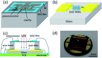
Microelectromechanical system (MEMS) piezoresistive pressure sensor and ZnO nanowires (NWs) ultraviolet (UV) photodetector were 3D integrated into a single chip with a vertically stacked structure. The MEMS pressure sensor with a UV transparent SiO2 diaphragm was stacked on the top of UV photodetector. The fabricated pressure sensor presents good linearity and stability with increasing applied pressure from 0–500 mbar. The measured interval of 0.2 mbar also shows its high sensitivity with a small change in pressure and altitude. For the ZnO NWs UV photodetector, the cutoff wavelength was around 360 nm, and the measured responsivity was 6.2 × 10⁻¹ A W−1 with 5 V applied bias. To discuss the influence of the applied pressure and UV on this 3D stacked device, the pressure sensor was also measured with and without UV illumination, and the UV photodetector was measured at various applied pressures. The results show that UV variation can be ignored for pressure sensor measurement. However, the photoresponses of ZnO NWs decreased, whereas the applied pressure was increased.
For UV photodetector, 1-D NWs-based devices have attracted considerable attention because they could provide a much larger surface-to-volume ratio compared to bulk- and film-based devices. With this advantage, NWs-based sensors normally exhibit a larger response, particularly for semiconducting metal oxide sensors. It has been reported that SnO2,3 TiO2,4 WO3 (ref. 5) and In2O3 (ref. 6) NWs can all be used as photodetectors and gas sensors. Among these metal oxides, ZnO is a thermally stable n-type semiconductor with a large exciton binding energy of 60 meV and a large bandgap energy of 3.37 eV at room temperature.7
Electronic products have changed and improved quickly in this period, particularly for consumer electronics or wearable products. The properties of light, compact and small are the trends for future products, and thus, how to reduce the product size and increase its functionalities are important issues in the current stage. Sensors with different properties are usually packaged separately. The packaging efficiency can be improved further if 3D packages can be made practical. In this experiment, a MEMS pressure sensor was vertically stacked on a UV photodetector into a single chip, which performs multi-functionalities of atmospheric pressure and UV. A SiO2 film was utilized as the diaphragm of upper pressure sensor, which allowed the UV light to pass through the pressure sensor and reach the lower UV photodetector. This unique structure allows these two different sensors to be 3D integrated vertically into one chip, which is potentially useful indoors/outdoors for wearable devices, such as smartphones or smartwatches in future.
![]() | ||
| Fig. 1 Schematic diagram of (a) pressure sensor, (b) ZnO NWs UV photodetector, and (c and d) the 3D stacked structure. | ||
The crystallographic properties and surface morphology of the as-synthesized ZnO NWs were examined by X-ray diffraction (XRD, MAC MXP18) and field-emission scanning electron microscopy (FE-SEM, JEOL JSM-7001F). While measuring, the integrated chip was placed in a sealed chamber with a transparent lid. For the pressure measurement, air with different pressures was applied to the chamber. Different deformations of the piezoresistive film cause different output voltages of the Wheatstone quarter-bridge. For UV measurement, the spectral responsivity was performed using a JOBIN-YVON SPEX system with a 300 W xenon lamp as the light source and a standard synchronous detection scheme.
![]() | ||
| Fig. 2 (a) Structural layout of piezoresistive pressure sensor. (b) Measurement of pressure sensors with different L/W ratios. | ||
![]() | ||
| Fig. 3 (a) Pressure measurements of L/W 15 pressure sensor with repeatable performance. (b) Dynamic responses measured by L/W 15 pressure sensor at 0–150 mbar. | ||
To benefit the use as an altimeter, pressure sensor with high sensitivity is important if it is used to determine the small changes in altitude. Generally, 10 mbar change in atmospheric pressure leads to around 86.2 m change in altitude. Fig. 4 shows the measurement with the interval of 0.2 mbar, which means that the pressure sensor has a resolution of 1.7 m in altitude.
For a UV photodetector, Fig. 5a shows the top view SEM image of the surface morphology after growing ZnO NWs. It can be observed clearly that high-density ZnO NWs with uniform length and diameter were grown on the substrate. Fig. 5b shows the SEM image of cross-sectional ZnO NWs, where the average length of ZnO NWs was around 1.2 μm. The inset in Fig. 5b also shows XRD analysis of these ZnO NWs. It can be observed clearly that only ZnO (002) diffraction peak appears in the whole spectrum. Such a result indicates that these ZnO NWs were oriented preferentially in the (002) direction. The full-width-half-maximum (FWHM) of the XRD θ-scan peak was only 0.16°. Such a narrow line width implies that the c-axes of these NWs are well aligned along the growth direction.
![]() | ||
| Fig. 5 (a) Top-view and (b) cross-sectional SEM images of ZnO NWs. The inset in (b) shows XRD analysis of the as grown ZnO NWs. | ||
Fig. 6a shows the responsivity of the fabricated ZnO NWs UV photodetector under a normal temperature and pressure environment (NTP, 25 °C, 1 atm) with different applied bias (1–5 V). The photoresponses of the fabricated photodetector were flat in the short wavelength region and had a sharp cutoff at around 360 nm. With an incident light wavelength of 360 nm and an applied bias of 1 V, the measured responsivity of the photodetector was 7.2 × 10⁻² A W−1. As the applied bias was increased to 5 V, the measured responsivity increased to 6.2 × 10⁻¹ A W−1. The significant increase in responsivity with the applied bias implies that there exists a photoconductive gain in the photodetector. The quantum efficiency of the UV photodetector was determined from the measured spectra response to be8,9
![]() | (1) |
![]() | ||
| Fig. 6 (a) Spectral responsivity of ZnO NWs with various applied biases. (b) Time-dependent photoresponse of ZnO NWs with UV switched on/off under NTP environment (UV: 360 nm, 1.9 mW cm−2). | ||
The photoconduction of ZnO NWs is governed mainly by the adsorption and desorption of oxygen.10 Oxygen molecules are adsorbed on the ZnO NWs surface by capturing free electrons from the metal oxide, creating a low-conductivity depletion layer near the surface of the ZnO NWs [O2(gas) + e− → O2−(ads.)]. Upon UV illumination, the photogenerated holes migrate to the surface and discharge the adsorbed oxygen ions [O2−(ads.) + h+ → O2(gas)]. This phenomenon decreases the width of the depletion region and increases the conductivity of the n-type material. These oxygen-related hole-trap states on the NWs surface can prevent charge-carrier recombination and prolong the photocarrier lifetime. Therefore, high internal photoconductivity gain can be achieved in ZnO NWs devices.9 To understand the UV-to-visible rejection ratio, this ratio was defined as the responsivity measured at 350 nm divided by the responsivity measured at 450 nm. With such a relation, we achieved a UV-to-visible rejection ratio of 57, while 5 V bias was applied.
Fig. 6b shows the transient response of the fabricated ZnO photodetector when 360 nm UV excitation was switched on and off, in intervals of 120 s. The measured current increased rapidly when the UV light was turned on and decreased sharply when the UV light was turned off. It has been reported that the rise and decay time of an n-type metal oxide is associated with the adsorption and desorption of oxygen.11–13 To discuss the response time of the photodetector, the curve in Fig. 6b was fitted by the following equation:14,15
| I = I0 + Ae−t/τ1 + Be−t/τ2 | (2) |
To improve the practicability of such vertical stacking sensors, the effects of the applied pressure and UV illumination should be discussed. Therefore, the influence of UV illumination on the pressure sensor and the influences of pressure on the photodetector were measured. After packaging these two sensors, the pressure sensor was stacked on the photodetector. Fig. 7 shows the measured results of the upper pressure sensor under different light illuminations. In a dark environment, the dynamitic responses presented stable and reproducible performance for different applied pressures 50, 100, 200 and 300 mbar. Under 245 nm and 360 nm UV light illumination, it can also be observed that the responses did not change, which almost correspond to the results in the dark environment. In this experiment, the piezoresistors were designed symmetrically and the resistance of each piezoresistor was equivalent (i.e. Ra = Rb = Rc = Rd). While pressure is applied to the diaphragm, Ra and Rc decrease due to the wider deformation, and Rb and Rd increase due to the longer deformation. The resistance under applied pressure can be expressed as follows:19
![]() | (3) |
![]() | (4) |
ZnO with a wurtzite structure in the hexagonal crystal system is symmetric and has no center of symmetry. Such a structure has favorable piezoelectric properties. Kuo et al. measured the piezoelectric properties by atomic force microscopy (AFM) on bending the ZnO NWs; the longer ZnO NWs generated larger piezoelectric current.20 Wang et al. used the AFM probe to apply stress to ZnO NWs, which made them produce strain, forming a piezoelectric nanogenerator.21 However, in this experiment, ZnO NWs were only measured under different atmospheric pressure without any bend in its morphology. Therefore, the piezoelectric effect can be ignored in this experiment when different atmospheric pressures were applied. To further understand the influence of pressure on the ZnO NWs photodetector, the I–V relationships under different applied pressures were examined. Fig. 8 shows the I–V relationships with different applied pressures in the dark environment. At 5 V bias, the current without an applied pressure was 3.09 μA, and the current increased to 2.23 μA under 300 mbar pressure, respectively. This suggests that the resistance of ZnO NWs becomes larger while the pressure increases. When pressure was applied to the diaphragm, the diaphragm deformed downward and the volume of pressure sensor's cavity changed. With increasing pressure, the increasing downward deformation of diaphragm compressed the cavity space, causing an increase in the air pressure in sensor's cavity. At 300 mbar applied pressure, more oxygen molecules are adsorbed on ZnO NWs surface due to the higher air pressure in the cavity. Therefore, more free electrons from the metal oxide were captured, forming a thicker depletion layer near the surface of the ZnO NWs and decreasing the conductivity. According to these results, higher air pressure will cause more adsorption of oxygen, which appears to possess a higher photoresponse because it has more oxygen to be released. However, in Fig. 9, the photoresponses measured under 360 nm UV illumination showed opposite results. Fig. 9b shows the enlarged diagram of the photoresponse with different applied pressures. The change in response was very small; however, it decreased when the pressure was increased. The photoresponse is related to the dark current (Id) and photo current (Ip). In this experiment, the difference of Id is small, and thus, it much relies on Ip. Li et al. reported that the photogenerated hole migrates to the surface and the trapped oxygen, forming oxygen molecule, physisorbs on the surface under UV illumination.22 The physisorbed oxygen molecule can leave the NWs surface by thermal activation at room temperature. The ability of physisorption with oxygen was restricted by the increasing ambient pressure. While the trapped oxygen was reduced by the UV generated hole, the high air pressure formed an obstructive force to prevent the physisorption of oxygen gas (Fig. 10). A part of the physisorbed oxygen on the surface may change to chemisorbed oxygen by capturing electrons from the conduction band of ZnO NWs, thereby reducing the response.22 The photoresponses in Fig. 9b also correspond to the results in which the responded currents measured at 0, 50, 100, 200 and 300 mbar were around 13, 12.8, 12.5, 12.2 and 11.9 μA, respectively.
![]() | ||
| Fig. 9 (a) Transient responses of ZnO NWs measured under different pressures with 360 nm and 1.9 mW cm−2 UV light, and (b) the enlarged diagram of (a). | ||
![]() | ||
| Fig. 10 Schematics of oxygen molecules on the surface of ZnO NWs at (a) low and (b) high pressure in the dark and under UV illumination. | ||
| This journal is © The Royal Society of Chemistry 2016 |