Few molecule SERS detection using nanolens based plasmonic nanostructure: application to point mutation detection

Gobind Das*a, Salma Alrasheeda, Maria Laura Colucciob, Francesco Gentilebc, Annalisa Nicastrid, Patrizio Candelorob, Giovanni Cudad, Gerardo Perozziellob and Enzo Di Fabrizioa
aPhysical Sciences and Engineering (PSE), King Abdullah University of Science and Technology (KAUST), Thuwal 23955-6900, Kingdom of Saudi Arabia. E-mail: gobind.das@kaust.edu.sa
bBio-Nanotechnology and Engineering for Medicine (BIONEM), Department of Experimental and Clinical Medicine, University of Magna Graecia Viale Europa, Germaneto, Catanzaro 88100, Italy
cDepartment of Electrical Engineering and Information Technology, University of Napoli, Federico II – Corso Umberto I 40, 80138 Napoli, Italy
dAdvanced Research Center on Biochemistry and Molecular Biology, Department of Experimental and Clinical Medicine, University of Magna Graecia Viale Europa, Germaneto, Catanzaro 88100, Italy

Received 19th September 2016 , Accepted 23rd October 2016

First published on 27th October 2016


Abstract

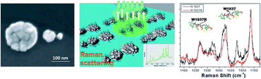
Advancements in nanotechnology fabrication techniques allow the possibility to design and fabricate a device with a minimum gap (<10 nm) between the composing nanostructures in order to obtain better control over the creation and spatial definition of plasmonic hot-spots. The present study is intended to show the fabrication of nanolens and their application to single/few molecules detection. Theoretical simulations were performed on different designs of real structures, including comparison of rough and smooth surfaces. Various molecules (rhodamine 6G, benzenethiol and BRCA1/BRCT peptides) were examined in this regard. Single molecule detection was possible for synthetic peptides, with a possible application in early detection of diseases.


1. Introduction

Since the first observation of single molecule detection in 1997,1,2 much progress has been made to develop a technique for plasmonic devices based on nano-optics. Nano-optical systems in the visible regime offer unprecedented potential to control the generation and propagation of plasmon polaritons at the surface of noble metals with spatial localization that overcomes the diffraction limit observed in conventional optics. Due to recent advancements in nanofabrication, a spatial resolution below the skin depth of this material is now possible, leading to the design and development of efficient plasmonic nanostructures. With the fast development of plasmonics and their applications, ranging from physics to biology and from engineering to medicine,3–6 it is very important to fabricate a device which generates high electric field enhancement for highly sensitive and selective analyses.7,8

There are several fabrication techniques to produce SERS substrates, including metal island films,9 electrochemically modified electrodes,10,11 nanosphere lithography,12 nano-imprinter,13 and electron beam lithography.14,15 Various types of SERS substrates have been reported such as ordered,14,16–18 random,19 functionalized,20 urchin like,21 superstructures,22,23 metal supercrystals,24,25 and graphene based SERS26 devices. However, the most conventional technique is to produce Ag colloids and to adsorb biomolecules to them.27,28

In this study, we fabricated self-similar chains (SSCs) of nanospheres (NSs) following the design proposed by Li et al.29 and Dai et al.30 A self-similar chain, also called a nanolens, is a sequence of three metal NSs in a plane, in which the gap between the spheres and the diameter of the spheres is progressively reduced and maintained in the few nanometer range.31 The term nanolens is employed because of the predominant hot-spot found at a specific location, i.e., at the smallest gap. This represents a nano-optics apparatus, i.e., a hierarchical structure which triggers resonance effects and collective oscillations of electrons over the surface of the device. Due to these effects, the electric field is well confined in the gap between the two smaller NSs; in this hot-spot, Raman signal is largely enhanced. A tight control of size, shape, and positioning of the fabricated nano-structures is required; the smallest gap in the nanolens is normally below 10 nm. To attain a similar control, we used a combination of top-down and bottom-up fabrication techniques; more precisely, E-beam lithography (EBL) as a top-down process and metal electroless deposition as a bottom-up one. First, EBL allowed defining the nanolithographic structures, giving the possibility to fabricate a controllable and reproducible device. Then, metal deposition was carried out by means of a site-selective electroless technique to satisfy the strict nanostructure size and shape requirements in order to attain the hot-spot at the anticipated position. SERS substrates, such as bow-tie, nanostars, nanoAntennas, PLLA nanofibres, provide more than one hot-spot, which means Raman interpretation will be confusing or impossible when it comes to the analysis of a mixture of different types of molecules because it will be composed of an overlap of all molecules present in several hot-spots. However, this problem can be resolved by using an SSCs device such as ours wherein a single dominant hot-spot is well precisely localized at the nanogap.31

We used numerical Finite Difference Time Domain (FDTD) simulations to verify the ability of the device to enhance the electro-magnetic (e. m.) field. In the simulations, we maintained the true characteristic parameters of the nanolens, including dielectric constant of the polymer resist, quality factor Q of the silver-constituted lens, and experimentally observed size, gap, shape and roughness of the nano-spheres. We found a theoretical enhancement factor of 106 to 107, which was very close to the experimentally observed values as measured for different probing molecules.

We demonstrated the device proficiency using rhodamine 6G (R6G, a fluorescent dye molecule), benzenethiol, and control/mutated synthetic BRCA peptides. For all the configurations, molecular species were detected in very low abundance ranges.

2. Experimental

2.1 Device fabrication

Fabrication of the present device involves several critical steps which demand high performance technologies. Nevertheless, in this study, we decided on a less demanding design and fabrication, with a minimum gap between the smaller nanospheres of equal to or bigger than 9 nm, in order to show that the device performances are still remarkable for detection at low molecular concentration. The SSCs pattern is fabricated by means of an E-beam lithography (EBL) technique, exposed over a thin layer of PMMA resist (50 nm), which is spin-coated onto a cleaned silicon substrate. The stability of the beam (beam current: 45 pA, acceleration voltage: 50 keV and beam size – 2 nm) was produced by an EBL instrument (CRESTEC, model: CABL-9000C). The controlled nanostructure featured on the resist is achieved after the development process (1 min in MIBK[thin space (1/6-em)]:[thin space (1/6-em)]IPA solution at 4 °C). The smallest nanohole on the resist has a diameter of 20 nm. The overall dimension of the SERS device is around 320 nm. The two small gaps between the two consecutive NSs are 23 nm and 9 nm. The diameters of NSs from largest to smallest are 174, 63, and 26 nm.

The approach to perform a highly precise nanochemistry over the lithographic surface was an important step to carry out a site-selective metal deposition.32 The electroless deposition process33 is found to be the right choice in this regard to deposit metallic Ag on the predefined area, after which reduction of the oxidized metallic species leads to the formation of the neutral metal atom (neutral Ag surface). Ag nanometal deposition is carried out using a solution of AgNO3 and HF.33,34 Thereafter, the sample is rinsed with double-distilled water in order to wash out the metal salt from the nanostructure surface. After the Ag-electroless deposition over the exposed area, the final device is achieved with two gaps between the lenses around 23 nm and 9 nm, whereas the diameter of smallest NS is found to be 26 nm. The schematic of the fabrication process is shown in Fig. 1a–d. In addition, the SEM images of the device after electron beam writing and after site-selective electroless metal deposition are shown in Fig. 1b′ and c′.


image file: c6ra23301e-f1.tif
Fig. 1 Schematic diagram of the fabrication process of plasmonic nanolens on a Si substrate by means of combining two different techniques: EBL writing and electroless metal deposition (a–d). SEM images of device after EBL writing and electroless silver deposition are shown (b′ and c′).

Various nanolens structures with single, double, triple and quadruple lenses were fabricated for assessment and to compare their capability to localize the Plasmon Polaritons (PPs) close to the smallest NS (see ESI, Section: 1). Au-based nano-optics devices were also fabricated using the same techniques.

2.2 Materials

All the chemicals (R6G, benzenethiol, and BRCA1 peptides) were purchased from Sigma-Aldrich and were used without any further purification. The concentration of R6G was 10 nM, whereas for BRCA1 peptides, it was 100 pM. The analyte molecules were dissolved in double-distilled water. The device was immersed in the solution for 30 minutes to chemisorb the analyte molecules over the SERS device. After incubation, the device was gently rinsed with water to remove the excess molecules not attached directly to the metal surface. Thereafter, the samples were dried in N2 flow and were ready for SERS measurements.

2.3 Finite difference time domain (FDTD) simulation

Electric field distribution for the nanolens devices was performed using a commercial software package for FDTD calculations, “Lumerical solution”, obtained from“https://www.lumerical.com/”. The design of the nanostructure was made to match the experimentally fabricated device. The NSs were placed on PMMA (refractive index: 1.4) and deposited over a Si wafer. A linearly polarized plane wave parallel to the nanostructure was selected as an incident source. The perfectly matched layer (PML) was created around the structure to make a sense as an open boundary. This boundary was important to avoid any reflection of the incident e. m. field. The mesh was created with a resolution of 2 × 2 × 2 nm3 to understand the precise location of the hot-spot. A rough surface was created over the NSs to resemble the experimental conditions.

2.4 Surface enhanced Raman scattering (SERS) measurements

Raman scattering measurements were performed by means of a Renishaw inVia microspectrometer. The instrument was equipped with an Ar+ laser, edge filter, objective 150× (NA: 0.95), holographic grating of 1800 grooves per mm and a thermoelectrically cooled CCD detector to have minimum thermal noise. Verification of the present device as an efficient SERS substrate was carried out by obtaining the micro-Raman spectra, excited by a 514 nm laser source (Power = 0.018 mW and accumulation time = 4 s) in the backscattering geometry with the spectral resolution of about 1.3 cm−1. Raman mapping measurements were carried out with a minimum step size of 100 nm. Spectral analysis was performed using the in-built software WiRE 3.0.

3. Results and discussions

Two different fabrication techniques were employed in cascade to obtain the device: patterning with electron beam lithography and then site-selective metal deposition. A schematic of the fabrication process is shown in Fig. 1. Upon immersion in HF solution, silicon develops dangling bonds which in turn activate the reduction of ionic to metallic silver on specific patterned sites35,36 (see Fig. 1c and c′); as can be observed, the metal was deposited over the EBL exposed site. Soon after the deposition of the metal particles, the sample was rinsed with double-distilled water to wash out the metal salt from the patterned surface.33,34 Using this technique, we realized silver/gold based devices in which the number of nanolens is varied from one to four (see ESI, Section: 1).

Various molecules (fluorescent dye, thiol and synthetic peptides) were deposited on the device to verify its SERS activity. In micro-Raman mapping measurements of the samples, the step size in the X and Y direction was maintained below 150 nm (typical step size is 100 nm).

We first present the results regarding the single nanolens device. A monolayer of an organic fluorescent molecule R6G was deposited on the device using an immersion technique. An optical image of the device is shown in Fig. 2a. Micro-Raman measurements were performed in the region of interest (ROI), which contains a single nanolens.


image file: c6ra23301e-f2.tif
Fig. 2 (a) Optical image of the SERS device and the mapping area by rectangular grid box, (b) the SERS spectra of R6G over the SERS device (red line) and around (black line), (c) 2D mapping analysis for the reference band centred at 1650 cm−1, overlapped to the optical image, and (d) 3D mapping analysis of the measurement area. The intense peak is due to the presence of intense hot-spot between two smaller NSs.

Raman spectra, acquired in the 1050–1925 cm−1 range on the devices with (red arrow) and without (black arrow) a nanolens structure, are shown in Fig. 2b for direct comparison. The spectra show the effect of the nanolens structure for enhancing the Raman signal of R6G. Well known R6G SERS peaks were observed at around 1360 cm−1, attributed to COO vibration and at 1506, 1569, 1649 cm−1 related to the C–C ring stretching vibration.18,36,37 In addition to these bands, a few more bands were evident, centered at 1126 and 1188 cm−1, which can be attributed to C–Hx in-plane bending, and 1310 cm−1, which can be attributed to C–OH stretching vibrations. No spectral feature (i.e. only background) was observed outside the nanolens, indicating that the rinsing procedure was effective. The fluorescence of the dye molecule was efficiently quenched in the vicinity of the metal surface,38,39 and therefore the Raman spectrum of R6G was clearly visible. The 2D-contour image for the Raman band centered at 1650 cm−1 is shown overlapping with the optical image of the mapping area in Fig. 2c. In the figure, the maximum Raman intensity was found to correspond with the location of the nanolens, and this revealed consistency of the measurements. In this and other similar experiments, we observed SERS activity solely over the nanolenses, whereas the signal was vanishingly small in the remaining regions of the measurement area. We remark here that the direction of polarization of the incident radiation should be collinear to the plane of the nanostructure to attain the maximum SERS signal. 3D-mapping analysis for the same reference band at 1650 cm−1 is shown in Fig. 2d. Highly sensitive and selective SERS signals were observed for R6G using this device. The observed broadness of the area of the map with high Raman signal may be ascribed to the convolution of the laser spot-size with the nanometric gap of the nanolens structure. Considering that the major SERS contribution originated from the distance between the two smallest metal spheres, the SERS enhancement factor was estimated to be 1.75 × 10⁷ (see ESI, Section: 2 for SERS enhancement factor calculation). The surface area of a R6G molecule was assumed to be around 0.9 nm2. The Raman signal originating from the nanolens was due to a maximum of 100–140 closely packed molecules.

Next, we discuss the response of the devices when the number of nanolenses varies from 2 to 4 (see ESI, Section: 1). Fig. 3 reports the measured Raman intensity as a function of the number (N) of nanolenses in the device. The enhanced signal varies linearly with N, ranging from 700 counts for N = 1 to nearly 2000 counts for N = 4. Raman mapping measurements on the devices are reported in the ESI, Section: 3. Asymmetry was observed in the hot-spot of 2D mapping analysis (see Fig. S4(b and c)), which was due to the convolution of instrument aberration and the plasmonic hot-spot. However, we verified that this instrumental asymmetry does not give low reliability in Raman because the photon count was stable on each lens when we used mono-disperse samples.


image file: c6ra23301e-f3.tif
Fig. 3 SERS intensity with standard deviation of R6G reference band centered at around 1650 cm−1 for the device with varying number of nanolens.

Finite Difference Time Domain (FDTD) simulation was performed for the nanolens devices. The design of the nanolens device was chosen according to the experimental parameters of the fabricated ones. The designs for the near-field simulations are reported in the upper panel of Fig. 4. A linearly polarized plane wave, parallel to the nanolens major axis, was used to excite the plasmonic surface. The propagation direction of the plane wave was set in such a manner that the wave vector k was orthogonal to the nanolens' major axis. The subgriding method was retained to achieve a mesh size down to 2 × 2 × 2 nm3. The 2D electrical field map was calculated by placing the monitor at half height of the thinnest nanosphere (14 nm from the bulk silicon). Three silver NSs were integrated in a PMMA polymer (i.e., the resist), which was deposited over the silicon substrate. The dispersion relationship proposed by Palik et al. was employed for silicon and silver materials during all the FDTD calculations.40 Theoretical simulation for the self-similar device with smoothed surface was carried out. Devices were excited with a plane wave with a wavelength of 514.5 nm. For all simulations, the polarization of incident light was maintained parallel to the SSCs' axis. The distribution of the electric field in the near-field approximation is shown in Fig. 4 (lower panel). The localized electric field in between two smaller NSs was found to be around 16 V m−1 when the metal nanosphere surface was smooth (see lower-left panel of Fig. 4). Thereafter, a roughness of 2 nm was artificially included to reproduce the imperfections of the fabricated device. Simulations were performed for devices with a nominal smooth surface for comparison. Previous reports suggested that the electric field was augmented over random irregular surfaces.31,41 We observed that the maximum electric field enhancement factor was around 44 V m−1 (see lower-right panel of Fig. 4); thus, the theoretical Raman signal enhancement was (44)4 = 3.7 × 10⁶. The present result was consistent with the previously reported results.42,43 The experimental SERS enhancement factor and the calculated signal enhancement lie very close to each other, thanks to introduction of disorder over the NSs (resembling the FDTD simulation designed to the experimental device). Numerical simulations for one to four nanolenses were also reported in Fig. S5 (see ESI, Section: 4). The numerical study of these 4 cases showed that both the intensity and the electrical field distribution changed from monomer to tetramer nanolenses. Considering that the molecules are distributed in the same manner covering the entire surface, we found an agreement with the experimental trend reported in Fig. 2. This led to an increase in Raman signal with the number of nanolenses, as observed in the experimental findings.


image file: c6ra23301e-f4.tif
Fig. 4 Electric field distribution for nanolens plasmonic device with smooth surface and with surface roughness of 2 nm. Panoramic view of simulation design with smooth and with rough silver surface is shown in the upper panel. In the lower panel, a comparative simulation is shown for the smooth surface (left) and rough surface (right) nanostructures. The electric field is parallel to the X-axis of the nanostructure. A clear enhanced hot-spot creation in between the two smaller nanospheres can be observed in case of roughed Ag surface.

Repeated experiments and numerical simulations demonstrated the increased efficiency of the 3-NSs device over the one with only 2 spheres. Previously reported theoretical FDTD calculations showed that the intensity for a 3-NSs device is significantly larger than that of the 2 spheres design;44 herein, we present experimental measurements of benzenethiol molecules to reinforce these findings. Raman intensity profiles of benzenethiol for the 2- and 3-spheres device (Fig. S6) show the increased sensitivity of a design with 3-NSs with respect to a device with 2-NSs. The peak was centered at 1584 cm−1 (ref. 45 and 46) (see ESI, Section: 5). In the inset of Fig. S6, near-field electric field distribution is shown. The electric field simulation also demonstrated that the field enhancement in 3-NSs is greater than that of 2-NSs.

Finally, we challenged the devices with synthetic peptides to assess its sensitivity. BRCA1 gene was employed to test the device sensitivity. BRCA1 gene is a tumor suppressor localized in the long arm of chromosome 17 (17q21), which is associated with breast and other types of malignant neoplasia. There are commonly 7 types of mutations in the BRCA1 gene within the BRCT domain in which only one peptide is replaced by the other peptide, causing neoplasia. Herein, we employed W1837R wherein tryptophan is substituted by arginine, to test the functionality of the device. We analysed wild type W1837 (Fig. 5a–c) and mutated W1837R (Fig. 5a′–c′) BRCA1 peptides with a sequence of 16 amino acids. The mutation occurs in a single point of the sequence. Detailed information related to the peptides is reported in the ESI, Section: 6. Peptides were deposited over the nanolens devices using the chemisorption technique, resulting in a monolayer on the nanostructure. Micro Raman mapping measurements were performed over the device. The peptides' Raman activity was observed over a limited number of points over the entire grid (Fig. 5). Optical images of the area over which wild type (Fig. 5a) and mutated (Fig. 5a′) peptides were analysed are shown in Fig. 5b–b′. Examples of the acquired Raman spectra for wild type and mutated peptides are reported in Fig. 5c and c′. The variation in Raman spectra at different grid points showed the excitation of individual molecules lying at different angles.47 This demonstrates the device sensitivity at a single molecule detection level. Raman measurements of bulk synthetic peptides are shown in Fig. 5d for comparison. These results support the prospect of using similar nanolens devices as biosensors to distinguish wild type from mutated peptides with high sensitivity, selectivity and reliability.


image file: c6ra23301e-f5.tif
Fig. 5 The micro Raman mapping for W1837R wild type and mutated peptides. The 3D structure of the synthetic peptides, (a, a′), the optical image with the mapping area covered with grid lines (b, b′), the SERS spectra at different locations of the grid (c, c′) and Raman measurements with standard deviation on bulk quantity samples of peptides (d).

4. Conclusions

A nanolens device was fabricated by combining two different techniques: E-beam lithography and electroless deposition. This allowed us to achieve a gap between two NSs of below 10 nm, thus ensuring better control and reproducibility of plasmon polariton resonance. Theoretical simulation using the FDTD technique demonstrates that roughness over the structure augments the electric field, enabling the device to be used for single/few molecules detection. Various molecules (fluorescence dye, thiol and synthetic peptides) were examined after deposition by means of a chemisorption technique. 2D Raman mapping for all devices (number of nanolens from one to four) shows the localization of Raman signal. The experimentally calculated enhancement factor reached 1.75 × 10⁷ with respect to the flat Ag surface, consistent with the theoretical observation. The present device showed an efficient and highly sensitive scheme for single/few molecules detection at nanomolar concentration.

References

  1. S. M. Nie and S. R. Emery, Probing single molecules and single nanoparticles by surface-enhanced Raman scattering, Science, 1997, 275(5303), 1102–1106 CrossRef CAS PubMed.
  2. K. Kneipp, et al., Detection and identification of a single DNA base molecule using surface-enhanced Raman scattering (SERS), Phys. Rev. E: Stat. Phys., Plasmas, Fluids, Relat. Interdiscip. Top., 1998, 57(6), R6281 CrossRef CAS.
  3. S. V. Boriskina, H. Ghasemi and G. Chen, Plasmonic materials for energy: from physics to applications, Mater. Today, 2013, 16(10), 375–386 CrossRef CAS.
  4. T. Siegfried, et al., Reusable plasmonic substrates fabricated by interference lithography: a platform for systematic sensing studies, J. Raman Spectrosc., 2013, 44(2), 170–175 CrossRef CAS.
  5. G. Das, et al., Large-Scale Plasmonic nanoCones Array For Spectroscopy Detection, ACS Appl. Mater. Interfaces, 2015, 7(42), 23597–23604 CAS.
  6. A. Malasi, H. Taz, M. Ehrsam, J. Goodwin, H. Garcia and R. Kalyanaraman, APL Photonics, 2016, 1, 076101 CrossRef.
  7. L. V. Brown, et al., Fan-Shaped Gold Nanoantennas above Reflective Substrates for Surface-Enhanced Infrared Absorption (SEIRA), Nano Lett., 2015, 15(2), 1272–1280 CrossRef CAS PubMed.
  8. Y. Zhang, et al., Coherent Fano resonances in a plasmonic nanocluster enhance optical four-wave mixing, Proc. Natl. Acad. Sci. U. S. A., 2013, 110(23), 9215–9219 CrossRef CAS PubMed.
  9. C. J. L. Constantino, et al., Single-Molecule Detection Using Surface-Enhanced Resonance Raman Scattering and Langmuir–Blodgett Monolayers, Anal. Chem., 2001, 73(15), 3674–3678 CrossRef CAS PubMed.
  10. D. L. Jeanmaire and R. P. Van Duyne, Surface raman spectroelectrochemistry: part I. Heterocyclic, aromatic, and aliphatic amines adsorbed on the anodized silver electrode, J. Electroanal. Chem. Interfacial Electrochem., 1977, 84(1), 1–20 CrossRef CAS.
  11. C. Toccafondi, et al., Multifunctional substrates of thin porous alumina for cell biosensors, J. Mater. Sci.: Mater. Med., 2014, 25(10), 2411–2420 CrossRef CAS PubMed.
  12. J. C. Hulteen and R. P. Van Duyne, Nanosphere lithography: a materials general fabrication process for periodic particle array surfaces, J. Vac. Sci. Technol., A, 1995, 13(3), 1553–1558 Search PubMed.
  13. M. L.-G. N. Cottat, I. Tijunelyte, G. Barbillon, F. Hamouda, P. Gogol, A. Aassime, J.-M. Lourtioz, B. Bartenlian and M. L. de la Chapelle, Soft UV nanoimprint lithography-designed highly sensitive substrates for SERS detection, Nanoscale Res. Lett., 2014, 9(1), 623–628 CrossRef PubMed.
  14. M. Chirumamilla, et al., 3D nanostar dimers with a sub-10-nm gap for single-/few-molecule surface-enhanced Raman scattering, Adv. Mater., 2014, 26(15), 2353–2358 CrossRef CAS PubMed.
  15. G. Das, et al., Plasmonic nanostars for SERS application, Microelectron. Eng., 2013, 247 CrossRef CAS.
  16. J. D. Caldwell, et al., Plasmonic Nanopillar Arrays for Large-Area, High-Enhancement Surface-Enhanced Raman Scattering Sensors, ACS Nano, 2011, 5(5), 4046–4055 CrossRef CAS PubMed.
  17. H. Aouani, et al., Plasmonic Nanoantennas for Multispectral Surface-Enhanced Spectroscopies, J. Phys. Chem. C, 2013, 117(36), 18620–18626 CAS.
  18. G. Das, et al., Plasmon based biosensor for distinguishing different peptides mutation states, Sci. Rep., 2013, 3, 1792 Search PubMed.
  19. C. Hrelescu, et al., Single gold nanostars enhance Raman scattering, Appl. Phys. Lett., 2009, 94(15), 153113 CrossRef.
  20. S. Chen, et al., Self-assembly of gold nanoparticles to silver microspheres as highly efficient 3D SERS substrates, Nanoscale Res. Lett., 2013, 8(1), 1–7 CrossRef PubMed.
  21. Y. Ye, et al., Sea-urchin-like Fe3O4@C@Ag particles: an efficient SERS substrate for detection of organic pollutants, Nanoscale, 2013, 5(13), 5887–5895 RSC.
  22. W. Tzyy-Jiann, et al., Nanostructured SERS substrates produced by nanosphere lithography and plastic deformation through direct peel-off on soft matter, J. Opt., 2016, 18(5), 055006 CrossRef.
  23. Z. Zhu, et al., Superstructures and SERS Properties of Gold Nanocrystals with Different Shapes, Angew. Chem., Int. Ed., 2011, 50(7), 1593–1596 CrossRef CAS PubMed.
  24. R. A. Alvarez-Puebla, et al., Gold nanorods 3D-supercrystals as surface enhanced Raman scattering spectroscopy substrates for the rapid detection of scrambled prions, Proc. Natl. Acad. Sci. U. S. A., 2011, 108(20), 8157–8161 CrossRef CAS PubMed.
  25. L. Qiu, et al., A Versatile Anisometric Metallic Supercrystal with Controllable Orientation on a Chip as a Stable and Reliable Label-Free Biosensor, Chem.–Asian J., 2016, 11(2), 256–264 CrossRef CAS PubMed.
  26. W. Xu, et al., Surface enhanced Raman spectroscopy on a flat graphene surface, Proc. Natl. Acad. Sci. U. S. A., 2012, 109(24), 9281–9286 CrossRef CAS PubMed.
  27. K. Kneipp, et al., Single Molecule Detection Using Surface-Enhanced Raman Scattering (SERS), Phys. Rev. Lett., 1997, 78(9), 1667 CrossRef CAS.
  28. J. Kneipp, et al., Gold Nanolenses Generated by Laser Ablation-Efficient Enhancing Structure for Surface Enhanced Raman Scattering Analytics and Sensing, Anal. Chem., 2008, 80(11), 4247–4251 CrossRef CAS PubMed.
  29. K. Li, M. I. Stockman and D. J. Bergman, Self-Similar Chain of Metal Nanospheres as an Efficient Nanolens, Phys. Rev. Lett., 2003, 91(22), 227402 CrossRef PubMed.
  30. J. Dai, et al., Electrodynamic effects in plasmonic nanolenses, Phys. Rev. B: Condens. Matter Mater. Phys., 2008, 77(11), 115419 CrossRef.
  31. M. L. Coluccio, et al., Detection of single amino acid mutation in human breast cancer by disordered plasmonic self-similar chain, Sci. Adv., 2015, 1(8), e1500487 Search PubMed.
  32. T. Qiu and P. K. Chu, Self-selective electroless plating: an approach for fabrication of functional 1D nanomaterials, Mater. Sci. Eng., R, 2008, 61(1–6), 59–77 CrossRef.
  33. V. D. Goia and E. Matijevic, Preparation of monodispersed metal particles, New J. Chem., 1998, 22(11), 1203–1215 RSC.
  34. S. Yae, et al., Nucleation behavior in electroless displacement deposition of metals on silicon from hydrofluoric acid solutions, Electrochim. Acta, 2007, 53(1), 35–41 CrossRef CAS.
  35. I. Ron, et al., Selective Electroless Deposition of Metal Clusters on Solid-Supported Bacteriorhodopsin: Applications to Orientation Labeling and Electrical Contacts, Small, 2008, 4(12), 2271–2278 CrossRef CAS PubMed.
  36. M. L. Coluccio, et al., Silver-based surface enhanced Raman scattering (SERS) substrate fabrication using nanolithography and site selective electroless deposition, Microelectron. Eng., 2009, 86(4–6), 1085–1088 CrossRef CAS.
  37. L. Jensen and G. C. Schatz, Resonance Raman Scattering of Rhodamine 6G as Calculated Using Time-Dependent Density Functional Theory, J. Phys. Chem. A, 2006, 110(18), 5973–5977 CrossRef CAS PubMed.
  38. E. Dulkeith, et al., Fluorescence Quenching of Dye Molecules near Gold Nanoparticles: Radiative and Nonradiative Effects, Phys. Rev. Lett., 2002, 89(20), 203002 CrossRef CAS PubMed.
  39. P. Anger, P. Bharadwaj and L. Novotny, Enhancement and Quenching of Single-Molecule Fluorescence, Phys. Rev. Lett., 2006, 96(11), 113002 CrossRef PubMed.
  40. D. E. Aspnes. The Accurate Determination of Optical Properties by Ellipsometry, in Handbook of Optical Constants of Solids, ed. E. D. Palik, Academic Press, Boston, 1985, ch. 5, pp. 89–112 Search PubMed.
  41. A. Taflove and S. Hagness, Computational Electrodynamics: The Finite-Difference Time-Domain Method, Artech House, 3rd edn, 2005 Search PubMed.
  42. C. Lee, et al., Thickness of a metallic film, in addition to its roughness, plays a significant role in SERS activity, Sci. Rep., 2015, 5, 11644 CrossRef CAS PubMed.
  43. R. P. Van Duyne, J. C. Hulteen and D. A. Treichel, Atomic force microscopy and surface-enhanced Raman spectroscopy. I. Ag island films and Ag film over polymer nanosphere surfaces supported on glass, J. Chem. Phys., 1993, 99(3), 2101–2115 CrossRef CAS.
  44. M. L. Coluccio, et al., From nucleotides to DNA analysis by a SERS substrate of a self similar chain of silver nanospheres, J. Opt., 2015, 17(11), 114021 CrossRef.
  45. Y. Zheng, et al., DNA-Directed Self-Assembly of Core-Satellite Plasmonic Nanostructures: A Highly Sensitive and Reproducible Near-IR SERS Sensor, Adv. Funct. Mater., 2013, 23(12), 1519–1526 CrossRef CAS.
  46. K. B. Biggs, et al., Surface-Enhanced Raman Spectroscopy of Benzenethiol Adsorbed from the Gas Phase onto Silver Film over Nanosphere Surfaces: Determination of the Sticking Probability and Detection Limit Rate, J. Phys. Chem. A, 2009, 113, 4581–4586 CrossRef CAS PubMed.
  47. H. X. Xu, et al., Spectroscopy of Single Hemoglobin Molecules by Surface Enhanced Raman Scattering, Phys. Rev. Lett., 1999, 83(21), 4357 CrossRef CAS.

Footnote

Electronic supplementary information (ESI) available. See DOI: 10.1039/c6ra23301e

This journal is © The Royal Society of Chemistry 2016
Click here to see how this site uses Cookies. View our privacy policy here.