
On the role of metal atom doping in hematite for improved photoelectrochemical properties: a comparison study†
Jinzhan Su *,
Jian Wang,
Cong Liu,
Bo Feng,
Yubin Chen and
Liejin Guo
*,
Jian Wang,
Cong Liu,
Bo Feng,
Yubin Chen and
Liejin Guo
International Research Centre for Renewable Energy, State Key Laboratory of Multiphase Flow in Power Engineering, Xi'an Jiaotong University, Shaanxi 710049, P. R. China. E-mail: j.su@mail.xjtu.edu.cn
First published on 19th October 2016
Abstract
Doping with metals is an effective strategy to improve the charge transport and photoelectrochemical (PEC) properties of hematite photoelectrode. Herein, we report a comparison study of various metal atoms doped hematites to look into the effect of metal doping on the physical and chemical properties as well as the PEC performance of planar hematite thin film under the same synthetic and measurement condition. The efficient dopants, Ti, Cr, W, Pb, Sn, Zr and Si were selected and further investigated for their morphological and electronic properties. Nanorod arrays shaped hematite electrodes were also used to investigate the doping effect for the selected typical dopant elements. It was found that Ti, Zr, and Sn doping could greatly improve the photocurrent response, and Ce and Pb doping mildly increased the photocurrent. In contrast, Mo doping had a negative effect on the PEC property of hematite photoelectrodes. Based on the results of Mott–Schottky plots, valence band XPS spectra, electrochemical impedance spectroscopy and photocurrent, it can be found that the improvement of PEC performance of doped hematite is largely due to positively shifted flat band potential, which significantly influence the surface states and interface charge transport property. While for most dopants, the charge carrier densities were not changed and show less influence on the overall performance.
Introduction
Hematite is currently an intensely investigated metal oxide for photoelectrochemical (PEC) water splitting application because of its abundance, suitable band gap, stability and breakthrough of efficiency in recent years.1–4 With a band gap of ∼2.2 eV, hematite has a theoretical solar to hydrogen conversion efficiency of 16.8%.5 However, there are some challenges of employing this material for PEC water splitting application: (a) conduction band potential is not high enough to drive water reduction without bias, (b) a relatively low absorption coefficient because of indirect bandgap and (c) poor majority carrier conductivity and short hole diffusion length (2–4 nm).6–8 To overcome these drawbacks, morphology control and ion doping were mostly employed.4,6,9–11 Nanoporous and nanowire/nanosheet structure with cocatalyst can be ideal structure for hematite photoanodes as the reduced distance for the hole diffusion and accelerated surface reaction.6,12 For example, a nanoparticle-based α-Fe2O3 electrodes with a photocurrent of 4.0 mA cm−2 at 1.53![[thin space (1/6-em)]](https://www.rsc.org/images/entities/char_2009.gif) V vs. RHE was reported by Gratzel13 and co-works. Recently, hematite nanosheet film modified with Ag nanoparticles (NPs) and Co–Pi cocatalyst reported by Wang gives a record photocurrent density of 4.68 mA cm−2 at 1.23 V vs. RHE.14
V vs. RHE was reported by Gratzel13 and co-works. Recently, hematite nanosheet film modified with Ag nanoparticles (NPs) and Co–Pi cocatalyst reported by Wang gives a record photocurrent density of 4.68 mA cm−2 at 1.23 V vs. RHE.14
To improve the conductivity and carrier mobility, hematite was doped with Si, Ti, Zn, Sn, Al, Mg, Nb, Zr, Mo, Cr, Pt, etc. in literatures.9,10,15–24 It has been reported that a clear increase in the donor concentration was determined from doping with Ti4+, which is regarded accounting for the improved PEC performance.24 Doping with Sn significantly improves the charge mobility of hematite nanostructures and thus show much higher photocurrent density than undoped samples.25,26 Other dopants such as Zn, Si and Cr also exhibit a positive effect on photoelectrochemical performance of hematite photoelectrodes.9,17,18 However, the reported doped hematites were typically synthesized with different approaches and investigated under various conditions. As a consequence, it is unclear to the different extents of these doping impacts upon the performance of hematites under various operation conditions. Thus, it's highly desired to compare the effects of various metal dopants on structural, electrical and photoelectrochemical properties in the same material structure and experimental condition of hematite and to study the diverse roles that dopants play in hematite. It is increasingly recognized that alongside new material or structure developments, improved knowledge of the change of optoelectronic, catalytic and carrier dynamic characteristics in doped materials will be important for their technological development.
In this paper we synthesized various metal atoms doped planar shaped hematites under the same synthetic procedure and compared their photocurrents to look into the effect of metal doping on hematite thin films. The efficient dopants were selected and further investigated for their morphological and electronic properties. The widely investigated hematite nanorod array was also used to look into the doping effects on its physical and chemical properties as well as the PEC performance. The hematite nanorod arrays were doped by surface deposition and thermal diffusion with selected dopants. The morphology and crystal structure of hematite photoelectrodes were studied by SEM, XRD, XPS and electrochemical measurement to investigated the effect of various dopants on PEC performance of hematite electrodes. Their flat band potentials, charge carrier densities and charge transport properties were compared to study the role of dopants that played on hematite.
Experimental
Preparation of doped planar-shaped hematite photoelectrodes
The planar shaped hematites were deposited on FTO substrates by spincoating. The precursor for spincoating is prepared by mixing certain amount of Fe(NO3)3 aqueous solution (2 M), dopant solution (0.1 M), polyvinyl alcohol (PVA) solution (6 g/100 ml) and distilled water to obtain required concentration and molar ratio (1 mol% and 5 mol% doped with concentration of 1 M). Dopant solutions were obtained by dissolving 0.0005 mol dopant reagents in 5 ml 6.5 wt% HNO3 to obtain a dopant ion concentration of 0.1 M. Those dopant reagents used are Li2CO3, Mg(NO3)2, Al(NO3)3·9H2O, tetraethyl orthosilicate (TEOS), Ca(NO3)2·4H2O, titanium butoxide, NH3VO3, Cr(NO3)2·9H2O, Mn(NO3)2, Co(NO3)2·6H2O, Ni(NO3)2·6H2O, Cu(NO3)2·3H2O, Zn(NO3)2·6H2O, Sr(NO3)2, Y(NO3)3, Zr(NO3)4, (NH4)6Mo7O24·4H2O, Cd(NO3)2, In(NO3)3, SnCl4·5H2O, Ba(NO3)2, PbO, Bi(NO3)3, La(NO3)3·nH2O, Ce(NO3)2·6H2O, NH4WO4, which were purchased from Sinopharm Chemical Reagent Co., Ltd. and used directly without further purification. The obtained precursor solution was then spincoated on the FTO glass at 4000 rpm for 15 s. This process was repeated for 2 circles using 0.05 ml precursor and the sample was heated on a heating plate for 10 min at 130 °C for each circle. The obtained thin film was then thermal annealed in air at 450 °C for 2 h in a muffle furnace.Preparation of doped hematite nanorod photoelectrodes
The pristine hematite nanorod arrays were grown on FTO substrates using a facile hydrothermal method.24,27 First, a Teflon-lined stainless steel autoclave was filled with 0.15 M FeCl3·6H2O and 1 M NaNO3 solution at pH 1.5 (adjusted by HCl). Then a piece of FTO substrate was put into the autoclave with its conducting side facing to the wall. Subsequently the autoclave was sealed and heated in an oven at 100 °C for 24 h. After cooling down naturally, the obtained yellow β-FeOOH film was washed with deionized water and then sintered at 550 °C for 2 h and 800 °C for 90 s.For preparation of samples doped with metal elements, the unannealed yellow β-FeOOH film was soaped in 0.2 M (NH4)6Mo7O24·4H2O, 0.2 M Pb(NO3)2, 0.2 M SnCl4·5H2O, 0.2 M Ce(NO3)2·6H2O or 0.2 M Zr(NO3)4·3H2O aqueous solution with stirring for 12 h. For titanium doping, 0.2 M TiCl4 aqueous solution was used. The dopant solutions were prepared by dissolving corresponding salts in distilled water and the pH was adjusted by dropping NaOH aqueous solution (1 M) or HNO3 aqueous solution (1 M) until hydrolysis was just starting. Then the solution treated films were further sintered at 550 °C for 2 h and 800 °C for 90 s, the same as the annealing treatment of the pristine hematite films.
Characterization
The morphologies of the samples were examined by field-emission scanning electron microscopy (SEM, 7800F, JEOL, Japan). X-ray diffraction spectra were conducted on an X-ray diffractometer (XRD, X'pert PRO MPD, PANalytical, The Netherlands, λ ∼ 0.154056 nm). X-ray photoelectron spectrometer (XPS, AXIS Ultra DLD, Shimadzu/Kratos Analytical) was used to detect the chemical states of elements.PEC measurements
The PEC properties of samples were investigated in a conventional three-electrode cell with a 1.5 cm2 Pt plate as counter electrode, Ag/AgCl electrode as reference electrode, and prepared films as the working electrode. The area contacted with electrolyte of hematite films was about 0.785 cm2. The electrolyte used for hematite nanorod arrays was 0.5 M Na2SO4 aqueous solution. An electrochemical analyzer (CHI760D, Shanghai Chenhua) was used for all PEC measurements. The scan rate of the applied potential was 0.02 V s−1. The simulated light was obtained using a xenon light source equipped with an AM 1.5 G filter, and the light power density was set to be 100 mW cm−2. Electrochemical impedance spectra were recorded at 0.8 V vs. Ag/AgCl with a frequency range of 1 Hz to 100 kHz. Mott–Schottky analysis was carried out at potential range from −0.3 to 1.4 V vs. Ag/AgCl in the dark with a frequency of 977 Hz.Results and discussion
Doped planar hematites were synthesized by spincoating/annealing method and investigated to rapid screen and identify the efficient dopants for hematite. Current density versus applied voltage measurements (C–V) were performed for different metal ion doped planar hematites with doping level of 1% and 5% in 0.5 M NaOH. The photocurrent and dark current values at potential of 0 V (vs. Ag/AgCl) were derived from the current–voltage (C–V) curves and plotted in Fig. 1.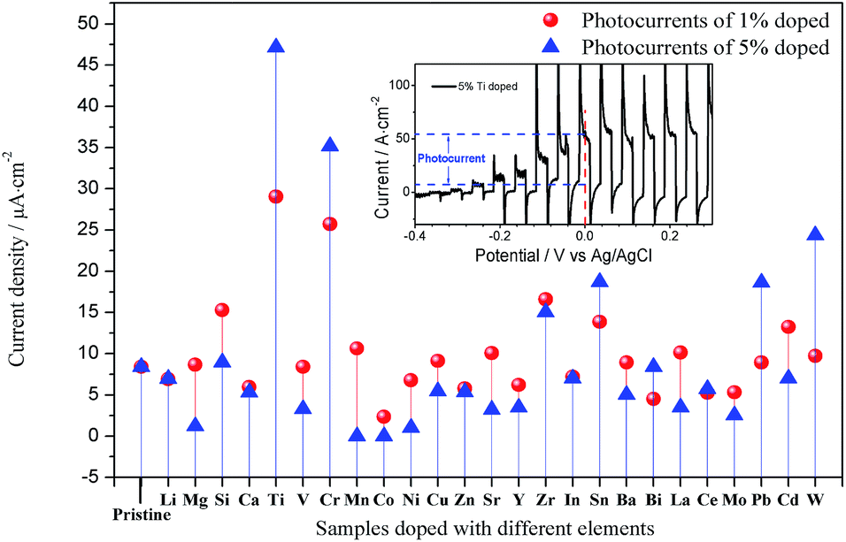 | ||
| Fig. 1 Photocurrent comparison of bare hematite photoelectrode and 1% and 5% metal element doped hematite photoelectrodes. The inset shows how the photocurrents were derived from the current–voltage (C–V) curves. | ||
It can be found that the pristine hematite photoelectrode showed a relatively low photocurrent, which is about 8.6 μA cm−2 at 0 V vs. Ag/AgCl. When comparing to the doped hematites, it is revealed that most elements doping show positive effect on photocurrents and among these dopants tested Ti gives the highest enhancement in photocurrent of hematite (about 47 μA cm−2), followed by Cr, W, Pb, Sn, Zr, etc. In particular, 5% doping level gives more enhancement than 1% doping level for the top 5 samples with highest photocurrents. While for other samples, those with 1% doping level give higher or similar photocurrent than those with 5% doping level. This result indicated that more effective dopants possess a higher optimal doping level. The decrease of photocurrent with higher doping level could result from exceeding dopants acting as recombination center. For those effective dopants, however high doping concentration does not act as recombination but make positive contribution to the photocurrent.
To look into the detailed influence from the different elements doping, those doped samples with top 7 performances were selected for further investigation. Fig. 2 presents the SEM images of flat-shaped hematite films. Apparently, the undoped hematite film consists of leaf shape particles with 30–50 nm in width and 120–150 nm in length. For hematite films doped with Cr, Ti, W, Sn, Zr or Pb, no obvious morphology change could be observed. The thickness of flat-shaped hematite film is determined to be around 100 nm.
 | ||
| Fig. 2 SEM images of (a) undoped (b) 5% Cr doped (c) 5% Ti doped (d) 5% W doped (e) 5% Sn doped (f) 5% Zr (g) 5% Pb doped flat-shaped hematite photoelectrodes. | ||
The chemical state of doped hematites identified by XPS spectra can be used to understand the chemical valence and bonding situation of elements. The original and fitted XPS spectra of the O 1s collected for pristine and doped hematite films are shown in Fig. 3. In O 1s XPS spectra, the pristine film shows a main peak at 529.7 eV, which is a characteristic peak of lattice oxygen in Fe2O3. The small peak at 531.2 eV is due to absorbed hydroxyl group on the surface of hematite. After doping treatment, the main peaks of all doped films shift to higher binding energy, similar as the previous reports.28 The foreign dopant atoms would exert influence on the Fe–O lattice and increased the binding energy. Fig. S1† shows the XPS spectra of each dopant and their valence states and molar ration to Fe were calculated and shown in Table S1.† Since the valence of Cr and Pb (+3 and +2, respectively) were not higher than Fe, the shift of O 1s peak to higher binding energy is relatively smaller. The peak around 532.8 eV for Ti, Pb and W doped samples can be ascribed to oxygen of SiO2, this could be from the exposed glass substrate. In Fig. S2,† two typical Fe 2p1/2 and Fe 2p3/2 peaks appear in all the samples and the absence of Fe2+ satellite peak at around 716 eV indicates that the main state of Fe is Fe3+.29
 | ||
| Fig. 3 O 1s XPS spectra of bare and doped planar-shaped hematite. | ||
The spin coating deposition is a facile method to prepare metal ion doped hematite with precise doping level and provide a rapid screen of doping elements for efficient dopants. However, the synthesized planar hematite thin films showed very low activities. The most reported hematite photoanodes with high photocurrents are Fe2O3 nanowire arrays. To check the role of different metal element doping in this hematite structure, we further selected typical dopants to compare their effects on Fe2O3 nanowire arrays. The elements of Ti, Sn, Zr, Pb, Mo and Ce with improved or decreased photocurrent in planar hematite were selected.
The nanorod arrays were prepared using a hydrothermal method in previous report.27 The doping procedure was conducted by soaking in dopant solution followed with heat treatment. In this work, we adopted a short-time annealing process (800 °C for 90 s) to induce surface dopants diffusion into hematite and prevent Sn of the FTO substrates from diffusing into hematite nanorods, which has been demonstrated in our previous report.24 Fig. 4 shows SEM images of annealed hematite nanorods doped with different dopants. It was found that the undoped nanorods were 80 nm in diameter and about 500 nm in length perpendicular to the FTO glass substrate, similar with previous reports.26 For the doped samples, there is no significant change in morphology of hematite nanorods after doping with Mo, Pb, Ce, Zr and Ti elements. While the Sn doping treatment make the surface of nanorods capped with small particles which can be due to the formation of SnO2 particles. As the Sn atom is relatively large compared to other dopants, it is more difficult to incorporate at interstitial sites or to diffuse into the hematite host.
 | ||
| Fig. 4 Low- and high-magnification SEM images of pristine and various metal element doped hematite nanorod arrays and cross-section SEM image of pristine hematite. | ||
X-ray diffraction (XRD) measurements were conducted to examine the phase purity and crystallinity of each sample. As shown in Fig. 5, the peaks of all films can be indexed to α-Fe2O3 with a rhombohedral structure (JCPDS card no. 24-0072). In the patterns of all films apart from FTO, the dominant hematite peak is (110) as a result of the (110) preferential orientation, which also consists with previous reports.24 There are no peak shifts or other phases exist in all the spectra. This result suggests that the doping has little effect on the crystal structure of hematite films and no detectable structure phase formed, including the amorphous SnO2 particles which are visible in SEM images.
 | ||
| Fig. 5 XRD patterns collected for bare Fe2O3 and element doped Fe2O3 nanorod photoelectrodes. | ||
Fig. 6 presents the PEC performance of pristine Fe2O3 and Fe2O3 nanorods doped with different elements. It can be observed that the hematite nanorod films show much more positive onset potentials than planar hematite films. The pristine Fe2O3 nanorods exhibit a photocurrent density of 37 μA cm−2 at 1 V vs. Ag/AgCl. After being doped with foreign elements, significant improvements of photocurrents were observed for most doped nanorods. In consistency with result of planar samples, the Ti doped hematite nanorod exhibits the highest photocurrent. Similarly, Zr, Sn, and Pb doped hematite nanorods also show greatly improved photocurrent response and the Mo doped sample produce a decreased photocurrent. While the Ce doped hematite showed an increased photocurrent, which is different from that of planar one.
 | ||
| Fig. 6 Photocurrent responses of bare and doped hematite nanorods recorded under chopped light irradiation. The electrolyte is 0.5 M Na2SO4 aqueous solution. | ||
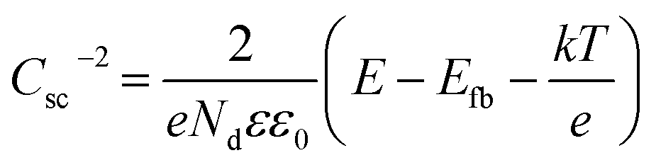
To investigate the effect of dopants on the electrochemical properties, the Mott–Schottky plots of pristine and doped hematite nanorod were tested in 0.5 M Na2SO4 aqueous solution. The flat band potential and carrier densities of films can be estimated from the Mott–Schottky eqn (1):26,30,31
 | (1) |
 | ||
| Fig. 7 Comparison of photocurrents, flat-band potentials and carrier densities of planar shaped hematite. | ||
In particular, the carrier density of Ce doped sample was increased but its flat band potential shifted negatively, resulting a reduced photocurrent. While for Sn doped hematite, the positively shifted flat-band potential induced an enhanced photocurrent even though its carrier density was decreased. It can be seen that the PEC performance of hematite photoelectrode is greatly related to flat band potential and carrier density which involves surface states and charge transport property, respectively. In general, a positively shifted flat-band potential is required and a decreased carrier density need to be avoided for an efficient PEC performance.
Valence band XPS spectra were recorded to determine the valence-band edge.36 The valence band XPS spectra for different element doped hematite nanorods were plotted and shown in Fig. S4† and the valence-band edge values were listed in Table S3.† It was found that the ranking of valence-band position with different element doped samples is similar to the results of flat band potential. It is easy to understand that the flat-band potential is close to the conduction band (CB) position for n-type semiconductor, and the difference between the valence band (VB) position and CB is band gap energy.37 Same trend for photocurrent and valence band edge of samples with different elements doping was observed. More specifically, samples with a more positive binding energy of valence band edge show a higher photocurrent. This result again verified that the shift of band edge position upon doping is an important factor that determined the photocurrent.
The improvement of photocurrent by the positively band edge position shift could be a result of improved surface reaction or surface charge transfer. To get more information of this process, electrochemical impedance spectroscopy (EIS) of both undoped and doped films were recorded. As shown in Fig. 8, the representative Nyquist plots for all hematite films can be fitted to a 2-RC-circuit model which consists of the resistance of FTO, Rs, the charge transport resistance in the bulk, RCT1, and the space-charge capacitance, CPE1, of the bulk hematite, as well as the Helmholtz capacitance at the hematite/electrolyte interface, CPE2, and the charge transfer resistance at the hematite/electrolyte interface, RCT2.18 The calculated equivalent circuit parameters by fitting according to the equivalent circuits are shown in Table 1. As can be observed, all doped hematite samples show reduced charge transport resistance in the bulk in comparison with the bare hematite. According to the Mott–Schottky results, the carrier density didn't increased much after doping, but the electrical conductivities of hematites upon doping improved, this could be explained by increased polaron hopping probability (the conducting mechanism of hematite) with lattice strain (shorter intraplane Fe–Fe distance) originated from the incorporated dopants.38 Further, the lowest bulk charge transport resistance was observed with Ti–Fe2O3 photoelectrode, followed by Zr–Fe2O3 and Sn–Fe2O3, in agreement with the photocurrent response. It is interesting to note that Mo–Fe2O3 photoelectrode shows lower bulk charge transport resistance but much higher resistance at the hematite/electrolyte interface, which can be responsible for the low photocurrent density.
 | ||
| Fig. 8 Electrochemical impedance spectra (EIS) for bare and doped hematite nanorod photoelectrodes measured at 1.0 V vs. Ag/AgCl under AM 1.5 G irradiation. The inset is the equivalent circuit model used for fitting the Nyquist plots. | ||
| Sample | RS (Ω cm−2) | CPE1 (F cm−2) | RCT1 (Ω cm−2) | CPE2 (F cm−2) | RCT2 (Ω cm−2) |
|---|---|---|---|---|---|
| Bare Fe2O3 | 78.35 | 2.73 × 10⁻⁵ | 1768.0 | 4.20 × 10⁻⁶ | 879.7 |
| Mo–Fe2O3 | 64.83 | 1.74 × 10⁻⁷ | 231.1 | 1.09 × 10⁻⁵ | 16340.0 |
| Pb–Fe2O3 | 71.99 | 1.08 × 10⁻⁷ | 361.0 | 7.57 × 10⁻⁵ | 664.3 |
| Ce–Fe2O3 | 68.94 | 1.13 × 10⁻⁵ | 505.6 | 1.26 × 10⁻⁴ | 729.0 |
| Sn–Fe2O3 | 72.45 | 1.49 × 10⁻⁵ | 146.7 | 2.63 × 10⁻⁴ | 266.9 |
| Zr–Fe2O3 | 66.14 | 1.30 × 10⁻⁵ | 122.9 | 2.87 × 10⁻⁴ | 259.8 |
| Ti–Fe2O3 | 73.68 | 3.46 × 10⁻⁵ | 89.53 | 2.66 × 10⁻⁴ | 363.1 |
Conclusions
In summary, we have reported synthesis of planar and nanorod shaped hematite electrodes doped with various metal atoms and investigation of the effect of metal doping on the physical, chemical and PEC properties. The performances of doped planar hematite thin films were compared under the same synthetic and measurement condition. The Ti, Cr, W, Pb, Sn and Zr were found to be the most efficient dopants to improve the PEC performance. Samples doped with these elements were further investigated for their morphological and electronic properties. For widely investigated nanorod arrays shaped hematite were also doped with selected dopant elements. The result showed that Ti, Zr, and Sn doping greatly improve the photocurrent, followed with Ce and Pb doping which also increased the photocurrent. The Mo doping however had a negative effect on the PEC property of hematite photoelectrodes. Mott–Schottky plots indicated that the charge carrier densities were not changed for most dopants. Valence band XPS spectra samples with a more positive binding energy of valence band edge show a higher photocurrent. Electrochemical impedance spectroscopy showed that the doped hematite samples show reduced charge transport resistance. These results demonstrated that the improvement of PEC performance of doped hematite is largely due to their positively shifted flat band potential, which influenced the surface charge transport property. This result provides us new explanation on the effect of doping on hematite photoelectrodes.Acknowledgements
This work was supported by the National Natural Science Foundation of China (No. 51202186, 51236007, 21606175).References
- K. Sivula, F. Le Formal and M. Graetzel, ChemSusChem, 2011, 4, 432–449 CrossRef CAS PubMed.
- Y. Yang, M. Forster, Y. Ling, G. Wang, T. Zhai, Y. Tong, A. J. Cowan and Y. Li, Angew. Chem., Int. Ed., 2016, 55, 3403–3407 CrossRef CAS PubMed.
- P. Zhang, T. Wang, X. Chang, L. Zhang and J. Gong, Angew. Chem., 2016, 55, 5851–5855 CrossRef CAS PubMed.
- P. Peerakiatkhajohn, J. H. Yun, H. Chen, M. Lyu, T. Butburee and L. Wang, Adv. Mater., 2016, 28, 6405–6410 CrossRef CAS PubMed.
- A. Murphy, P. Barnes, L. Randeniya, I. Plumb, I. Grey, M. Horne and J. Glasscock, Int. J. Hydrogen Energy, 2006, 31, 1999–2017 CrossRef CAS.
- J. Wang, J. Su and L. Guo, Chem.–Asian J., 2016, 11, 2328–2334 CrossRef CAS PubMed.
- J. Wang, N. Zhang, J. Su and L. Guo, RSC Adv., 2016, 6, 41060–41066 RSC.
- F. Malara, F. Fabbri, M. Marelli and A. Naldoni, ACS Catal., 2016, 6, 3619–3628 CrossRef CAS.
- I. Cesar, K. Sivula, A. Kay, R. Zboril and M. Graetzel, J. Phys. Chem. C, 2009, 113, 772–782 CAS.
- C. Toussaint, H. L. L. Tran, P. Colson, J. Dewalque, B. Vertruyen, B. Gilbert, N. D. Nguyen, R. Cloots and C. Henrist, J. Phys. Chem. C, 2015, 119, 1642–1650 CAS.
- L. Wang, X. Zhou, N. T. Nguyen and P. Schmuki, ChemSusChem, 2015, 8, 618–622 CrossRef CAS PubMed.
- J. Y. Kim, G. Magesh, D. H. Youn, J. W. Jang, J. Kubota, K. Domen and J. S. Lee, Sci. Rep., 2013, 3, 2681 Search PubMed.
- S. C. Warren, K. Voitchovsky, H. Dotan, C. M. Leroy, M. Cornuz, F. Stellacci, C. Hebert, A. Rothschild and M. Gratzel, Nat. Mater., 2013, 12, 842–849 CrossRef CAS PubMed.
- P. Peerakiatkhajohn, J. H. Yun, H. J. Chen, M. Q. Lyu, T. Butburee and L. Z. Wang, Adv. Mater., 2016, 28, 6405–6410 CrossRef CAS PubMed.
- N. T. Hahn and C. B. Mullins, Chem. Mater., 2010, 22, 6474–6482 CrossRef CAS.
- J. Deng, J. Zhong, A. Pu, D. Zhang, M. Li, X. Sun and S.-T. Lee, J. Appl. Phys., 2012, 112, 084312 CrossRef.
- S. Shen, J. Jiang, P. Guo, C. X. Kronawitter, S. S. Mao and L. Guo, Nano Energy, 2012, 1, 732–741 CrossRef CAS.
- N. Mirbagheri, D. Wang, C. Peng, J. Wang, Q. Huang, C. Fan and E. E. Ferapontova, ACS Catal., 2014, 4, 2006–2015 CrossRef CAS.
- H. Pan, X. Meng, D. Liu, S. Li and G. Qin, Phys. Chem. Chem. Phys., 2015, 17, 22179–22186 RSC.
- D. Wang, H. Chen, G. Chang, X. Lin, Y. Zhang, A. Aldalbahi, C. Peng, J. Wang and C. Fan, ACS Appl. Mater. Interfaces, 2015, 7, 14072–14078 CAS.
- Y. C. Zhang, S. Q. Jiang, W. J. Song, P. Zhou, H. W. Ji, W. H. Ma, W. C. Hao, C. C. Chen and J. C. Zhao, Energy Environ. Sci., 2015, 8, 1231–1236 CAS.
- W. D. Chemelewski, O. Mabayoje, D. Tang, A. J. Rettie and C. B. Mullins, Phys. Chem. Chem. Phys., 2016, 18, 1644–1648 RSC.
- J. Huang, G. Hu, Y. Ding, M. Pang and B. Ma, J. Catal., 2016, 340, 261–269 CrossRef CAS.
- J. Wang, B. Feng, J. Su and L. Guo, ACS Appl. Mater. Interfaces, 2016, 8, 23143–23150 CAS.
- D. D. Qin, Y. L. Li, T. Wang, Y. Li, X. Q. Lu, J. Gu, Y. X. Zhao, Y. M. Song and C. L. Tao, J. Mater. Chem. A, 2015, 3, 6751–6755 CAS.
- Y. Ling, G. Wang, D. A. Wheeler, J. Z. Zhang and Y. Li, Nano Lett., 2011, 11, 2119–2125 CrossRef CAS PubMed.
- L. Vayssieres, N. Beermann, S. E. Lindquist and A. Hagfeldt, Chem. Mater., 2001, 13, 233–235 CrossRef CAS.
- Q. Li, J. Bian, N. Zhang and D. H. L. Ng, Electrochim. Acta, 2015, 155, 383–390 CrossRef CAS.
- Y. Ling, G. Wang, J. Reddy, C. Wang, J. Z. Zhang and Y. Li, Angew. Chem., Int. Ed., 2012, 51, 4074–4079 CrossRef CAS PubMed.
- A. G. Tamirat, W. N. Su, A. A. Dubale, H. M. Chen and B. J. Hwang, J. Mater. Chem. A, 2015, 3, 5949–5961 CAS.
- Y. B. Chen, Z. X. Qin, T. Chen, J. Z. Su, X. Y. Feng and M. C. Liu, RSC Adv., 2016, 6, 58409–58416 RSC.
- G. Wang, Y. Ling, D. A. Wheeler, K. E. George, K. Horsley, C. Heske, J. Z. Zhang and Y. Li, Nano Lett., 2011, 11, 3503–3509 CrossRef CAS PubMed.
- F. Boudoire, R. Toth, J. Heier, A. Braun and E. C. Constable, Energy Environ. Sci., 2014, 7, 2680–2688 CAS.
- Q. Li, J. C. Bian, N. Zhang and D. H. L. Ng, Electrochim. Acta, 2015, 155, 383–390 CrossRef CAS.
- O. Zandi, B. M. Klahr and T. W. Hamann, Energy Environ. Sci., 2013, 6, 634–642 CAS.
- E. A. Kraut, R. W. Grant, J. R. Waldrop and S. P. Kowalczyk, Phys. Rev. Lett., 1980, 44, 1620–1623 CrossRef CAS.
- Q. L. Xu, J. G. Yu, J. Zhang, J. F. Zhang and G. Liu, Chem. Commun., 2015, 51, 7950–7953 RSC.
- M. N. Huda, A. Walsh, Y. F. Yan, S. H. Wei and M. M. Al-Jassim, J. Appl. Phys., 2010, 107, 123712 CrossRef.
Footnote |
| † Electronic supplementary information (ESI) available: XPS spectra, Mott–Schottky plots, valence band spectra and tables for summary of electronic parameters. See DOI: 10.1039/c6ra22895j |
| This journal is © The Royal Society of Chemistry 2016 |