Zhonghai Lin‡
*a,
Zhi Yang‡b,
Pingjian Wanga,
Guangfen Weia,
Aixiang Hea,
Wen Guoa and
Minqiang Wang*b
aKey Laboratory of Intelligent Information Processing in Universities of Shandong, Shandong Business and Technology University, Yantai, 264005, China. E-mail: zhonghailin@sdibt.edu.cn
bElectronic Materials Research Laboratory (EMRL), Key Laboratory of Education Ministry, International Center for Dielectric Research (ICDR), Xi'an Jiaotong University, Xi'an 710049, China. E-mail: mqwang@mail.xjtu.edu.cn
First published on 27th October 2016
Lead chalcogenide colloidal quantum dots (CQDs) offer promise in infrared photodetectors due to their narrow bandgap and quantum size effect. Compared with PbS and PbSe CQDs, PbTe CQD has received the least attention because it is much easier oxidized in air owing to weak binding energy and hard size control is not in favor of observing quantum confinement effect. Here we developed a layer-by-layer method to prepare PbTe CQD photodetectors with the assistance of the inorganic halide ligand (TBAI) treatment. The results show that TBAI treated PbTe CQD film photodetectors have high photocurrent and short response time (0.39 ms) and recovery time (0.49 ms), indicating the effectiveness of TBAI treatment on PbTe CQD film. We also find PMMA protector is necessary to obtain stable photoresponse performance for TBAI treated PbTe CQD film photodetectors in air.
A critical component of the progress listed above is the incorporation of halide and sulfide ligands into the CQDs. Although the charge carrier mobility of CQD films has been improved impressively by the use of sulfide ligands, there is a finding ascribed to these solids' high density of defects.12 To reduce defect density while keep high carrier mobility, halide ligands have been explored for CQD passivation. The atomic sizes of halide ligands allow efficient carrier transportation between CQDs, while the strong binding of halides to CQD surfaces offers the capacity to improve surface passivation.14 Since the use of a protic solvent in solid-state ligand exchange can cause the loss of ligands,15 it was crucial to develop new ligands that could bind more strongly to CQD surfaces, resisting these solvents. In comparison to bromide and chloride ligands, iodide ligands were found to form stronger bonds to the CQD surface atoms.16 The use of iodide ligands could lower film defect density greatly. These experimental results were explained via soft/hard base/acid theory: the soft base iodide bound strongly to soft acid lead atoms on PbS CQDs, while hard acid hydrogen cations bound strongly to hard base chloride.14,17 TBAI is one of iodine-containing ligands. It demonstrates the strong bonding character of iodine to the surface of lead chalcogenide CQDs and promote carrier transportation and lower the defect density in PbS and PbSe devices.5 E. H. Sargent's group has done a series of research works on CQD solar cells by that using tetrabutylammonium iodide (TBAI) treated CQD layer acts as a main charge generation layer.18–24 Power conversion efficiency was notably enhance to 10.8%.24 Furthermore, researchers have demonstrated the strong bonding character of TBAI ligands to the surface of lead chalcogenide CQDs (PbS, PbSe) and might be responsible for the lessened sensitivity to oxygen.5,25 PbTe with a larger average exciton Bohr radius (∼46 nm) and lighter e− and h+ masses (0.22 and 0.24m0 respectively) than PbSe, is potentially even more size tunable than PbSe and PbS, and a more promising candidate from which to build electronically active solids because of its large dielectric constant (ε0 ∼ 1000), which should substantially reduce the Coulomb charging energy of the PbTe nanocrystal array.26,27
Among IR-active CQD optoelectronic materials, PbTe CQDs have received the least attention, compared with other lead chalcogenide PbS and PbSe CQDs, and the bonding length of PbTe is the largest owing to weak binding energy between Pb and Te. In addition, large surface activity of CQDs makes PbTe CQD very easy to oxidize in air, so bad environmental stability makes their photoconductor performance degrade very quickly until disappear in air.28 The PbTe has large Bohr radius, making it good candidate for the research on quantum size effect. However, the precisely size control of PbTe CQDs is very difficult, making narrow bandwidth of exciton absorption peak is hard to obtain, so many properties arising from quantum confinement effect are hard to observe. Our group has reported a rapid injection solution-phase synthesis route for the preparation of monodispersed PbTe CQDs.29
In this report, we prepared PbTe CQD film photodetector by solution-processed method in inert atmosphere at room-temperature. The PbTe CQDs thin film was fabricated on the plasma-treated Si/SiO2 substrate with interdigital Ti/Au electrodes using a layer-by-layer spin-coating method. The PbTe CQDs thin films with 2.5 nm-long oleate ligands (OA) are highly insulating and not applicable as photoconductive devices. The introduction of TBAI on PbTe CQDs has improved passivation of the PbTe QD surface, and promoted carrier transportation and lower the defect density of the PbTe QD thin film. Next, we exhibited the TBAI ligand exchange minimizes the PbTe CQDs spacing. Moreover, we measured and analyzed the infrared photoelectric properties of PbTe CQD device. The response time (0.39 ms) and recovery time (0.49 ms) are quite outstanding. We believe the success of chemical treatment using halide ligands can greatly expand the potential application areas of infrared PbTe CQD photodetector.
:
octane, 4
:
1 by volume).
:
YAG NIR laser (1064 nm, 120 mW cm−2) were employed to evaluate the full spectrum and single spectrum photoresponse of PbTe CQD photodetector, respectively. The dark current, light current and the time-dependent photoresponse were recorded by a Keithley 2400 source meter. To determine the response and recovery time accurately, we used a pulsating source by keeping a mechanical chopper rotating at different frequencies in front of a continuous NIR laser. Then we could obtain the transient voltage across 20 MΩ resistance connected in series by using the digital phosphor oscilloscope (Tektronix DPO 4104). All measurements were conducted in air.
XPS was used to identify the effects of TBAI treated PbTe CQD film, as shown in Fig. 2. The general scan spectrum shows that the TBAI treated PbTe CQD film has stronger intensity for all elements than as-made. From elemental spectra, we can confirm the successful incorporation of iodine onto the CQDs due to the existence of strong I 3d peak in TBAI treated PbTe CQDs film. The standard peaks of Pb 4f are 137 eV and 142 eV, which is assigned to Pb(4f7/2) and Pb(4f5/2), respectively.31 The TBAI treated CQD film has the same Pb 4f peaks position, while as-made CQD film has a big shift, which may be attributed to PbOx peak.32 In addition, from Te 3d spectrum, we can see 571.7 eV (3d5/2) and 582 eV (3d3/2) for both as-made and TBAI treated CQD films, and high energy peaks for as-made are assigned to TeO2. Te 3d peaks are consistent with N. Ziqubu et al. experimental datas.33 So the severe oxidized state was demonstrated in as-made PbTe CQD film, and TBAI treated is quite helpful to overcome oxidized process, indicating the good passivation effect from TBAI treatment.
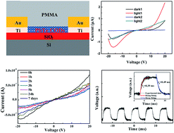
PbTe CQDs were spin-coated onto the plasma-treated Si/SiO2 substrate with interdigital Ti/Au electrodes (see Fig. S3†). We then fabricated PbTe CQD photodetector with the structure shown in Fig. 3a. To build photodetector devices, we prepared PbTe CQD thin film with different thickness. The top view and cross-sectional SEM images of the representative PbTe–TBAI CQD thin film were shown in Fig. 4b, c and S4.† We can see clear PbTe CQDs grain and bright area from top and cross-sectional view, respectively, resulting from improving conductivity due to TBAI treatment. The thickness of PMMA layer is about 2 μm.
In order to obtain good photoresponse performance, we have prepared TBAI treated PbTe CQD film with different thickness, and related thickness was obtained from cross-section SEM image in Fig. S5.† From Fig. 4, we can see obvious electrical property change from nonlinear Schottky contact to symmetric linear ohmic contact except for PbTe CQD film with 47 nm thickness. According to equation
, responsivity can be calculated as 0.13 mA W−1, 1 mA W−1, 1.6 mA W−1 and 1.9 mA W−1 for four devices with increasing thickness, respectively. In addition, with increasing thickness, we can see both increasing dark current and photocurrent, attributing to increasing photo-generated carriers number due to increasing light absorption. The working mechanism of photoconductor detector is based on three processes: the generation of photocarriers, the charge injection from external circuit and charge transportation in polycrystalline CQD film. Based on previous reports,32 the chemical ligand exchange can play a significant role for charge injection and transportation. In particular, the TBAI treatment has already been demonstrated to improve conductivity and stability of CQD film successfully through surface passivation. Oh et al. investigated the effect of different chemical ligand treatment on the charge injection and transportation of PbSe CQD film.30 According to Mott–Schottky theory, the barrier height for electron injection is determined by the metal work function and the semiconductor electron affinity, and electron affinity of CQDs can be great affected by surface ligands. Based on previous reports on PbS QDs, TBAI treated PbS QDs film exhibited air-stable n-type,16 while EDT treated PbS QDs film exhibited p-type.25 For our TBAI treated PbTe CQD film, the fresh sample has Schottky contact because the barrier between the high work function Au and n-type TBAI treated PbTe CQD film. However, after some time, it is changed to ohmic contact because p-type PbTe CQDs film is obtained due to CQDs surface oxidized partially. So we think the Schottky to ohmic contact transform is caused by the conversion from original n-type to p-type of PbTe CQD film. In order to further confirm above speculation, we conduct stability measurements for PbTe CQD film photodetectors with and without PMMA layer. From Fig. 5a and b, we can see almost unchanged dark current from the beginning to 7 days for photodetector with PMMA protective, while the photocurrent is decreasing gradually from the beginning to 5 h, then it can increase to a stable value after 24 h. Compared with that, from Fig. 5c and d, we can see gradually increased dark current and photocurrent from the beginning to 5 h for photodetector without PMMA protective, but it can decrease a little after 24 h, and photoresponse is disappeared when this photodetector is stored in air after 7 days. In addition, the Schottky contact can be preserved for a long time for photodetector with PMMA protective, while it is the ohmic contact for that without PMMA protective from the beginning. This stability measurement can illustrate that the oxidized process play a key role in both charge injection and transportation processes. Specifically, oxidized state existed on PbTe CQDs surface causes the change of barrier height between electrode and film, resulting in conversion from Schottky contact to ohmic contact, and film conductivity also can be improved upon air exposure because oxidized state is a kind of p-type doping for PbTe CQDs, increasing the carriers concentration, but finally very low conductivity will appear due to insulating PbOx or TeO2 shell after very long air exposure. This result is in accordance with previous reports on PbSe CQD film by Nozik's group.34,35 Our stability results also indicate that TBAI treatment is not enough to protect PbTe CQDs from oxidize in air, while TBAI treated PbS CQD film can achieve air-stable,16 indicating that PbTe CQDs are oxidized much easier than PbS CQDs. So PMMA protector is necessary to obtain stable photoresponse performance for TBAI treated PbTe CQD film photodetectors in air.
The multi-cycle time-dependent photoresponse measurements are an important route to evaluate photoresponse repeatability and obtain accurate response and recovery time. Fig. 6a shows a schematic setup for time-dependent photoresponse measurement. We can observe the alternating voltage from series resistance by oscilloscope under pulsating laser, indicating the photoresponse process of photodetector. The response time (tr) and recovery time (td) are defined as the time taken by the signal to reach 63% and 37% of the steady photovoltage according to previous report.36 From Fig. 6b and S6,† we can see good photoresponse repeatability and obvious wave shape evolution by increasing pulsating light frequency, and steady photovoltage can always be obtained before the frequency reaches to 220 Hz. Here we can obtain accurate response time 0.39 ms and recovery time 0.49 ms by fitting single photoresponse cycle at frequency of 150 Hz. These very short times are quite outstanding compared with our previous PbTe CQD photodetector37 and other CQD photodetectors with the similar structure.33,38 The response and recovery time can be affected by many factors, such as crystal boundary size and barrier height, surface property of QDs, carrier mobility of QDs film and carrier transportation length and so on. We attributed the main reason for this ultrafast response to good surface passivation of QDs from TBAI and short carrier transportation length.
Footnotes |
| † Electronic supplementary information (ESI) available. See DOI: 10.1039/c6ra22581k |
| ‡ These authors contributed equally to the work. |
| This journal is © The Royal Society of Chemistry 2016 |