Integration of p-type β-In2S3 thin films on III-nitride heterostructures for multiple functional applications

Hongfei Liu*, Qingqing Dou and Chin Sheng Chua
Institute of Materials Research and Engineering (IMRE), A*STAR (Agency for Science, Technology and Research), 2 Fusionopolis Way, Singapore 138634, Singapore. E-mail: liuhf@imre.a-star.edu.sg

Received 9th September 2016 , Accepted 26th September 2016

First published on 28th September 2016


Abstract

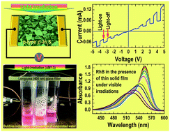
We report on the conversion of n-type InN thin films on top of III-nitride heterostructures to p-type β-In2S3 by post-growth heat treatments in a sulfur-vapor environment and address their photoelectrical and photocatalytic properties for functional integrations. Their electrical, structural, and spectroscopic evolutions as a function of sulfurization temperatures reveal an onset of surface passivation of InN at low temperatures (i.e., T < 550 °C) and the passivation is less effective at high temperatures. The conversion of InN to β-In2S3 starts at T ≥ 700 °C; the conversion increases with the sulfurization temperature and completes at T = 750 °C; and a further increase in the sulfurization temperature leads to a conversion of β-In2S3 to In2O3 due to the exhaustion of sulfur. The coherently strained InGaN buffer underneath the InN overlayer of the heterostructure is intact even at T = 800 °C. Photocurrent measurements do not show any apparent light responses for the thin films until sulfurized at T ≥ 700 °C while the photocatalytic degradation tests of rhodamine B (RhB) under visible irradiations (λ ≥ 400 nm) provide evidence for deethylation of RhB to DMRh (N,N-diehyl-N′-ethyl-rhodamine 110) on the surface of the thin films with higher activities on n-type InN and In2O3 than that on p-type β-In2S3 films. These observations, together with the intact InGaN underneath, open up a novel way to monolithic integrations of β-In2S3/InN based optical/photochemical sensors with GaN-based electronic devices (e.g., high-electron-mobility transistors) for advanced applications.


I. Introduction

The monolithic integration of functional materials, such as metal oxides and sulfides, with conventional semiconductors for fabricating unique devices with novel functions and/or improved performances has been extensively explored and investigated in recent years.1–4 However, the incompatibility of oxygen and sulfur with conventional III–V semiconductor growth techniques, e.g., molecular beam epitaxy (MBE) and metalorganic chemical vapor deposition (MOCVD), makes the in situ integration impracticable. In this light, post-growth processing is usually employed. The post-growth processing can be, for example, to deposit desired layers of additional material in a separated rector. Alternatively, it can be conversion of an in situ grown additional layer to desired ones by heat treatments in a controlled atmosphere. From the cost and production point of view, the material conversion method is more favorable since in the latter case a separate deposition equipment/reactor is required which is usually more expensive than the simple heat treatment equipment.

Our recent studies revealed that GaAs epiready wafers can be partly converted to layered Ga2S3 via heat treatment under a sulfur vapor environment in a horizontal tube-furnace. This process is otherwise known as thermal vapor sulfurization (TVS).5 The obtained Ga2S3/GaAs heterostructures exhibit great photosensing and light-driven water splitting properties.4 Compared with Ga2S3, In2S3 has a smaller bandgap, which is of great interest in photovoltaic applications for replacing the toxic CdS.6,7 In general, In2S3 can be crystallized in α-(cubic), β-(defective spinel), and γ-(layered hexagonal) structures. Among them, β-In2S3, has long been studied for electrical, optoelectronic, and photoelectrochemical applications, all related to its defective spinel structure and the direct bandgap of ∼2.3 eV.8–11

In this work, InN thin films of about 200 nm thick on top of InGaN/GaN heterostructures are studied upon TVS towards the integration of β-In2S3 with GaN-based III-nitride semiconductors. Such integrations are desired for fabricating functional devices, e.g., high performance photochemical sensors, which can work in harsh environment with high stability. The InN thin films were grown by MOCVD on c-plane sapphire substrates using a GaN template followed by indium-composition-stepped InGaN buffer layers, i.e., the nitrides stacked in InN/InGaN-ii/InGaN-i/GaN. High-resolution X-ray diffraction (HRXRD) studies revealed that the InGaN-i buffer layer is coherently strained on the GaN template and its indium composition is about 16.1% while the InGaN-ii layer is completely relaxed and its indium composition is about 57.0%.3,12

II. Experimental method

The InN thin film was diced into small pieces of ∼8 × 8 mm2 followed by a sequenced sonication in acetone, isopropanol, and deionized water for a few minutes. After sonication, the samples were blow-dried with nitrogen and ready for TVS process. The TVS process is carried out in a horizontal tube-furnace with nitrogen and sulfur powder as the carrier gas and the sulfur source, respectively. The InN film was located, facing-up, at the center of the hot zone while the sulfur powder was located at the upstream of the nitrogen gas flow. After loading the sulfur source and the InN film, the tube chamber was purged with nitrogen for 2 hours at a flow rate of 460 sccm. To initiate the TVS, the nitrogen flow rate was decreased to 100 sccm and the hot zone temperature was increased to a target value T, which ranges from 450 to 800 °C. The hot zone temperature was kept at its set temperature T for 30 min. After the TVS process, the nitrogen flow rate was increased back to 460 sccm and the heating power was switched off. The reactor was allowed to naturally cool down before unloading of the TVS-treated samples.

Morphological, structural, and electrical properties evolutions of the TVS-treated InN thin films were characterized using scanning-electron microscopy (SEM), ultraviolet micro Raman scattering (325 nm laser excitation), HRXRD, and Hall-effect measurements (Bio-Rad HL5500). Elemental analyses were carried out by using energy-dispersive X-ray spectroscopy (EDX) and X-ray photoelectron spectroscopy (XPS). Photoluminescence (PL) measurements were carried out at room temperature in an automated PL system equipped with a 532 nm Nd:YAG laser; a charge-coupled device (CCD) and an InGaAs detector array were used for collecting the PL emissions in the ranges of 300–1200 nm and 800–1800 nm, respectively. Photocurrent was measured under a solar illumination (AM1.5). While the same light source was used for testing the photocatalytic reactions; a long-pass glass filter (cut-off wavelength at 400 nm) was used to filter off the UV portion. The contaminant used in the photocatalytic reactions is rhodamine B (RhB) with a concentration of 2 × 10⁻⁵ M. The character absorption peak of RhB at ∼555 nm was monitored and analyzed, using a UV-VIS-NIR spectrophotometer, as a function of reaction time.

III. Results and discussion

A. TVS-induced evolutions in electrical and morphological properties

The Hall-effect measurement results of the TVS-treated InN thin film samples are summarized in Table 1. Fig. 1 presents the SEM images recorded from the InN thin film samples before and after TVS at T = 450, 550, 600, 700, and 800 °C; the scale bars are of 500 nm. A comparison between the Hall-effect results in Table 1 and the morphological evolutions in Fig. 1 reveals that surface passivation of InN occurred at T = 450 °C without any morphology changes. This suggests that sulfur only reacted with the surface of InN at atomic thickness which reduced the surface accumulation of electrons and increased the electron mobility (see Table 1).13 However, the small changes in the carrier-mobility/density at T = 550 and 600 °C indicates that the surface passivation of InN is less effective at high temperatures. Onset of the morphology changes occurred at T = 550 °C [see the circular highlights in Fig. 1(c)] with small triangular facets emerging at T = 600 °C. The size and density of the triangular facets increases at T = 700 °C and completely replaced the brain-fold-like morphology of InN. This change in morphology is accompanied by a drastic decrease/increase in the carrier-mobility/resistivity. Both the electrical properties and the morphology evolutions suggest a phase transformation of the InN thin film, to possibly In2S3, upon TVS treatment at T ≥ 700 °C. The transformation to In2S3 is supported by the triangular facets which is consistent with the (111) crystal planes of β-In2S3.8,14 No changes in the morphology can be distinguished when T is increased from 700 to 750 °C (see ESI Fig. S1) while the triangular facet structures are replaced by irregular particles at T = 800 °C [see Fig. 1(f)]. The grain sizes are generally uniform distributed throughout the sample surface, for example, in the range of 150–200 nm for the sample treated at 700 °C. This value is larger than that estimated (∼80 nm) from XRD using Scherrer formula, indicating that the grains, in average, have a smaller thickness than the in-plane dimension. This is because the top-view SEM only shows the in-plane dimension while the XRD estimate the overall grain size that includes the vertical dimension, i.e., the grain thickness.
Table 1 Summary of Hall-effect measurements of InN thin films upon TVS at various temperatures for 30 min; the data variations of multiple measurements from a certain sample are smaller than 5% (i.e., the error bars are typically smaller than 5% of the individual measured values)
Samples Resistance (Ω □−1) Mobility (cm2 V−1 s−1) Carrier density (1014 cm−2)
As-grown 70 164 −5.4
T = 450 °C 110 280 −2.0
T = 550 °C 121 135 −3.8
T = 600 °C 119 176 −3.0
T = 700 °C 1460 14 −3.0
T = 750 °C 39[thin space (1/6-em)]080 4 +0.4
T = 800 °C 3427 7 −2.8


image file: c6ra22548a-f1.tif
Fig. 1 SEM images recorded from InN thin films before and after thermal vapor sulfurization (TVS) at elevated temperatures for 30 min. (a) As-grown, (b) TVS at 450 °C, (c) TVS at 550 °C, (d) TVS at 600 °C, (e) TVS at 700 °C, and (f) TVS at 800 °C. The scale bars are of 500 nm.

From the temperature studies of the TVS treatment, the most striking observation is the conversion of electrical conduction of the InN thin film from n- to p-type at T = 750 °C. This provides a clear-cut evidence for the TVS-induced phase transformation at elevated temperatures. Also, the sample is observed to exhibit n-type conductivity after TVS treatment at T = 800 °C. This result, together with the morphological changes from triangular facets (at T = 700 and 750 °C) to irregular particles (at T = 800 °C), suggests a separate phase transformation occurring at T = 800 °C. The p-type conductivity of β-In2S3 (see later sections for the phase identifications) is most likely caused by N atoms doping from the decomposition of InN. This is because N atoms, having one electron less than S in the outer electron orbitals, when replacing S at the lattice matrix of β-In2S3, exhibit p-type doping. The further conversion of p-type β-In2S3 to n-type In2O3 implies an ineffective doping of N in In2O3. This situation is quite similar to ZnO, where the p-type doping is very difficult to be realized via incorporating group-V atoms.15

B. Phase conversion verified by UV-Raman scattering and HRXRD

Fig. 2(a) presents the Raman scattering spectra collected from the InN thin films before and after TVS treatment at various temperatures using a 325 nm laser excitation. It is observed that the TVS treatment at 450 °C did not introduce any change to the Raman spectrum. At 550 °C, the TVS treatment introduced a background (in the range of 200–400 cm−1) and slightly broadened the EH2 mode of InN. Both the background in the range of 200–400 cm−1 and the feature broadening of EH2 are increased by the TVS at 600 °C. Drastic spectral changes occurred at T = 700 °C where the EH2 feature has vanished. Instead, six new Raman features (indicated by P1–P6) appeared in the range of 200–400 cm−1 along with broad bands at about 455, 615, and 710 cm−1. Likewise, the Raman spectrum of the sample after TVS at 800 °C is greatly different from those of the as-grown and the low-temperature treated (T ≤ 750 °C) InN films. These spectral evolutions strongly correlate with those of Hall-effect and SEM results discussed above, especially the transition point at T = 700 °C. Spectral fittings of the Raman features have been carried out for identifying the crystal structures. The fittings are presented in ESI (see Fig. S2 and S3) and the results are summarized in Table 2 together with those of β-In2S3 and body-center-cubic (bcc) In2O3 reported in the literature.16–18
image file: c6ra22548a-f2.tif
Fig. 2 (a) Ultraviolet Raman-scattering spectra and (b) HRXRD θ/2θ-scanning curves collected from the InN thin films before and thermal vapor sulfurization at various temperatures.
Table 2 Summary of the Raman features in cm−1 collected from InN thin films after TVS at 700 and 800 °C for 30 min, results of β-In2S3 (ref. 14) and bcc-In2O3 (ref. 14, 16 and 17) from literature are also presented for comparisons
T = 700 °C Ref. 14 T = 800 °C Sputtered Ref. 14 Ref. 16 Ref. 17
177 214.8 214.7 215
214.8 214 305.7 307.7 306 307 302
248.5 248 326.7 329.2 321
267.7 267 364.1 366.2 366 369 366
307.9 307 388.2 388.0 392
326.8 325 421.1 420.0
365.3 368 457.1 458.5 453 454
454.2 493.0 495.1 495 499 494
614.9 534.3 535.0
709.8 560.3 562.5
    595.9 594.0 589
    627.1 626.6 629 629


The comparisons presented in Table 2 suggest that the P2–P6 Raman features of β-In2S3 in Fig. 2(a) are A1g (248.5, 307.9, 365.3 cm−1), Eg (267.7 cm−1), and F2g (326.8 cm−1), respectively. The other four modes, seldom reported in the literature, are most likely due to defect- and/or disorder-induced modes (either localized modes or activated silent modes).19–21 For cubic In2O3, the eleven of the observed modes in Table 2 can be assigned to F2g (214.8, 305.7, 326.7, 364.1, 388.2, and 457.1 cm−1) and Ag (493.0, 534.3, 560.3, 595.9, and 627.1 cm−1) while the mode at 421.1 cm−1 is quite different from its closest potential candidate at about 400 cm−1.17 It is probably due to a defect/disorder-activated silent mode. The comparisons in Table 2 and the similarity between the Raman spectra collected from the InN thin film after TVS at 800 °C and that from a bcc-In2O3 thin film deposited by magnetron-sputtering (see Fig. S3)22 indicate that phase conversions of InN to β-In2S3 and bcc-In2O3 occurred at T = 700 and 800 °C, respectively.

The InN to β-In2S3 and bcc-In2O3 conversions have further been confirmed by HRXRD. The diffraction patterns are presented in Fig. 2(b), they were collected in a θ/2θ-scanning configuration, using GaN (0002) atomic planes as the reference for beam optimizations. The diffractions from β-In2S3 (311) and (222) (JCPDS 65-0459), InN/InGaN-ii/InGaN-i/GaN (0002), and body-center-cubic In2O3 (222) and (004) (JCPDS 06-0416) atomic planes have been identified. It can be observed that the diffraction peaks of InN/InGaN-ii/InGaN-i/GaN (0002) did not change their intensities at all until the TVS temperature is increased to T ≥ 700 °C. At T = 700 °C, the diffraction intensity of InN (0002) exhibits a significant decrease while those of InGaN-ii/InGaN-i/GaN (0002), located beneath InN, are intact. In addition, the diffractions of β-In2S3 (311) and (222) atomic planes appears (see the enlarged curves in ESI, Fig. S4). When T is increased to 750 °C, the diffraction peak of InN (0002) vanished and the diffraction intensity of InGaN-ii (0002) is significantly reduced. Also, the peaks for InGaN-i/GaN (0002) beneath InN/InGaN-ii remain intact while the diffraction peaks for β-In2S3 (311) and (222) increased in intensity and shifted to larger angles (see the ESI Fig. S4). The peak shifts of β-In2S3 (311) and (222) and the intensity reduction of InGaN-ii (0002), together with the asymmetric β-In2S3 (311) and (222) peaks at T = 750 °C (see the ESI, Fig. S4), suggest an increase in the thickness of β-In2S3 as well as incorporations of Ga atoms into the β-In2S3 crystal matrix from the InGaN-ii layer beneath InN. A further increase of T to 800 °C led to the disappearance of diffractions from InN/InGaN-ii (0002) while those from InGaN-i/GaN (0002) beneath InN/InGaN-ii are still intact; β-In2S3 (311) and (222) diffraction peaks also vanished; instead, In2O3 (222) and In2O3 (004) diffraction peaks appeared. These results provide clear cut evidence for the conversions of InN to β-In2S3 at T = 700 and 750 °C and to bcc-In2O3 at T = 800 °C, respectively, supporting the Raman-scattering results discussed above. It is worth to note that although the InN layer is partially remaining after the TVS at T = 700 °C [see Fig. 2(b)] the InN-EH2 mode is not detectable at all by the UV-Raman scattering [see Fig. 2(a)]. This result indicates that the conversion of InN to β-In2S3 started from the surface of InN and the remaining InN is fully covered by β-In2S3. The InN-EH2 is not detectable because the penetration depth of 325 nm laser in β-In2S3 is smaller than 50 nm.23 The intact InGaN-i layer beneath InN/InGaN-ii suggests a great potential for the integration of InGaN/GaN-based structures with β-In2S3 via TVS for advanced applications.

C. Elemental analysis and InN → β-In2S3 → In2O3 conversion

Presented in Fig. 3(a) are EDX spectra collected from the InN thin films after TVS treatment at T = 550, 600, 700, 750, and 800 °C. Because of the large detection depth (i.e., 1–2 μm at a filament-voltage of 15 kV in this work), Ga from the layers beneath InN is detectable while the signals from surface contaminations/absorbents such as C, O, N, etc., are minimized as compared with those of surface sensitive techniques, e.g., XPS. It is seen in Fig. 3(a) that the N(S) peak monotonically decreases (increases) in intensity with the increase in the TVS temperatures up to 750 °C. At T = 800 °C, the S peak is completely disappeared; instead, the O peak, emerged at T = 750 °C, apparently increased in intensity. These results are consistent with and support the TVS-induced conversion of InN to β-In2S3 at T = 700–750 °C and to bcc-In2O3 at T = 800 °C.
image file: c6ra22548a-f3.tif
Fig. 3 (a) EDX and (b) XPS survey spectra collected from the InN thin films before and after thermal vapor sulfurization at various temperatures (elemental analysis by high-resolution XPS are shown as ESI).

For comparison, Fig. 3(b) presents the XPS survey spectra collected from the InN thin films before and after TVS treatment at T = 550, 600, 700, and 800 °C. Because of the small detection depth of XPS (i.e., of a few nanometers), Ga (e.g., Ga3p1/2 at ∼106 eV) is not detectable at all for all the studied film samples. S peaks (i.e., S2p and S2s) are clearly seen for the samples after TVS at T = 550–700 °C, supporting the surface passivation effect of sulfur for InN at lower TVS temperatures. This is further confirmed by the high-resolution XPS analyses, especially the TVS temperature dependent XPS intensity of S2p3/2, In3d5/2, O1s, and N1s, that were presented in the ESI (Fig. S5). The TVS temperature dependent elemental evolutions detected by XPS and EDX, together with the morphological and structural evolutions characterized by SEM, UV-Raman scattering, and HRXRD presented above, suggest that the conversion of InN to bcc-In2O3 was intermediated by β-In2S3, i.e., in an InN → β-In2S3 → bcc-In2O3 mechanism rather than a direct InN → bcc-In2O3 reaction, due to an exhaustion of sulfur source at high TVS temperatures (i.e., T > 750 °C). In other words, despite the presence of oxygen, the TVS condition with predominantly higher partial pressure of sulfur converts InN to β-In2S3 rather than to bcc-In2O3 at the studied temperatures. This mechanism is similar to that of TVS-induced conversions of Fe3S4 to FeS2 (pyrite) or Fe7S8, rather than Fe3O4, under sulfur-rich conditions.24

D. Optical properties and photocurrent of the TVS-treated thin solid films

PL spectra collected at room temperature from the as-grown and the TVS-treated InN thin film samples, using a 532 nm laser excitation, with an InGaAs-array (800–1800 nm) and a CCD (300–1200 nm) detectors are presented in Fig. 4(a) and (b), respectively. For T ≤ 600 °C, it is seen in Fig. 4(a) that the PL spectra exhibit a sharp emission peak at ∼0.76 eV, which corresponds to the near band edge (NBE) emissions of InN.25 When T is increased to 700 °C, the PL emissions from InN disappeared; instead, a weak and broad emission band appeared and centered at about 1.2 eV. This emission band is increased by two times in intensity and slightly blue shifted with an increase in the TVS temperature to 750 °C. The emission then disappeared with a further increase in T to 800 °C.
image file: c6ra22548a-f4.tif
Fig. 4 Photoluminescence (a) and (b) and absorbance (c) and (d) spectra collected at room temperature from the InN thin film samples before and after thermal vapor sulfurization at various temperatures. The PL spectra in (a) and (b) were collected using InGaAs array and CCD detectors, respectively. The dashed lines in (d) are linear fittings for the absorption edges of the as-grown and the 750 °C-sulfurized samples.

When CCD detector is used to extend the detection for larger photon energies, weak and broad band has been detected in the range of 1.0–2.0 eV for the as-grown and low-temperature (T ≤ 600 °C) TVS-treated samples [see Fig. 4(b)]. This PL-emission energy is apparently larger than that of the InN near band emissions (∼0.76 eV) and is most likely caused by native ‘oxidation3 of InN that led to the incorrect bandgap determination of InN (∼1.9 eV) in 1990s. As the TVS temperature is increased to 700 and 750 °C, the broad emission band develops into a strong emission peak at ∼1.2 eV and a small shoulder at ∼1.7 eV [see Fig. 4(b)]. The emission peak at 1.2 eV corresponds to the broad band detected by the InGaAs detector [see Fig. 4(a)], is from β-In2S3, most likely originate from its defect-related gap states; the increase in the PL emission intensity at 1.2 eV, as the TVS temperature is increased from 700 to 750 °C, is caused by the increase in the thickness of β-In2S3. When the TVS temperature is further increased to 800 °C, the PL emission at ∼1.7 eV is greatly enhanced while that at ∼1.2 eV is reduced due to the conversion of β-In2S3 to In2O3.

Fig. 4(c) presents the absorbance spectra collected from the InN thin film samples before and after TVS at various temperatures. It is seen that the absorbance in the range of 0.9–2.8 eV monotonically decreases while that in the range of 2.8–3.4 monotonically increases with the increase in the TVS temperatures up to 750 °C. The spectral evolutions of absorbance as a function of TVS temperatures are consistent with material conversion from InN to β-In2S3 since β-In2S3, when compared with InN, has a larger optical band gap. At a higher TVS temperature of T = 800 °C, the absorbance in the whole range of 0.9–3.4 eV is significantly reduced as compared with those of the as-grown and the low-temperature TVS-treated samples. This is reasonable for the InN → β-In2S3 → bcc-In2O3 conversions since the optical bandgap of bcc-In2O3 is even larger (3.36–3.66 eV) than that of β-In2S3.22 Linear fittings for the absorption edge of the as-grown and the TVS-treated (at T = 750 °C) samples are presented in Fig. 4(d). They reveal an optical bandgap of 0.732 eV and 2.265 eV for the as-grown and 750 °C-treated InN thin films, respectively. These results, together with those of the PL emissions shown in Fig. 4(a) and (b), provide evidence that the PL emissions from the low-temperature (T ≤ 600 °C) TVS-treated samples are the NBE emissions of InN while those of high-temperature (T ≥ 700 °C) TVS-treated samples are from radiative recombination centers (e.g., donor–acceptor pairs) located in the bandgaps of β-In2S3 and bcc-In2O3.14,26–28

Fig. 5(a)–(d) present the current–voltage (IV) curves measured from the InN thin films after the TVS-treatment at T = 600, 700, 750, and 800 °C, respectively. The inset in Fig. 5(a) shows the film-electrode configuration (∼8 × 8 mm2 in square) for the IV measurements. A solar simulator (AM1.5) was employed for the light illuminations to generate photo carriers. Within the same bias range of −5 to 5 V, light-induced currents are clearly observed for the TVS-treated InN samples at high temperatures (T ≥ 700 °C) but not for those treated at low temperatures. The electrical resistances of the squared thin films (i.e., of ∼8 × 8 mm2) analyzed by linear fittings for the IV curves are summarized in Table 3. It is observed that the variation in dark resistances of the InN thin film samples as a function of the TVS temperatures is consistent with that measured by Hall-effect method in Table 1. A direct and clear correlation in the variations is shown in the ESI (Fig. S6). The comparison also shows that the larger light-on/off current ratios for the 750 °C-treated sample are most likely due to its lower background carrier density, which is one order of magnitude lower than those of the others (see Table 1).


image file: c6ra22548a-f5.tif
Fig. 5 IV curves measured from InN thin film samples after thermal vapor sulfurized at (a) 600 °C, (b) 700 °C, (c) 750 °C, and (d) 800 °C. The inset in shows the film-electrode configuration employed for IV measurements under dark or a solar irradiation (AM1.5); the films are of ∼8 × 8 mm2 for the photocurrent measurements.
Table 3 Summary of IV measurements of the TVS-treated InN thin film samples in square of ∼8 × 8 mm2
Samples TVS at Resistance dark (kΩ) Resistance light (kΩ) Variation (ΔR/R, %)
T = 600 °C 0.20 0.19 5.0
T = 700 °C 2.34 2.13 8.9
T = 750 °C 75.24 33.07 56.0
T = 800 °C 3.40 3.01 11.5


E. Photocatalytic activity of the TVS-treated thin solid films

Visible-light-driven photocatalytic reactions of aqueous RhB (1.0 ml, 2 × 10⁻⁵ M) with the TVS-treated InN thin films (8 × 8 mm2) have been tested using the AM1.5 solar simulator, but fitted with a long-pass glass filter with cut-off wavelength at 400 nm. As a comparison, the aqueous RhB solution, in absence of the thin solid films, was also tested simultaneously. The character absorption peak of RhB at ∼555 nm is monitored as a function of reaction time and the results are presented in Fig. 6(a)–(e) together with a photograph [Fig. 6(f)] of the RhB solutions after reactions for 55.5 hours. Because of the limited surface area of the studied thin solid films and no liquid-diffusion acceleration, e.g., bar-stirring, was employed, the reaction time is much longer than those of the nanoparticle powders for degrading RhB.11,29–32 Nevertheless, clear differences have been observed for the photocatalytic reactions of RhB in the presence of the InN thin films after the TVS-treatment at different temperatures. In general, the reactions are much faster for the samples treated at 600 and 800 °C than those for the samples treated at 700 and 750 °C. The fast reactions are accompanied by larger blue shifts in the absorption peak of RhB. Detailed absorption analyses are presented in Fig. 7(a) and (b), addressing the absorbance reductions and the peak shifts of RhB, respectively.
image file: c6ra22548a-f6.tif
Fig. 6 Photodegradations of aqueous RhB (1 ml, 2 × 10⁻⁵ M) in the absence of catalyst (a) and with the InN thin films samples (∼8 × 8 mm2) after thermal vapor sulfurization at (b) 600 °C, (c) 700 °C, (d) 750 °C, and (e) 800 °C. The photograph in (f) was recorded from the RhB solutions after visible irradiations for 55.5 hours.

image file: c6ra22548a-f7.tif
Fig. 7 Relative absorbance reductions (a) and blue shifts (b) of RhB as a function of visible irradiation time with and without the thermal vapor sulfurized thin solid films.

In Fig. 7(a), it is seen that the absorbance of the RhB, in absence of the thin solid films, slightly increases with the light irradiation time. This is caused by evaporation of water and thus the increase in RhB density as can be clew from the bubbles on the inner wall of the cuvette reactors (see the ESI, Fig. S7). When the water evaporation is taken into account, the decreases in the absorbance of RhB are nearly linear with the increase in the reaction time for the TVS-treated thin film samples. By itself, the RhB is stable and shows no degradation at all under the visible irradiations. In this regard, we can conclude that the enhanced decreases in the absorbance, i.e., the photocatalytic degradation, of RhB were induced by the thin solid films. The faster photocatalytic degradations of the films treated at 600 and 800 °C than those treated at 700 and 750 °C might be due to the conductivity inversion of the films. As we have discussed above that the InN films treated at lower temperatures are n-type semiconductors without phase conversation. When the TVS-treatment temperature is increased to T = 700 and 750 °C, phase conversation of n-type InN to p-type β-In2S3 occurred; at T = 800 °C, n-type bcc-In2O3 is resulted with a complete consuming of InN. Since the Hall-effect method measures the overall electrical transport of the multilayers, it is most likely that the p-type β-In2S3 is too thin to compensate the n-type conductivity of the remaining InN for the 700 °C-treated sample. As T is increased to 750 °C, the InN layer is completely consumed and, as a result, p-type conductivity of the β-In2S3 is clearly measured. Since the RhB, in absence of the thin solid films, is quite stable [see Fig. 6(a) and 7(a)], its bulk degradation is negligible and the film-enhanced photocatalytic reactions must occurred at the liquid/film interfaces. The monotonically blue shifts in the absorption peaks with the increase in the reaction time indicate that the deethylation of RhB to DMRh (N,N-diehyl-N′-ethyl-rhodamine 110) dominates the photocatalytic reactions.27 In the RhB-to-DMrh deethylation process, both the morphology and the conductivity type of the thin film can influence the surface adsorption of RhB molecular while the conductivity type plays a more important role on the deethylation of RhB via affecting the charge transfers between the RhB molecular and the film surface. The similar photocatalytic deethylation behavior of RhB on the thin films treated at 600 and 800 °C under visible irradiations indicates that the defective gap states, rather than the inter-band transitions (i.e., between the conduction and the valence bands), of the bcc-In2O3 have been involved in the charge transfers between the dye molecular and the film surface.33

It should also be noted that for the sample treated at 700 °C, the p-In2S3/n-InN heterostructure due to the partly conversion of InN to β-In2S3 exhibits the lowest photocatalytic activity, which is different from many of the reported heterostructures such as α-In2S3/In2O3, In2S3/ZnWO4, etc.,34,35 and the mechanism is unclear at this stage. However, in terms of the band alignment of β-In2S3/InN, in which the conduction band minimum (CVM) of InN is lower than that of the valance band maximum (VBM) of β-In2S3, a type-III p–n heterojunction is formed.35,36 In this case, carrier tunneling and recombination between across the junction might occur that tends to reduce the charge separation, leading to a lower photocatalytic activity. On the other hand, since the conversion of InN to β-In2S3 is completed at 750 °C, oxidations, similar to that occurred at 800 °C, which is beyond the detection limitations of HRXRD, may occur (see Fig. 3(a) for the presence of O at T = 750 and 800 °C but absence at T ≤ 700 °C) and slightly enhanced the photocatalytic activity as compared with that treated at 700 °C. Since the surface behavior of the photocatalytic reactions are quite complex for the studied material system, more work is needed to identify the detailed mechanism.

IV. Conclusion

In conclusion, epitaxial InN thin films have been sulfurized at various temperatures ranging from 450 to 800 °C. Morphological and structural characterizations revealed that at lower sulfurization temperatures (≤600 °C) surface passivation of InN rather than phase conversion of InN to β-In2S3 occurred. The surface passivation is more effective at 450 °C than those at higher temperatures. Thermal vapor sulfurization induced phase transformation from InN to β-In2S3 is clearly observed at 700 °C; however, the remaining InN beneath the β-In2S3 kept the n-type electrical conductivity intact. As the sulfurization temperature is increased to 750 °C, the InN layer is completed consumed and a p-type electrical conductivity is obtained for the resultant β-In2S3. A further increase in the sulfurization temperature converts the p-type β-In2S3 to n-type bcc-In2O3 due to an exhaust of sulfur source. The p-type β-In2S3, having a higher electrical resistance than those of the n-type InN and bcc-In2O3, exhibits a better photoresponse to solar irradiations (AM1.5) while a lower photocatalytic activity for deethylation of RhB under visible irradiations. Both the surface morphology and the electrical conductivity type of the thin solid films could affect the surface adsorption of RhB molecular, the correlation in the electrical and photocatalytic properties suggests that the type of electrical conductivity plays a more important role in the deethylation of RhB via affecting the charge transfers between the dye molecular and the film surface. The photoelectrical and photochemical functions of the phase converted thin films on top of the III-nitride heterostructures, without introducing any changes to the coherently strained InGaN buffer layer, give rise to a novel method for monolithic integrating functional materials towards advanced applications.

Acknowledgements

The authors would like to acknowledge Dr W. Liu for the InN thin films grown by MOCVD and Dr S. Tripathy and Ms J. Ong for their help in setting up the ultraviolet Raman-scattering system and XPS data collections, respectively.

References

  1. V. Stavila, C. Schneider, C. Mowry, T. R. Zeitler, J. A. Greathouse, A. L. Robinson, J. M. Denning, J. Volponi, K. Leong, W. Quan, M. Tu, R. A. Fischer and M. D. Allendorf, Thin film growth of nbo MOFs and their integration with electroacoustic devices, Adv. Funct. Mater., 2016, 26, 1699 CrossRef CAS.
  2. J. Gatabi, K. Lyon, S. Rahman, M. Caro, J. Rojas-Ramirez, J. Cott-Garcia, R. Droopad and B. Lee, Functional materials integrated on III–V semiconductors, Microelectron. Eng., 2015, 147, 117 CrossRef CAS.
  3. H. F. Liu, D. Z. Chi and W. Liu, Layer-by-layer oxidation of InN (0001) thin films into body-center cubic In2O3 (111) by cycle rapid thermal annealing, CrystEngComm, 2012, 14, 7140 RSC; H. F. Liu, N. L. Yakovlev, D. Z. Chi and W. Liu, Post-growth thermal oxidation of wurtzite InN thin films into body-center cubic In2O3 for chemical/gas sensing applications, J. Solid State Chem., 2014, 214, 91 CrossRef CAS.
  4. H. F. Liu, K. K. A. Antwi, N. L. Yakovlev, H. R. Tan, L. T. Ong, S. J. Chua and D. Z. Chi, Synthesis and phase evolutions in layered structure of Ga2S3 semiconductor thin films on epiready GaAs (111) substrates, ACS Appl. Mater. Interfaces, 2014, 6, 3501 Search PubMed; H. F. Liu, K. K. A. Antwi, C. S. Chua, J. Huang, S. J. Chua and D. Z. Chi, Epitaxial synthesis, band offset, and photoelectrochemical properties of cubic Ga2S3 thin films on GaAs (111) substrates, ECS Solid State Lett., 2014, 3, P131 CrossRef CAS.
  5. H. F. Liu, K. K. A. Antwi, J. Ying, S. J. Chua and D. Z. Chi, Towards large area and continuous MoS2 atomic layers via vapor-phase growth: thermal vapor sulfurization, Nanotechnology, 2014, 25, 405702 CrossRef CAS PubMed; H. F. Liu, K. K. A. Antwi, S. J. Chua and D. Z. Chi, Vapor-phase growth and characterization of Mo1−xWxS2 (0 ≤ x ≤ 1) atomic layers on 2-inch sapphire substrates, Nanoscale, 2014, 6, 624 RSC; H. F. Liu, S. L. Wong and D. Z. Chi, CVD growth of MoS2-based two-dimensional materials, Chem. Vap. Deposition, 2015, 21, 241 CrossRef.
  6. S. Siol, T. P. Dhakal, G. S. Gudavalli, P. P. Rajbhandari, C. DeHart, L. L. Baranowski and A. Zakutayev, Combinatorial reactive sputtering of In2S3 as an alternative contact layer for thin film solar cells, ACS Appl. Mater. Interfaces, 2016, 8, 14004 CAS.
  7. L. Wang, L. Xia, Y. Wu and Y. Tian, Zr-doped β-In2S3 ultrathin nanoflakes as photoanodes: enhanced visible-light-driven photoelectrochemical water splitting, ACS Sustainable Chem. Eng., 2016, 4, 2606 CrossRef CAS.
  8. C. H. Ho and Y. P. Wang, NIR and UV enhanced photon detector made by diindium trichalcogenides, Opt. Mater. Express, 2013, 3, 1420 CrossRef CAS; C. H. Ho, Enhanced photoelectric-conversion yield in niobium-incorporated In2S3 with intermediate band, J. Mater. Chem., 2011, 21, 10518 RSC.
  9. X. Xie and G. Shen, Single-crystalline In2S3 nanowire-based flexible visible-light photodetectors with an ultra-high photoresponse, Nanoscale, 2015, 7, 5046 RSC.
  10. Y. Tian, L. Wang, H. Tang and W. Zhou, Ultrathin two-dimensional β-In2S3 nanocrystals: oriented-attachment growth of controlled by metal ions and photoelectrochemical properties, J. Mater. Chem. A, 2015, 3, 11294 CAS.
  11. S. Cingarapu, M. A. Ikenberry, D. B. Hamal, C. M. Sorensen, K. Hohn and K. J. Klabunde, Transformation of indium nanoparticles to β-indium sulfide: digestive ripening and visible light-induced photocatalytic properties, Langmuir, 2012, 28, 3569 CrossRef CAS PubMed.
  12. H. F. Liu, S. B. Dolmanan, L. Zhang, S. J. Chua, D. Z. Chi, M. Heuken and S. Tripathy, Influence of stress on structural properties of AlGaN/GaN high electron mobility transistor layers grown on 150 mm diameter Si (111) substrate, J. Appl. Physiol., 2013, 113, 023510 CrossRef.
  13. W. Liu, R. J. N. Tan, C. B. Soh and S. J. Chua, The effects of cap layers on electrical properties of indium nitride films, Appl. Phys. Lett., 2010, 97, 042110 CrossRef.
  14. R. F. McCarthy, R. D. Schaller, D. J. Gosztola, G. P. W. Wiederrecht and A. B. F. Martinson, Photoexcited carrier dynamics of In2S3 thin films, J. Phys. Chem. Lett., 2015, 6, 2554 CrossRef CAS PubMed.
  15. H. F. Liu and S. J. Chua, Doping behavior of phosphorus in ZnO thin films: Effects of doping concentration and postgrowth thermal annealing, Appl. Phys. Lett., 2010, 96, 091902 CrossRef.
  16. R. Rao, H. Chandrasekaran, S. Gubbala, M. K. Sunkara, C. Daraio, S. Jin and A. M. Rao, Synthesis of low-melting metal oxide and sulfide nanowires and nanobelts, J. Electron. Mater., 2006, 35, 941 CrossRef CAS.
  17. C. Kranert, R. Schmidt-Grund and M. Grundmann, Raman active phonon modes of cubic In2O3, Phys. Status Solidi RRL, 2014, 8, 554 CrossRef CAS.
  18. J. Gan, X. Lu, J. Wu, S. Xie, T. Zhai, M. Yu, Z. Zhang, Y. Mao, S. C. I. Wang, Y. Shen and Y. Tong, Oxygen vacancies promoting photoelectrochemical performance of In2O3 nanocubes, Sci. Rep., 2012, 3, 1021 Search PubMed.
  19. H. F. Liu, K. K. Ansah Antwi, Y. D. Wang, L. T. Ong, S. J. Chua and D. Z. Chi, Atomic layer deposition of crystalline Bi2O3 thin films and their conversion into Bi2S3 by thermal vapor sulfurization, RSC Adv., 2014, 4, 58724 RSC.
  20. V. V. Ursaki, F. J. Manjón, I. M. Tiginyanu and V. E. Tezlevan, Raman scattering study of pressure-induced phase transitions in MIn2S4 spinels, J. Phys.: Condens. Matter, 2002, 14, 6801 CrossRef CAS.
  21. H. Tao, H. Zang, G. Dong, J. Zeng and X. Zhao, Raman and infrared spectroscopic study of the defect spinel In21.333S32, Optoelectron. Adv. Mat., 2008, 2, 356 CAS.
  22. H. F. Liu, G. X. Hu and H. Gong, Growth mechanism and optical properties of In2O3 nanorods synthesized on ZnO/GaAs (111) substrate, J. Cryst. Growth, 2009, 311, 268 CrossRef CAS.
  23. Y. J. Hsiao, C. H. Lu, L. W. Ji, T. H. Meen, Y. L. Chen and H. P. Chi, Characterization of photovoltaics with In2S3 nanoflakes/p-Si heterojunction, Nanoscale Res. Lett., 2014, 9, 32 CrossRef PubMed.
  24. H. F. Liu and D. Z. Chi, Magnetron-sputter deposition of Fe3S4 thin films and their conversion into pyrite (FeS2) by thermal sulfurization for photovoltaic applications, J. Vac. Sci. Technol., A, 2012, 30, 04D102 Search PubMed; H. F. Liu, A. Huang and D. Z. Chi, Thermal annealing of nanocrystalline Fe3S4 films deposited on Si substrates by dc-magnetron sputtering at room temperature, J. Phys. D: Appl. Phys., 2010, 43, 455405 CrossRef.
  25. H. F. Liu, W. Liu, S. B. Dolmanan, S. Tripathy, S. J. Chua and D. Z. Chi, Effects of doping and indium inclusions on the structural and optical properties of InN thin films grown by MOCVD, J. Phys. D: Appl. Phys., 2012, 45, 195102 CrossRef.
  26. A. A. E. Shazly, D. A. Elhady, H. S. Metwally and M. A. M. Seyam, Electrical properties of β-In2S3 thin films, J. Phys.: Condens. Matter, 1998, 10, 5943 CrossRef.
  27. D. R. Hagleitner, M. Menhart, P. Jacobson, S. Blomberg, K. Schulte, E. Lundgren, M. Kubicek, J. Fleig, F. Kubel, C. Puls, A. Limbeck, H. Hutter, L. A. Boatner, M. Schmid and U. Diebold, Bulk and surface characterization of In2O3 (001) single crystals, Phys. Rev. B: Condens. Matter Mater. Phys., 2012, 85, 115441 CrossRef.
  28. D. Braun, V. Scherer, C. Janowitz, Z. Galazka, R. Fornari and R. Manzke, In-gap states of In2O3 single crystals investigated by scanning tunneling spectroscopy, Phys. Status Solidi A, 2014, 211, 59 CrossRef CAS.
  29. T. Wu, G. Liu, J. Zhao, H. Hidaka and N. Serpone, Photoassisted degradation of dye pollutants V. Self-photosensitized oxidative transformation of rhodamine B under visible light irradiation in aqueous TiO2 dispersions, J. Phys. Chem. B, 1998, 102, 5845 CrossRef CAS; F. Chen, J. Zhao and H. Hidaka, Highly selective deethylation of rhodamine B: adsorption and photooxidation pathways of the dye on the TiO2/SiO2 composite photocatalyst, Int. J. Photoenergy, 2003, 5, 209 CrossRef.
  30. J. Song, T. Jiang, G. Ji, W. Zhang, X. Cheng, W. Weng, L. Zhu and X. Xu, Visible-light-driven dye degradation using a floriated ZnIn2S4/AgIn5S8 heteromicrosphere catalyst, RSC Adv., 2015, 5, 95943 RSC.
  31. S. Liu, K. Yin, W. Ren, B. Cheng and J. Yu, Tandem photocatalytic oxidation of rhodamine B over surface fluorinated bismuth vanadate crystals, J. Mater. Chem., 2012, 22, 17759 RSC.
  32. J. Zhao, T. Wu, K. Wu, K. Oikawa, H. Hidaka and N. Serpone, Photoassisted degradation of dye pollutants 3. Degradation of the cationic dye rhodamine B in aqueous anionic surfactant/TiO2 dispersions under visible light irradiation:[thin space (1/6-em)] Evidence for the need of substrate adsorption on TiO2 particles, Environ. Sci. Technol., 1998, 32, 2394 CrossRef CAS.
  33. R. G. Egdell, Dopant and defect induced electronic states at In2O3 surfaces, Springer Ser. Surf. Sci., 2015, 58, 351 CAS.
  34. S. Khanchandani, S. Kundu, A. Patra and A. K. Ganguli, Band gap tuning of ZnO/In2S3 core/shell nanorod arrays for enhanced visible-light-driven photocatalysis, J. Phys. Chem. C, 2013, 117, 5558 CAS.
  35. F. Wang, W. Li, S. Gu, H. Li, H. Zhou and X. Wu, Novel In2S3/ZnWO4 heterojunction photocatalysts: facile synthesis and high-efficiency visible-light-driven photocatalytic activity, RSC Adv., 2015, 5, 89940 RSC.
  36. R. Zhang, P. Zhang, T. Kang, H. Fan, X. Liu, S. Yang, H. Wei, Q. Zhu and Z. Wang, Determination of the valence band offset of wurtzite InN/ZnO heterojunction by x-ray photoelectron spectroscopy, Appl. Phys. Lett., 2007, 91, 162104 CrossRef.

Footnote

Electronic supplementary information (ESI) available: SEM images, Raman scattering spectra, HRXRD curves, XPS spectra and treatment temperature dependence of elemental concentration evolutions, treatment temperature dependence of electrical resistances, and photograph of the photocatalytic reaction setup are supplied. See DOI: 10.1039/c6ra22548a

This journal is © The Royal Society of Chemistry 2016