
Up-conversion luminescence behaviors in Er3+ doped single crystal KNbO3 nanosheets
Siyuan Sun†
a,
Yiyao Ge†a,
Yongjie Zhao*b,
Xuanyi Yuanc,
Yuzhen Zhaoa and
Heping Zhoua
aState Key Laboratory of New Ceramics and Fine Processing, School of Materials Science and Engineering, Tsinghua University, Beijing 100084, People's Republic of China
bBeijing Key Laboratory of Construction Tailorable Advanced Functional Materials and Green Applications, School of Materials Science and Engineering, Beijing Institute of Technology, Beijing 100081, People's Republic of China. E-mail: zhaoyjpeace@gmail.com
cBeijing Key Laboratory of Opto-electronic Functional Materials & Micro-nano Devices, Department of Physics, Renmin University of China, Beijing 100872, People's Republic of China
First published on 25th November 2016
Abstract
Perovskite oxides have attracted much attention owing to their excellent physical properties, such as piezoelectricity, ferroelectricity, and ferromagnetism. Moreover, these properties can be strongly affected and regulated by the doping strategy. In this work, Er3+ doped single crystal KNbO3 nanosheets were successfully synthesized via a solvothermal method. XRD analysis indicated that Er3+ firstly substituted into the B site (Nb5+) and then A site (K+) in the ABO3 perovskite structure with the further increasing content of Er3+. The orthorhombic structure of the pure KNbO3 and Er3+ doped KNbO3 was proved in terms of the Raman spectra. The SEM observation demonstrated that the size of the as-obtained nanosheets was about 70 nm in thickness and 3 μm in diameter. The single crystal structure state of the as-obtained products was confirmed by HRTEM. Furthermore, the growth mechanism of Er3+ doped KNbO3 nanosheets was rationally elaborated and proposed. The as-obtained Er3+ doped KNbO3 nanosheets exhibited excellent up-conversion (UC) photoluminescence (PL) properties with a strong green emission and a weak red emission. The maximum emission intensity of the UC PL spectrum was achieved with 0.4 mol% of Er3+ doped. To conclude, the as-synthesized Er3+ doped KNbO3 nanosheets could be a potential candidate for the development of multifunctional devices, by introducing PL properties to piezoelectric KNbO3 materials.
Introduction
Oxide with a perovskite ABO3 structure is a kind of material attracting interest due to its possession of several excellent physical properties, such as photocatalytic, dielectric, piezoelectric and ferroelectric activity simultaneously.1–3 Moreover, the up-conversion photoluminescence (UC PL) properties could be obtained by doping perovskite ABO3 materials with rare earth elements, where the intrinsic properties of the host materials could also be improved simultaneously.4–6 It has been reported that, among the trivalent RE ions, erbium (Er) possessed abundant energy levels and unique characteristics in both down and upconversion emissions.7,8 Efforts have been made on doping Er3+ ions into piezoelectric hosts to gain excellent luminescence properties.9–11 Among the multifunctional lead-free ceramics, KNbO3 owned specific advantages over the other systems due to its satisfactory piezoelectric properties, high Curie point of 435 °C, great thermal/chemical stability and low anisotropy in electromechanical coupling coefficients. Hence KNbO3 might gain excellent comprehensive properties by the doping of Er3+.12–14 Furthermore, the current work has been focused on the synthesis of nanoscale multifunctional materials due to their unique properties caused by the size effect to meet the requirements of functional devices with extremely small scale. Consequently, KNbO3 particles in the nanoscale with different shapes, like nanorods, nanoneedles and nanocubes, have been continually synthesized in the recent work.15–17 The nanosheets with about twenty cells of orthorhombic KNbO3 in thickness were firstly reported by I. Krad.18 Unfortunately, few related works concerning 2D KNbO3 nanosheets with <100 nm in thickness could be retrieved till now.In this work, the single crystal KNbO3 nanosheets about 70 nm in thickness and 3 μm in diameter were successfully obtained via a solvothermal method. Based on the comprehensive investigations, the crystal structure, substitution mechanism and morphology had been studied. The growth mechanism for KNbO3 nanosheets had been rationally proposed. Moreover, the KNbO3 nanosheets with 0.4 mol% of Er3+ doped exhibited the most excellent UC PL behaviors, which were of great significance for the development of optical-electric couplings in related application fields.
Experimental
In this experiment, the 1 M of KOH (1.375 g, 99%) and 0.06 M of Nb2O5 (0.351 g, 99.99%) were dissolved in the 25 ml of C2H6O2 (99%), followed by continuous stirring for 30 min to form milky mixtures. Then the different amount of Er(NO3)3 was added into the solution as the source of Er3+, where the molecular ratios of Er3+ were designed as 0, 0.2, 0.3, 0.4, and 0.5 mol% (abbreviated as E0, E2, E3, E4, E5). Afterwards, the homogeneous solution was transferred into a 50 ml Teflon-lined stainless steel autoclave and then kept in an oven at 200 °C for 4 and 8 h, respectively. The obtained powders were rinsed with deionized water and anhydrous alcohol for several times to remove excess ions, and then dried at 80 °C for 12 h. Furthermore, the products were treated in the air at 900 °C for 2 h to obtain pure and Er3+ doped perovskite KNbO3 nanosheets.The lattice structure was examined by X-ray diffraction analyses (XRD, D8 Advance, Bruker Co., Germany). The morphology and microstructure of KNbO3 nanosheets was demonstrated by field-emission scanning electron microscope (FESEM, JSM-7001F, JEOL, Japan) and high-resolution transmission electron microscopy (TEM, JEM-2100F, JEOL, Japan). Raman spectra was performed using the 633 nm excitation source from He–Ne laser without a filter and collected by a micro-Raman spectrometer at different temperatures. The UC PL emission spectra were recorded by using a spectrophotometer (LabRAM HR Evolution) under the excitation of a laser with a wavelength of 980 nm.
Results & discussion
The X-ray diffraction patterns of the pure and Er3+ doped KNbO3 were provided in Fig. 1. As shown in Fig. 1a, all these nanosheets exhibited a single phase without any trace of secondary phases. The identical peaks were well indexed as the orthorhombic KNbO3 structure (Amm2). It was generally accepted that the phase structure of KNbO3-based ceramics could be assessed by the amplified (200) and (020) diffraction peaks at 2θ ≈ 44–48°. Hence these two diffraction peaks by step scanning were depicted in Fig. 1b. It could be found that the position of the (200) peak gradually shifted to lower angle as the Er3+ doping content increased from 0 mol% to 0.4 mol%. However, it was worth noting that a sudden reverse to higher angle was revealed as the Er3+ doping content reached to 0.5 mol%. These phenomena implied the existence of doping-induced lattice changes in Er3+ doped KNbO3.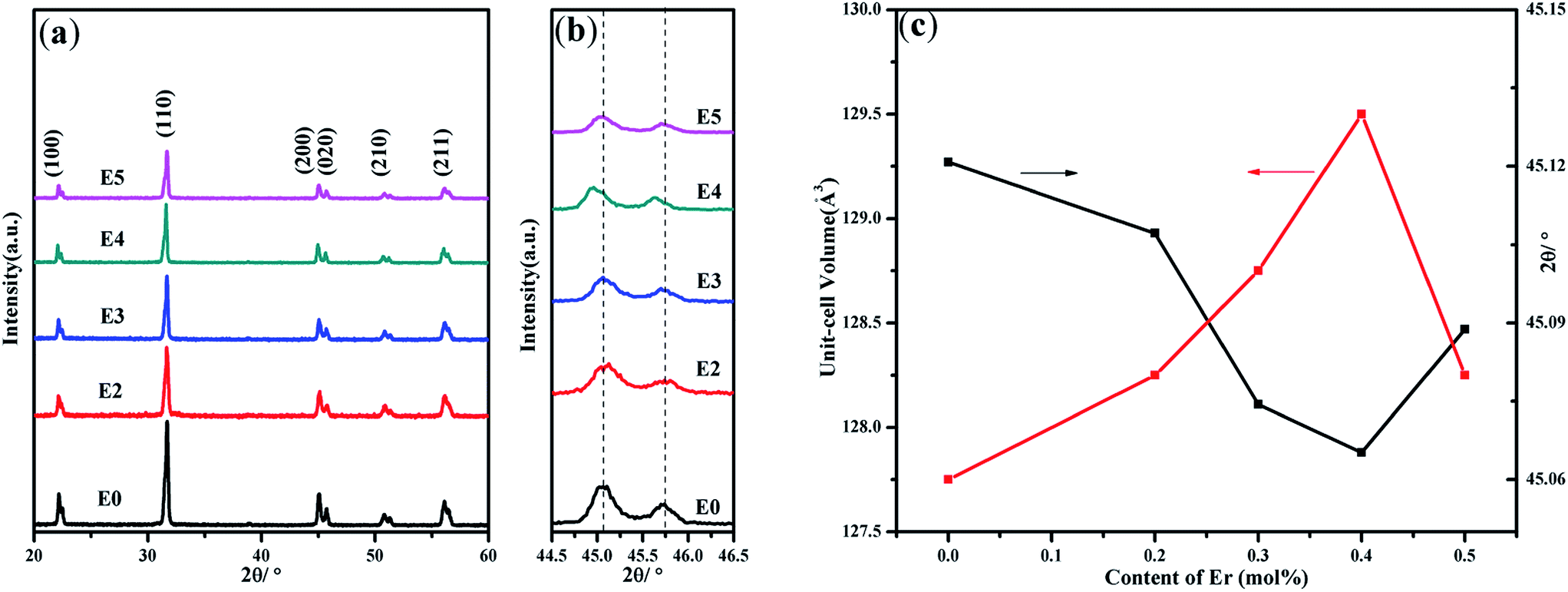 | ||
| Fig. 1 (a) XRD patterns, (b) step scanning of (200) and (020) diffraction peaks, (c) the variation curves for the (200) diffraction peak positions and the as-calculated unit-cell volumes. | ||
To demonstrate the occurrence of lattice distortions, cell-refinement operations were performed based on the XRD results. The variations of the (200) peak positions and as-calculated unit-cell volumes depicted in Fig. 1c showed opposite correlation, evidently supporting the lattice distortions owing to the ions substitution of Er3+ into the KNbO3 lattices. The variation tendency of the lattice constant could be probably caused by the substitution of Er3+ into different sites of ABO3 structure. By considering of the Shannon effective ionic radii (i.e. r(Nb5+, 0.64 Å) < r(Er3+, 0.89 Å) < r(K+, 1.38 Å)), the substitution of Er3+ for K+ (A site) might lead to the shrinkage of the KNbO3 lattice, while the substitution for Nb5+ (B site) might bring about the expansion. The variation of (200) peak positions and unit-cell volumes authentically proved that Er3+ ions firstly occupied the B (Nb5+) site and then A site (K+) as shown in the schematic illustration of Fig. 2.
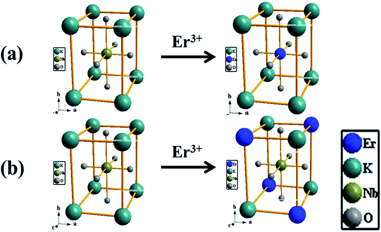 | ||
| Fig. 2 The schematic illustrations for crystal structures of the pure and Er3+doped KNbO3. | ||
The Fig. 3a displayed the Raman spectra at room temperature for KNbO3 with different Er3+ doping contents. Pure KNbO3 with perovskite structure showed a typical Raman spectrum, where the peak of K+ was caused by the vibration of K ions against the NbO6 group (183 cm−1) and ν5 was due to the vibration of the Nb ions against the oxygen octahedron (280 cm−1) at low wavenumbers, while the internal stretching mode of NbO6 was depicted at high wavenumbers. The Raman bonds ν2 and ν1 peaking at 597 and 536 cm−1 represented a double-degenerate symmetric O–Nb–O stretching vibration, which were sensitive to the change of phase structure. The increase in the intensity of ν1 and ν2 for Er3+ doped KNbO3 clearly conformed with the O–Nb–O stretching vibration was affected by the addition of Er3+. Of note, an unexpected phenomenon was observed that three additional peaks at around 450, 730 and 910 cm−1 came into existence when doping content of Er3+ was higher than 0.3 mol%, as marked in the box. To reveal the effect of Er3+ doping on the phase transition of the as-obtained products, the Raman analysis at different temperatures was also carried out. The Raman spectra nearby the transition temperatures were further illustrated in Fig. 3b and c. The conclusion could be easily reached that the transition temperatures were not obviously changed by the incorporation of Er3+.19
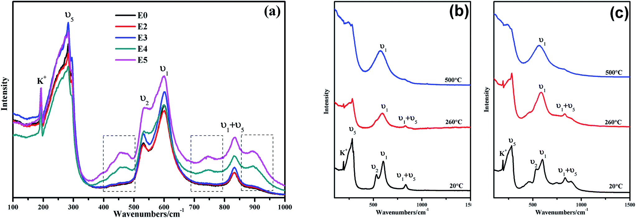 | ||
| Fig. 3 The Raman spectra for: (a) KNbO3 with different Er3+ doping contents, (b) sample E0, (c) sample E4 at different temperatures. | ||
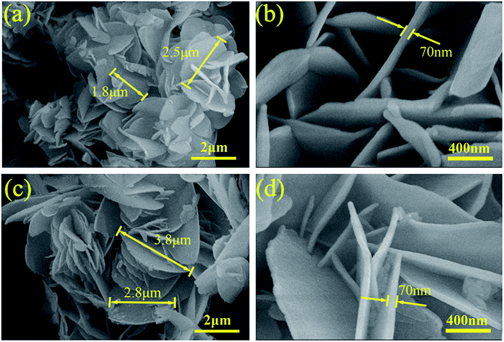
Grain sizes and SEM micrographs were obtained from the pure and Er3+ doped KNbO3 and depicted in Fig. 4. Generally speaking, the morphology of nanosheets for Er3+ doped KNbO3 could be maintained with 0–0.5 mol% of Er3+ doped. Numerous nanosheets flocking together to form hierarchical clusters could be observed as well. The size of pure and 0.4 mol% of Er3+ doped KNbO3 was roughly measured in the SEM images. As shown in Fig. 5, it could be found that the size of the pure and Er3+ doped KNbO3 showed few changes in the thickness. However, the size of Er3+ doped KNbO3 nanosheets became slightly larger in diameter, increasing to 3.5 μm when compared with the size of 2 μm for the pure KNbO3.
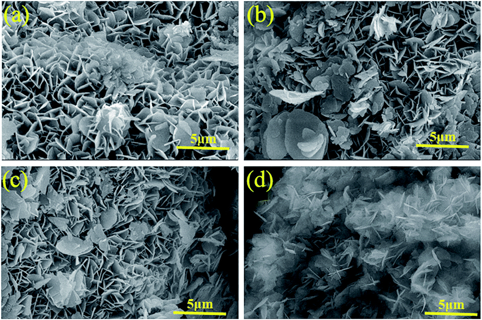 | ||
| Fig. 4 The scanning electron micrographs of KNbO3 with different Er3+ doping contents: (a) 0 mol%, (b) 0.2 mol%, (c) 0.4 mol%, (d) 0.5 mol%. | ||
 | ||
| Fig. 5 The scanning electron micrographs of KNbO3 with different Er3+ doping contents: (a and b) 0 mol%, (c and d) 0.4 mol%. | ||
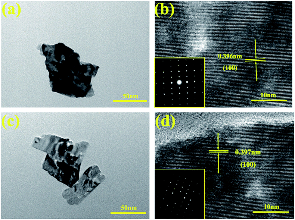
The crystalline states of the pure KNbO3 and 0.4 mol% of Er3+ doped KNbO3 nanosheets were investigated using high-resolution transmission electron microscopy (HRTEM) and the corresponding diffraction patterns were obtained by SAED. The morphology of nanosheet for the as-obtained products could be further confirmed according to Fig. 6a and c. The clear lattice fringe patterns shown in Fig. 6b and d as well as the corresponding diffraction patterns in the insets implied that both of pure and Er3+ doped KNbO3 nanosheets were single crystal. The intervals of the lattice fringes were measured as 0.396 and 0.397 nm according to the diffraction patterns, respectively, which corresponded well with the d spacing value of the (100) plane for orthorhombic KNbO3.
 | ||
| Fig. 6 HRTEM images and diffraction pattern of KNbO3 nanosheets (a and b) 0 mol%, (c and d) 0.4 mol%. | ||
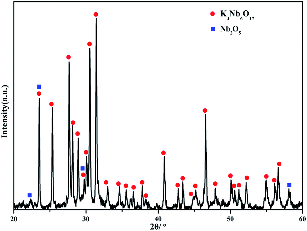
In an attempt to demonstrate the growth process of the Er3+ doped KNbO3 nanosheets, the reactant solution with Er3+ content of 0.4 mol% was treated through the solvothermal method at 200 °C for 4 h, which was less than the general treatment time to obtained the intermediate products. The X-ray diffraction pattern of the intermediate products was performed in Fig. 7. It could be found that the main phase of the intermediate products was K4Nb6O17 while some Nb2O5 remaining owing to the incomplete reaction for 4 h. Hence, the synthesis progresses of the Er3+ doped KNbO3 via a dissolution–precipitation method could be elaborated by the following reactions based on the XRD analysis:
| 3Nb2O5 + 4OH− = Nb6O174− + 2H2O | (1) |
| Nb6O174− + 38OH− = 6NbO67− + 19H2O | (2) |
| 6NbO67− + 6K+ + 3H2O = 6KNbO3 + 36OH− | (3) |
 | ||
| Fig. 7 The X-ray diffraction pattern of the intermediate products with Er3+ content of 0.4 mol% treated through the solvothermal method at 200 °C for 4 h. | ||
Nb6O174− ions was firstly obtained when Nb2O5 dissolved into in the strong alkali environment and then converted into single octahedron NbO67− ions.20 Afterwards, the precipitation of KNbO3 nuclei occurred from the reaction between NbO67− and K+.
The SEM images of the as-obtained intermediate products presented in Fig. 8a–d represented the various morphologies corresponding to different periods, respectively. The size of the nanosheets got enhanced from smaller than 1 μm in Fig. 8a to larger than 5 μm in Fig. 8b. Afterwards, the nanosheets aggregated together to form multilayer structures in Fig. 8c and then the clusters in Fig. 8d. It was worth noting that a lot of nanoparticles with size of ∼50 nm were adhered to the surface of the nanosheets as shown in Fig. 8a–d. The nanoparticles were expected to be the nuclei. Finally, they absolutely grew to the nanosheets thus disappearing after the treatment for 8 h shown in Fig. 4c. The schematic illustrations for the formation of the clusters consisting of nanosheets were further delineated in Fig. 8e based on Fig. 8a–d. As depicted in Fig. 8e, the nuclei were firstly formed due to the dissolution and precipitation process. Afterwards, they were inclined to grow along specific directions to form nanosheets as depicted in step 1. As a result, the integrated nanosheets were formed through the Ostwald ripening process.21 Meanwhile, the nanosheets aggregated into multilayer structures in step 2 and finally clusters in step 3.
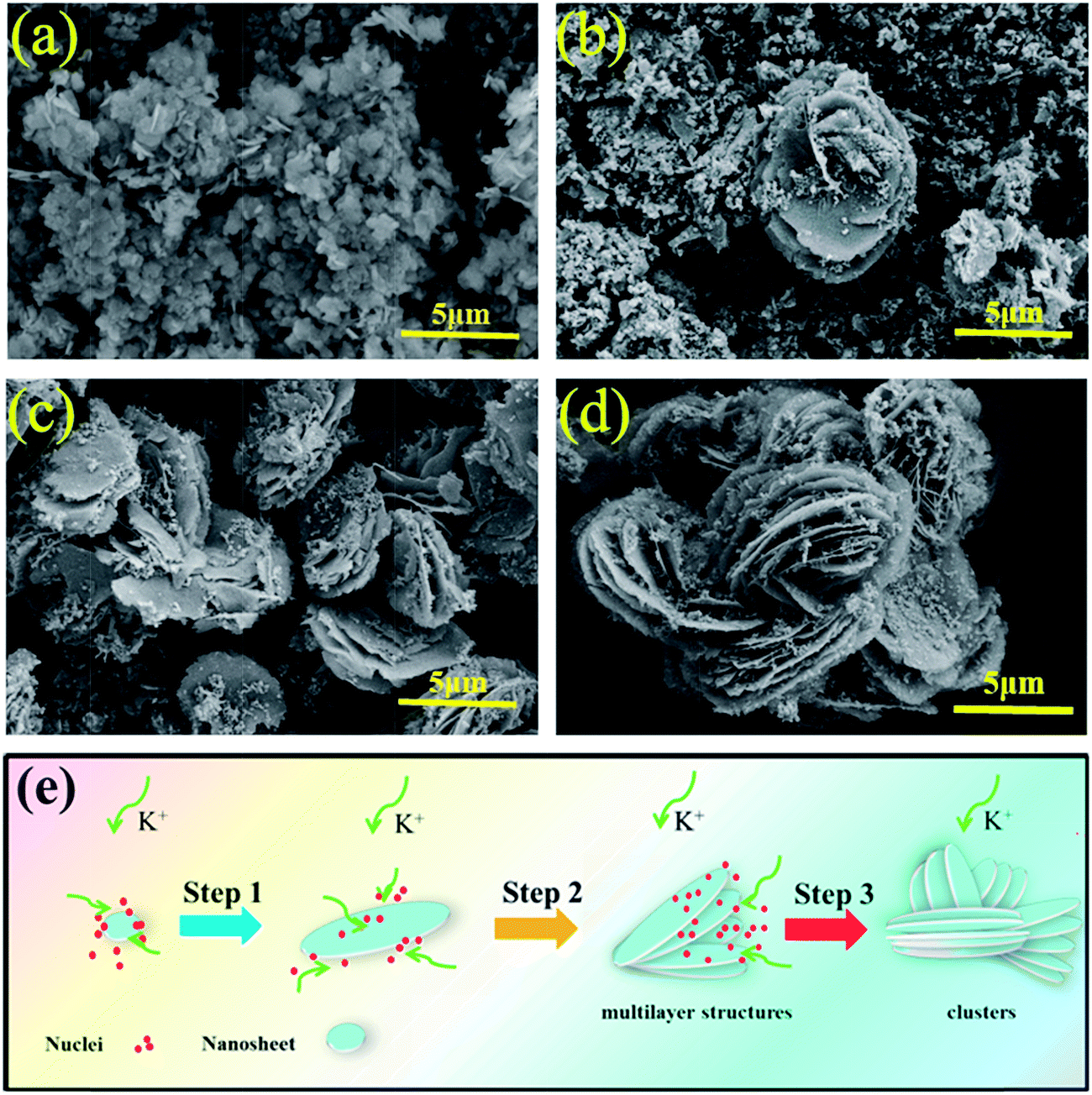 | ||
| Fig. 8 The SEM images of KNbO3 nanosheets with Er3+ content of 0.4 mol% treated through the solvothermal method at 200 °C for 4 h (a–d), (e) the schematic illustrations for the formation of Er3+ doped KNbO3 nanosheets. | ||
In the solvothermal reaction, the high viscosity of EG solution played a significant role in tailoring the growth and the morphology of the KNbO3 nanosheets in two aspects. Firstly, super-saturation and nucleation were accelerated by EG due to the low activity coefficient and outstanding solubility to precursors.22,23 Secondly, the size of KNbO3 was controlled by EG by reducing the diffusive rates of ions and matching the mass transportation rates of different ions thus hindering growth.24
The up-conversion photoluminescence (UC PL) emission spectra of the Er3+ doped KNbO3 were shown in Fig. 9a. The pure KNbO3 did not exhibit up-conversion luminescence property, while green and red emission bands were clearly observed for Er3+ doped KNbO3 as expected.25,26 The strong green emission (520–580 nm) was corresponding to the transition of 2H11/2 and 4S3/2 to 4I15/2 and the weak red emission (625–700 nm) was attributed to the transition of 4F9/2 to 4I15/2. Both of the integrated green and red emission intensities were enhanced until the contents of Er3+ reached 0.4 mol% due to the sensitization effects and then decreased with further increasing of Er3+ as depicted in Fig. 9b. This decrement could be ascribed to the content-quenching effect of Er3+.27 The quenching effect was mainly caused by the promotion of energy transfer among Er3+ ions when the distance among Er3+ ions got shorter with higher contents. The ratio of emission intensity Igreen/Ired with different contents of Er3+ was also delineated in Fig. 9b. The value of the intensity ratio was increased with the Er3+ doping content, indicating that the transition of 2H11/2 and 4S3/2 to 4I15/2 was more sensitive to the doping contents of Er3+. In other words, the ratio of green and red emission intensity regulation could be easily achieved by the addition of Er3+.
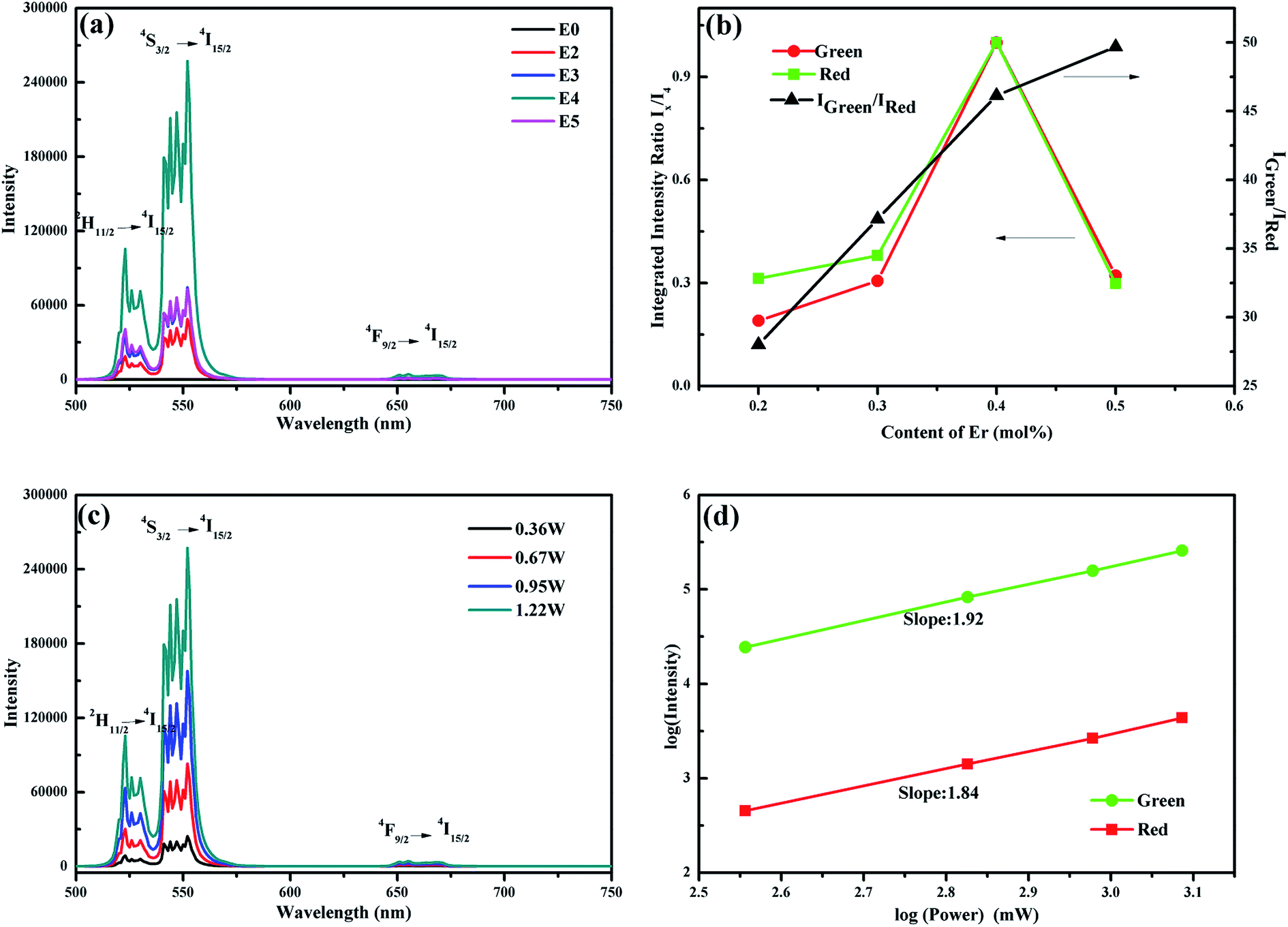 | ||
| Fig. 9 (a) The UC PL spectra and (b) the variation of green and red emission intensities for KNbO3 with different contents of Er3+ doped, (c) the UC PL spectra for E4 under different laser input powers, (d) the emission intensities log–log plotted against the excitation powers for sample E4. | ||
In order to explore the mechanism of the UC PL properties for the Er3+ doped KNbO3, the UC PL spectra under various laser input powers for the sample E4 were displayed in Fig. 9c, and the variation curves of emission intensities against the excitation powers were further depicted in Fig. 9d. It had been reported that the emission intensity was proportional to the mth power of excitation power, where m is the number of the absorbed photons.28
In this work, the obtained values of the slopes were 1.92 and 1.84 for the green and red emission, respectively, implying that two photons contributed to the up-conversion luminescence property. On the basis of aforementioned discussions, the KNbO3 with 0.4 mol% of Er3+ doped exhibited the optimal UC PL properties while maintaining the structure and the morphology of the pure KNbO3, showing great potential as a candidate for multifunctional devices.
Conclusions
The Er3+ doped single crystal KNbO3 nanosheets with the thickness of about 70 nm and the diameter of 3 μm were prepared via a solvothermal method. The XRD analysis demonstrated that Er3+ firstly occupied B site in perovskite structure of KNbO3 and then A site with the increasing content of Er3+. The Raman shift reconfirmed that Er3+ ions were successfully doped into the KNbO3 host. The single crystal structure of the as-obtained KNbO3 was certified by the HRTEM and the corresponding diffraction patterns. The growth mechanism of the KNbO3 nanosheets was elaborated. The most outstanding UC PL property of strong green emission and weak red emission was endowed to the KNbO3 nanosheets by the doping of 0.4 mol% Er3+. It was confirmed that two photons contributed to this UC PL behaviors based on the spectra exited by different laser power. As a conclusion, the as-synthesized perovskite KNbO3 nanosheets with excellent UC PL property could be the potential alternative materials for the development of multifunctional devices.Acknowledgements
This work was supported by the National Nature Science Foundation of China (No. 51272119 and 51302145), Beijing Institute of Technology Research Fund Program for Young Scholars, and the State Key Laboratory of New Ceramics and Fine Processing of Tsinghua University.References
- W. Sark, A. Meijerink and R. E. I. Schropp, Sol. Energy Mater. Sol. Cells, 2005, 87, 395 CrossRef
.
- F. Li, D. Liu, G. Gao, B. Xue and Y. Jiang, Appl. Catal., B, 2015, 166, 104–111 CrossRef
- P. Kang, T. Lee, C. Ahn, I. Kim, H. Lee, S. Choi, K. Sung and J. Jung, Nano Energy, 2015, 17, 261–268 CrossRef CAS
- C. Wen, S. Chu, S. Tyan and Y. Juang, J. Cryst. Growth, 2004, 262, 225–230 CrossRef CAS
- A. Gomes, S. Lima, I. Eguiluz and R. Salazar-Banda, J. Mater. Sci., 2016, 51, 4709–4727 CrossRef
- S. Wang, H. Zhou, X. Wang and A. Pan, J. Phys. Chem. Solids, 2016, 98, 28–31 CrossRef CAS
- C. Araujo, L. Menezes, G. Maciel, L. Acioli, A. Gomes, Y. Messaddeq, A. Florez and M. Aegerter, Appl. Phys. Lett., 1996, 68, 602 CrossRef
- X. Wu, K. Kwok and F. Li, J. Alloys Compd., 2013, 580, 88–92 CrossRef CAS
- B. Dong, B. Cao, Y. He, Z. Liu, Z. Li and Z. Feng, Adv. Mater., 2012, 24, 1987 CrossRef CAS PubMed
- Y. Zhao, Y. Ge, X. Zhang and Y. Zhao, J. Alloys Compd., 2016, 680, 467–472 CrossRef CAS
- Y. Ge, Y. Zhao, X. Yuan, S. Sun, Y. Zhao and H. Zhou, RSC Adv., 2016, 6, 67353–67360 RSC
- Y. Zhao, Y. Ge, X. Yuan and Y. Zhao, J. Alloys Compd., 2016, 683, 171–177 CrossRef CAS
- Y. Wang, L. Wang, Y. Zhao and D. Yan, Ceram. Int., 2016, 42, 17911–17915 CrossRef CAS
- X. Wu, T. Chung and K. Kwok, Ceram. Int., 2015, 41, 14041–14048 CrossRef CAS
- Y. Wang, Z. Chen, Z. Ye and J. Huang, J. Cryst. Growth, 2012, 341, 42–45 CrossRef CAS
- R. Wang, Y. Zhu, Y. Qiu and C. Leung, Chem. Eng. J., 2013, 226, 123–130 CrossRef CAS
- Y. Wang, L. Wang, Y. Zhao and X. Yuan, Mater. Lett., 2016, 179, 210–213 CrossRef CAS
- I. Krad, O. Bidault, S. Said and M. Maaoui, Mater. Lett., 2015, 159, 237–240 CrossRef CAS
- C. Wen, S. Chu, Y. Juang and C. Wen, J. Cryst. Growth, 2005, 280, 179–184 CrossRef CAS
- K. Goh and F. Lange, J. Mater. Res., 2003, 18, 338–345 CrossRef
- F. Madaro, J. Tolchard and Y. Yu, CrystEngComm, 2011, 13, 1350–1359 RSC
- G. Xu, X. Huang, Y. Zhang, S. Deng, X. Wei and G. Shen, CrystEngComm, 2013, 15, 7206 RSC
- H. Ghafarian, M. Javanbakht and M. Ghaemi, J. Power Sources, 2015, 284, 339–348 CrossRef
- G. Xu, F. Li, Z. Tao, X. Wei, Y. Liu, X. Li, Z. Ren and G. Shen, J. Power Sources, 2014, 246, 696–702 CrossRef CAS
- J. Wu, Z. Wu, W. Qian, Y. Jia, Y. Wang and H. Luo, Mater. Lett., 2016, 184, 131–133 CrossRef CAS
- S. Gong, M. Li, Z. Ren, X. Yang, X. Li, G. Shen and G. Han, J. Phys. Chem. C, 2015, 119, 17326–17333 CAS
- R. Xie, N. Hirosaki, K. Sakuma, Y. Yamamoto and M. Mitomo, Appl. Phys. Lett., 2004, 84, 5404–5406 CrossRef CAS
- A. Shalav, B. Richards, T. Trupke, K. Krämer and H. Güdel, Appl. Phys. Lett., 2005, 86, 013505 CrossRef
Footnote |
| † These authors contributed equally to this work. |
| This journal is © The Royal Society of Chemistry 2016 |