DOI:
10.1039/C6RA22423G
(Paper)
RSC Adv., 2016,
6, 106374-106379
Enhancement of reliability and stability for transparent amorphous indium-zinc-tin-oxide thin film transistors
Received
7th September 2016
, Accepted 3rd November 2016
First published on 3rd November 2016
Abstract
We studied the influence of the backchannel passivation layer (BPL) on the ambient stability of amorphous indium-zinc-tin-oxide thin-film transistors (a-IZTO TFTs), in which atomic layer deposited (ALD) Al2O3 films and plasma-enhanced chemical vapor deposited (PECVD) SiO2 films were separately used to be the channel passivation layers. It was observed that the BPL deposition process strongly affects device performance and stability. From the results of the extracted activation energy (Eact), the Al2O3 passivation layer can reduce the trap density in localized tail states, which improves the mobility of a-IZTO TFTs. Compared with the SiO2 passivation layer, the Al2O3 passivation process effectively suppresses H injection into the a-IZTO channel layer underneath with secondary ion mass spectrometer analysis. In addition, it is found that the a-IZTO TFT with the Al2O3 passivation layer can enhance resistance against negative bias illumination stress (NBIS), making it reliable for realistic operation in flat panel displays.
1. Introduction
Recently, amorphous indium zinc tin oxide (a-IZTO) has attracted a lot of attention, competing with amorphous indium gallium zinc oxide (a-IGZO) as the channel layer material in thin film transistors (TFTs) for next generation flat-panel displays. According to its material characteristics, a higher carrier mobility can be obtained due to the better conductive path for electrons produced by replacing the tin cation with a gallium cation. According to previous studies, oxide TFTs including a-IGZO TFTs are sensitive to oxygen and moisture during the bias stability test, resulting in threshold voltage shift.1 For example, the oxygen species absorbed from the ambient atmosphere can capture electrons in the metal oxide based active layer to generate negatively charged species, as follows:where e− denotes electrons, and O2(g) and O2(s)− represent the neutral and charged oxygen molecules in the back channel of a-IGZO TFTs. While the negative space charges O2(s)− generate, the positively shift of threshold voltage can be observed. Hence, the backchannel passivation layer (BPL) for oxide TFTs is necessary to suppress environmental factors. Besides, the materials and BPL deposition processes are another important topics and should be optimized for oxide TFTs technology. Choi et al. reported that silicon dioxide (SiO2) and silicon nitride (SiNx) deposited by plasma-enhanced chemical vapor deposition (PECVD) may cause the degradation of a-IGZO TFTs due to plasma-induced radiation damage at the back channel surface. In this case, the TFT devices perform lower mobility and larger hysteresis window.2 In addition, the remaining of the hydrogen from the incompletely dissociated precursor may diffuse into the a-IGZO channel as the shallow donor states resulting in the conducting electrical performance or thermal instability of TFT devices.3,4 However, even though there are some literatures showed that the a-IZTO TFTs could deposit at room temperature and exhibit good electrical performance and reliability, the study on environment stability is still lacking.5 The influence of passivation layer on this high carrier concentration material of IZTO thin film is unclear.
In the present work, the effect of backchannel passivation layer on a-IZTO TFT has been well discussed. The SiO2 and Al2O3 passivation layers were fabricated by PECVD and plasma-enhanced atomic layer deposition (PE-ALD), respectively. The electrical characteristic of a-IZTO TFTs with BPL have been optimized through adjusting process parameters such as reaction precursors, gas flow rate and deposition temperatures. From secondary ion mass spectrometer (SIMS) analysis, the proposed mechanism of device performance degradation for the passivated a-IZTO TFT can be confirmed. In addition, the environment stability and bias reliability of passivated a-IZTO TFTs have also been well discussed with the corresponding mechanism.
2. Experiment
The inverted-staggered a-IZTO TFT devices with passivation layer were fabricated for this study with following procedures.
For the first step, a 100 nm-thick thermal oxide as the gate insulator layer was firstly grown on the n+ heavily doped silicon substrates by a horizontal thermal furnace after a RCA clean process. Then, the 30 nm-thick a-IZTO channel layers were deposited by using RF magnetron sputtering at 70 W using IZTO target of In![[thin space (1/6-em)]](https://www.rsc.org/images/entities/char_2009.gif) :Sn:Zn:O = 4:4:1:15 at%. The sputtering process pressure was carried out at 3 mTorr with the argon and oxygen flow rate of 10 sccm and 0.1 sccm, respectively. The source and drain electrodes of 100 nm-thick ITO were formed by RF magnetron sputtering at 50 W in argon atmosphere with a flow rate of 10 sccm. The process pressure was also carried out at 3 mTorr. After the fabrication of bottom gate a-IZTO TFTs, the SiO2 or Al2O3 thin films were sequentially capped on the devices to act as the passivation layer. The 50 nm-thick SiO2 passivation layers were deposited by PECVD at 25 W with silane (SiH4) and nitrous oxide (N2O) flow rate of 9 sccm and 710 sccm, respectively. The pressure and temperature was fixed at 1000 mTorr and 300 °C. In order to reduce the remaining hydrogen in SiO2 layers, another deposition condition was adopted with the mixture precursor of tetraethyl orthosilicate (TEOS) and oxygen (O2), where the gas flow rate was fixed at 50 sccm and 300 sccm, respectively. For better TEOS dissociation, the process temperature was raised to 350 °C with a power of 40 W. The 15 nm-thick Al2O3 passivation layers were deposited under the plasma environment composed of trimethylaluminum (TMA) and O2 by ALD process at 250 °C. The reaction pressure was carried out at 10 mTorr. The via to the source/drain electrodes were patterned and then etched by high density plasma reactive etching (HDPRIE) with mixture gases of Ar/CF4 for SiO2 and Ar/BCl3/Cl2 for Al2O3. Fig. 1 illustrates the cross-sectional schematic diagrams of the fabricated a-IZTO devices. Finally, all of devices were thermally annealed under the oxygen atmosphere with flow rate of 80 sccm at several temperatures for an hour. Both the channel width and length of devices were varied from 1000 to 200 μm. The electrical properties were measured using Keithley SCS 4200 semiconductor parameter analyzer in the dark chamber at room temperature. In addition, the 30 nm-thick a-IZTO thin films capped by the passivation layers were deposited on the SiO2/Si substrate with different annealing conditions to analyze the chemical composition by secondary ion mass spectrometer (SIMS).
:Sn:Zn:O = 4:4:1:15 at%. The sputtering process pressure was carried out at 3 mTorr with the argon and oxygen flow rate of 10 sccm and 0.1 sccm, respectively. The source and drain electrodes of 100 nm-thick ITO were formed by RF magnetron sputtering at 50 W in argon atmosphere with a flow rate of 10 sccm. The process pressure was also carried out at 3 mTorr. After the fabrication of bottom gate a-IZTO TFTs, the SiO2 or Al2O3 thin films were sequentially capped on the devices to act as the passivation layer. The 50 nm-thick SiO2 passivation layers were deposited by PECVD at 25 W with silane (SiH4) and nitrous oxide (N2O) flow rate of 9 sccm and 710 sccm, respectively. The pressure and temperature was fixed at 1000 mTorr and 300 °C. In order to reduce the remaining hydrogen in SiO2 layers, another deposition condition was adopted with the mixture precursor of tetraethyl orthosilicate (TEOS) and oxygen (O2), where the gas flow rate was fixed at 50 sccm and 300 sccm, respectively. For better TEOS dissociation, the process temperature was raised to 350 °C with a power of 40 W. The 15 nm-thick Al2O3 passivation layers were deposited under the plasma environment composed of trimethylaluminum (TMA) and O2 by ALD process at 250 °C. The reaction pressure was carried out at 10 mTorr. The via to the source/drain electrodes were patterned and then etched by high density plasma reactive etching (HDPRIE) with mixture gases of Ar/CF4 for SiO2 and Ar/BCl3/Cl2 for Al2O3. Fig. 1 illustrates the cross-sectional schematic diagrams of the fabricated a-IZTO devices. Finally, all of devices were thermally annealed under the oxygen atmosphere with flow rate of 80 sccm at several temperatures for an hour. Both the channel width and length of devices were varied from 1000 to 200 μm. The electrical properties were measured using Keithley SCS 4200 semiconductor parameter analyzer in the dark chamber at room temperature. In addition, the 30 nm-thick a-IZTO thin films capped by the passivation layers were deposited on the SiO2/Si substrate with different annealing conditions to analyze the chemical composition by secondary ion mass spectrometer (SIMS).
 |
| | Fig. 1 Schematic structure of a-IZTO TFT device with backchannel passivation layer. | |
3. Results and discussion
To compare the backchannel passivation effects on the a-IZTO TFTs, the transfer characteristic (ID–VG curve) of TFT devices with different kinds of BPL processes are shown in Fig. 2. The electrical parameters extracted from each device are shown in Table 1. The black and white circle symbol shows the performance of the a-IZTO TFT without BPL annealed at 300 °C and 400 °C for 30 min, respectively. In our previous study,6 the higher annealing temperature can improves both electrical characteristic and reliability of devices, however, leading to a significant Vth shift negatively. This issue can be released in the BPL a-IZTO TFT devices with a more positive Vth around 0 V.
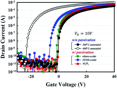 |
| | Fig. 2 Transfer characteristics of the a-IZTO TFTs with different types of passivation layers for comparison. The curve with black and white symbol shows the un-passivated a-IZTO TFTs after annealing process at 300 °C and 400 °C, respectively. | |
Table 1 Summary of the electrical parameters extracted from a-IZTO TFT devices with and without backchannel passivation layers
| Optimized condition |
Vth (V) |
Mobility (cm2 V−1 s−1) |
s.s. (V per decade) |
| Passivation free (300 °C) |
−0.72 |
20.46 |
0.32 |
| Passivation free (400 °C) |
−22.76 |
37.9 |
0.40 |
| Silane SiO2 |
−1.92 |
27.51 |
0.41 |
| TEOS SiO2 |
−6.48 |
27.09 |
0.51 |
| ALD Al2O3 |
−0.88 |
30.16 |
0.34 |
The BPL thin film, including SiO2 or Al2O3, can play a role to prevent weakly bonding oxygen from desorbing out to the environment from a-IZTO channel during annealing. Among these devices with BPL, the Al2O3-passivated a-IZTO TFTs perform the superior electrical characteristics with mobility of 30.16 cm2 V−1 s−1 and subthreshold slope (s.s.) of 0.34 V per decade. This result can be attributed to the reduction of local tail states in a-IZTO channel layer from around 1018 eV−1 cm−3 to around 1017 eV−1 cm−3, extracted from ID–VG curve at various measurement temperatures. In addition, the ID–VG curve is nearly overlapped with that of the one without BPL annealed at 300 °C with the similar Vth of −0.88 V, which indicates the ALD process provides the radiation-free damage without forming oxygen vacancies at the back a-IZTO channel. On the other hand, the effect of ion bombardment from PECVD process makes the Vth shifted to a negative value, especially significant for the case of TEOS-SiO2 BPL. The cause of obvious negative shift can be excluded from the hydrogen incorporation due to the fewer residual hydrogen contained in the TEOS-SiO2 process.
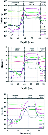
Fig. 3(a)–(c) show the transfer characteristic of a-IZTO TFTs with BPL measured at 25 °C, 50 °C, 70 °C and 90 °C. The Vth value shifts negatively and the off-current (Ioff) increases with increasing measurement temperatures from 25 °C to 90 °C. This phenomenon can be described by the thermally activated Arrhenius model, where it is assumed that thermally activated electrons from deep level trap sites into the conduction band move quickly toward the drain electrode due to a lateral electrical field.7 The drain current (ID) is activated thermally and described as following equation:8
| |
 | (2) |
where the
IO is the pre-factor,
k is the Boltzmann constant,
T is the absolute temperature K,
Eact is the activated energy which is defined as
Eact =
Ec −
EF. The conductance activation energy (
Eact) calculated from the Arrhenius plot is used to approximately track the position of Fermi level (
Eact =
Ec −
EF) in the energy band gap,
9 where
Ec and
EF are defined as conduction band edge and Fermi energy, respectively. Therefore, the activation energy can be determined from the curve of ln(
ID)
versus reciprocal of temperature (1/
T) by measuring the drain–source current at different temperature with the same drain–source voltage, the activation energy can be extracted with the following equation:
| |
 | (3) |
 |
| | Fig. 3 Temperature-dependent transfer characteristics of a-IZTO TFT with (a) silane-SiO2-passivated backchannel layer, (b) TEOS-SiO2-passivated backchannel layer, and (c) ALD-Al2O3-passivated backchannel layer. (d) The plot of activated energy (Eact) versus gate voltage (VG) for a-IZTO TFTs with different types of backchannel passivation layers. | |
For TFT operation, most of the charge induced by the gate voltage goes into the tail states with a small fraction going into the conduction band, and the EF moves closer to the edge of the conduction band with increasing gate voltage. Hence, the ease of the EF movement is determined by the distribution of the tail states. The faster moving EF with gate voltage means total trap density is lower due to less shallow trap in tail states.10 The Eact versus gate voltage of passivated a-IZTO TFTs is shown in Fig. 3(d). Table 2 shows the slope of Eact change versus VG. The average declined slopes of Eact for Al2O3-passivated a-IZTO TFTs is steeper than others, in other words, EF can approach Ec easily due to the lower shallow trap in tail states indicated that a-IZTO thin film with Al2O3 passivation layer can reduced the trap density more than others. Furthermore, the bias and temperature dependence on the leakage current was observed in a-IZTO TFTs with PECVD-processed BPL. In general, the leakage conduction paths in the bottom-gate TFT devices are formed at the front and backchannel layers, respectively, shown in Fig. 4(a). The conduction path occurred at the front channel can be attributed to the Poole–Frenkel leakage current through the accumulated holes with high negative VG bias and high positive VD bias as shown in the path 1 in Fig. 4(a). The holes are generated at the gate–drain overlap region by Poole–Frenkel field enhanced thermionic emission.11 From previous literatures, however, the amount of the hole carriers in oxide semiconductors is negligible due to the atomic configuration and electronic structure.12 This indicates the path 1 might not be the leakage path in this study. We speculate the conduction path for the leakage current to be from the back channel with large defect states, as shown in the path 2 of Fig. 4(a). In the plasma-related BPL process, a lot of subgap states are easily formed at backchannel layer due to the ion bombardment effect and resultantly trapping electrons which could be thermally excited to the conduction band and hopping to the drain electrode, as shown in Fig. 4(b). With higher measuring temperature, the more thermal electrons could be generated thermally and conductive along the path 2. Especially, a higher electric field across the gate–drain overlap region will even enhance the leakage conduction, as the negative VG bias increased and raised up the potential energy of a-IZTO layer, as shown in Fig. 4(c).
Table 2 The value of slope Eact versus VG for a-IZTO TFT devices with backchannel passivation layers
| Passivation type |
Silane-SiO2 |
TEOS-SiO2 |
Al2O3 |
| Slope (|ΔEa|/|Δvoltage|) |
0.29 |
0.25 |
0.38 |
 |
| | Fig. 4 (a) The schematic mechanism for leakage current of a-IZTO TFT with backchannel passivation layer at turn-off region. (b) Energy band diagram of leakage conduction for temperature-dependent. (c) Bias-dependent behavior. | |
The bias reliability test of the a-IZTO TFTs with BPL was also conducted in this study. Fig. 5(a)–(f) show the transfer characteristic of a-IZTO TFT devices with BPL under positive gate bias stress (PGBS) and negative gate bias stress (NGBS), respectively. The device parameters including the mobility and s.s. all perform a similar value after bias reliability test, indicating no additional defect states created. The Vth shift is shown in Fig. 6. In this measurement, an electric field of ±2.5 MV cm−1 was applied to gate electrode and source/drain electrodes were grounded for 2000 s at ambient environment.
 |
| | Fig. 5 Transfer characteristics of a-IZTO TFT with (a) silane-SiO2-passivated backchannel passivation layer, (b) TEOS-SiO2-passivated and backchannel passivation layer (c) Al2O3-passivated backchannel passivation layer under positive gate bias stress (PGBS). Transfer characteristics of a-IZTO TFT with (d) silane-SiO2-passivated backchannel passivation layer, (e) TEOS-SiO2-passivated and backchannel passivation layer (f) Al2O3-passivated backchannel passivation layer under negative gate bias stress (NGBS). | |
 |
| | Fig. 6 Vth shift of a-IZTO TFTs with backchannel passivation layers as a function of gate bias stress durations for (a) PGBS test and (b) NGBS. | |
The gate bias stress measurement results for the passivation-free sample were under the atmosphere ambient and vacuum environment, while all TFT devices with passivation layers were measured under atmosphere ambient environment. It is clearly observed that the Vth shift of the a-IZTO TFTs with BPL was smaller than the one without BPL with 2.84 Vth shift. These results indicated that the BPL can effectively isolate the influences from the ambient. When the positive gate bias stress was applied, the absorption of oxygen species from ambient atmosphere occurs and then captures electrons in the a-IZTO channel layer to form negative charges, described by eqn (1). The additional generation of negative space charges will result in the positive Vth shift. On the contrary, the effect of moisture absorption dominates the NBGS behavior by releasing electron and then forming positive space charges (H2O+) as well as leading to a negative Vth shift. In PGBS test, the Vth shift of a-IZTO TFT without BPL measured in vacuum is slightly smaller than that in ambient, indicating that the absorption of oxygen molecules from the atmosphere is certainly reduced in vacuum. Also, in Al2O3-passivated a-IZTO TFTs the O2(s)− species can also be isolated effectively by the backchannel passivation layer with a much smaller Vth shift of 1.12 V. The similar result is also observed in NGBS test. The passivation layer can also prevent the influence of moisture in the environment from shifting the Vth to a negative value. We believe that the IZTO device with TEOS SiO2 suffered from a certain extent water vapor absorption from the ambient environment. In other words, the TEOS SiO2 compared with silane SiO2 is not suitable to be the passivation layer of IZTO TFTs to isolate the moisture from the ambient. As a result, the passivation-free sample stressed under the vacuum need not to have the biggest threshold voltage shift under negative bias stress because the moisture absorption in vacuum hardly occurs. However, under PGBS, the slightly negative Vth shift is observed for the SiO2-passivated a-IZTO TFTs by PECVD process. This negative Vth shift of SiO2-passivated TFT devices may be attributed to the hydrogen diffusion into the a-IZTO channel and explained by following equation:12
where H
0 is the neutral hydrogen atom from the PECVD process environment. The SiO
2 passivation layer tends to combine with oxygen atom in the a-IZTO channel to release a free carrier because of the stronger O–H bonds. During PGBS, the hydrogen incorporation at the back channel and reduce the energy difference between
EF and
Ec. In addition, the
EF is subjected to be pinned due to the interface states within the a-IZTO and this energy bands are modified due to the Fermi level pinning not being recovered even when the PBGS is terminated.
13 This phenomenon can be ignored in the Al
2O
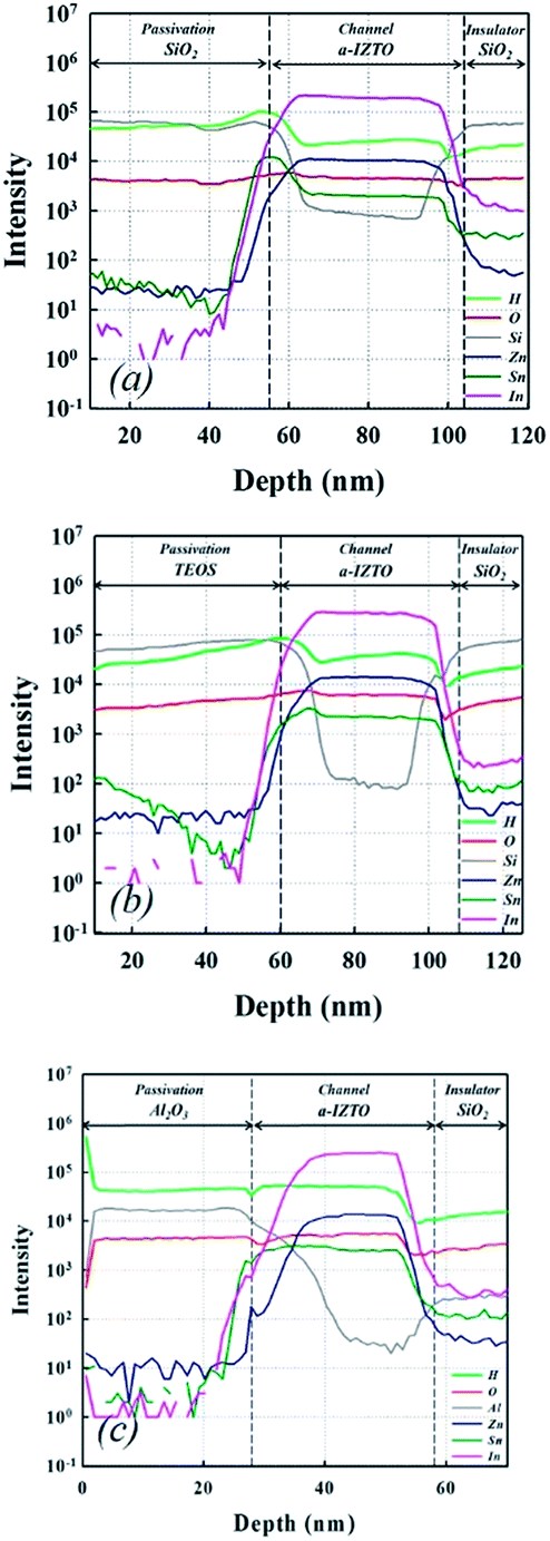
3-passivated a-IZTO TFTs with fewer hydrogen diffusions from passivation layer. SIMS analysis can be performed to confirm the proposal, as shown in
Fig. 7. It is observed that the signal intensity of hydrogen in the SiO
2-passivated TFT sample is half order of magnitude higher than that in Al
2O
3-passivated sample at the interface between a-IZTO channel and the passivation layer.
 |
| | Fig. 7 SIMS depth profiles of a-IZTO films capped by (a) silane-SiO2 thin film, (b) TEOS-SiO2 thin film, and (c) Al2O3 thin films on Si substrate. | |
The negative bias illumination stress (NBIS) of a-IZTO TFTs with BPL is also further studied. A gate bias stresses of −25 V and blue light (λ = 465 nm) at a power density of 0.2 mW cm−2 were applied to TFT devices in the NBIS testing. Fig. 8 shows the Vth shift of a-IZTO TFTs versus stress time during the NBIS test. It is found the Vth shift of TFT devices under NBIS is much larger than NBS. The electrical degradation mechanism is related to high density of oxygen deficiencies (VO) corresponded to the deep level states located near the VBM. These defect states can be photo-excited to the ionized oxygen deficiencies ( ,
,  ) and accumulated to the interface by gate electrical field.14 Another mechanism for NBIS degradation is about the photo-desorption of oxygen species at the surface of channel layer.15 Under the light illumination, the oxygen species donates the free electron in the conduction band, which enhances the conductivity. It is obviously that the passivated a-IZTO TFTs have a superior NBIS reliability with less than 10 V of negative Vth shift compared to the un-passivated devices, which indicates the deep level defect states of channel can be eliminated by backchannel passivation process. As for the sample of Al2O3-passivated a-IZTO TFT, O2 plasma during the passivation layer deposition re-oxidizes the a-IZTO channel layer and reduces the oxygen deficiencies. In addition, the Al2O3 passivation layer could effectively isolate the oxygen absorption on the a-IZTO surface and prevent photo-desorption behavior. Therefore, a-IZTO TFT with Al2O3 shows the most stable electrical characteristics than others. This can be inferred the ALD method can provide a damage-free process avoiding the ion bombardment during film deposition and maintains the in-diffusion of radical oxygen species into the back surface region of the IZTO channel.16
 |
| | Fig. 8 The Vth shifts versus stress time of a-IZTO TFTs with backchannel layers under NBIS test. | |
4. Conclusions
The characteristics of a-IZTO TFTs with passivation layers have been studied in this work. The electrical degradation of TFT devices after using PECVD SiO2 as passivation layer is dominated by oxygen vacancy near the back channel interface, which is created by ion bombardment effect. Besides, PECVD SiO2 process will cause hydrogen incorporation into a-IZTO channel layer and results in the negative threshold voltage shift under gate bias stressing test. The a-IZTO TFT with PE-ALD Al2O3 passivation layer can prevent from effects of ion bombardment and hydrogen diffusion to the backchannel interface. From the results of extracted activation energy (Eact), the Al2O3 passivation layers can effectively reduce the trap density in localized tail states, which enhanced the mobility of a-IZTO TFTs. Furthermore, ambient stability and electrical reliability under light illumination can be thereby enhanced.
Acknowledgements
The authors would like to thank the Ministry of Science and Technology of the Republic of China, Taiwan for financially supporting this research under Contract No. MOST 103-2221-E-009-010-MY3. Also, this work was performed at National Nano Device Laboratories, Taiwan, R.O.C.
Notes and references
- J. S. Park, J. K. Jeong, H.-J. Chung, Y. G. Mo and H. D. Kim, Appl. Phys. Lett., 2008, 92, 072104 CrossRef.
- S. H. Choi, J. H. Jang, J. J. Kim and M. K. Han, Electron Device Lett., 2012, 33, 381 CrossRef CAS.
- H. Godo, D. Kawae, S. Yoshitomi, T. Sasaki, S. Ito, H. Ohara, H. Kishida, M. Takahashi, A. Miyanaga and S. Yamazaki, Jpn. J. Appl. Phys., 2010, 49, 03CB04 CrossRef.
- C. Y. Lin, C. W. Chien, C.-H. Wu, H. H. Hsieh, C.-C. Wu, Y. H. Yeh, C.-C. Cheng, C.-M. Lai and M.-J. Yu, IEEE Trans. Electron Devices, 2012, 59, 1701 CrossRef CAS.
- J. H. Song, K. S. Kim, Y. G. Mo, R. Choi and J. K. Jeong, Electron Device Lett., 2014, 35, 853 CrossRef CAS.
- C. S. Fuh, P. T. Liu, W. H. Huang and S. M. Sze, Electron Device Lett., 2014, 35, 1103 CrossRef CAS.
- K. Hwan Ji, J. I. Kim, H. Y. Jung, S. Y. Park, Y.-G. Mo, J. H. Jeong, J.-Y. Kwon, M. K. Ryu, S. Y. Lee, R. Choi and J. K. Jeong, J. Electrochem. Soc., 2010, 157, H983 CrossRef.
- A. Sato, K. Abe, R. Hayashi, H. Kumomi, K. Nomura, T. Kamiya, M. Hirano and H. Hosono, Appl. Phys. Lett., 2009, 94, 133502 CrossRef.
- C. T. Tsai, P. T. Liu, T. C. Chang, C. W. Wang, P. Y. Yang and F. S. Yeh, Electron Device Lett., 2007, 28, 584 CrossRef CAS.
- K. Takechi, M. Nakata, T. Eguchi, H. Yamaguchi and S. Kaneko, Jpn. J. Appl. Phys., 2009, 48, 011301 CrossRef.
- Y. Kuo, Thin Film Transistors – Material and Processes, Kluwer Academic Publishers, USA, 2004, vol. 1 Search PubMed.
- T. Kamiya, K. Nomura and H. Hosono, J. Disp. Technol., 2009, 5, 468 CrossRef CAS.
- M. K. Ryu, S. H. K. Park, C. S. Hwang and S. M. Yoon, Solid-State Electron., 2013, 89, 171 CrossRef CAS.
- K. Nomura, T. Kamiy and H. Hosono, Thin Solid Films, 2012, 520, 3778 CrossRef CAS.
- S. Yang, D.-H. Cho, M. K. Ryu, S. H. K. Park, C. S. Hwang, J. Jang and J. K. Jeong, Appl. Phys. Lett., 2010, 96, 213511 CrossRef.
- S. Yang, K. H. Ji, U. K. Kim, C. S. Hwang, S. H. K. Park, C.-S. Hwang, J. Jang and J. K. Jeong, Appl. Phys. Lett., 2011, 99, 102103 CrossRef.
|
| This journal is © The Royal Society of Chemistry 2016 |
Click here to see how this site uses Cookies. View our privacy policy here. 
 *a,
Chih-Hsiang Changa and
Chur-Shyang Fuhb
*a,
Chih-Hsiang Changa and
Chur-Shyang Fuhb


 ,
,  ) and accumulated to the interface by gate electrical field.14 Another mechanism for NBIS degradation is about the photo-desorption of oxygen species at the surface of channel layer.15 Under the light illumination, the oxygen species donates the free electron in the conduction band, which enhances the conductivity. It is obviously that the passivated a-IZTO TFTs have a superior NBIS reliability with less than 10 V of negative Vth shift compared to the un-passivated devices, which indicates the deep level defect states of channel can be eliminated by backchannel passivation process. As for the sample of Al2O3-passivated a-IZTO TFT, O2 plasma during the passivation layer deposition re-oxidizes the a-IZTO channel layer and reduces the oxygen deficiencies. In addition, the Al2O3 passivation layer could effectively isolate the oxygen absorption on the a-IZTO surface and prevent photo-desorption behavior. Therefore, a-IZTO TFT with Al2O3 shows the most stable electrical characteristics than others. This can be inferred the ALD method can provide a damage-free process avoiding the ion bombardment during film deposition and maintains the in-diffusion of radical oxygen species into the back surface region of the IZTO channel.16