
Reduced graphene oxide modified TiO2 semiconductor materials for dye-sensitized solar cells
Liguo Weiabc,
Shishan Chenb,
Yulin Yang*c,
Yongli Donga,
Weina Songa and
Ruiqin Fan*c
aCollege of Environmental and Chemical Engineering, Heilongjiang University of Science and Technology, Harbin 150022, P. R. China
bPrecious Tyrone New Materials Co., LTD, Qitaihe 154603, P. R. China
cMIIT Key Laboratory of Critical Materials Technology for New Energy Conversion and Storage, School of Chemistry and Chemical Engineering, Harbin Institute of Technology, Harbin 150001, P. R. China. E-mail: ylyang@hit.edu.cn; fanruiqing@hit.edu.cn; Fax: +86-451-86418270
First published on 18th October 2016
Abstract
Reduced graphene oxide (rGO) was prepared by reduction of graphene oxide (GO) under mild conditions and rGO/TiO2 composite semiconductor materials were prepared by mixing rGO into TiO2 paste and were used to deposit the photoanode films of dye sensitized solar cells (DSSCs). After preparation, the successful synthesis of rGO was confirmed using X-ray diffraction (XRD) and Raman spectroscopy analysis. The effect of rGO content on the performance of dye-sensitized solar cells was also investigated. After the addition of rGO, the photoanodes displayed enhanced dye adsorption properties with lower internal resistances, faster electron transport and lower charge recombination rate, which resulted in a high current density. At the optimum rGO concentration, the DSSC exhibited a Jsc of 15.23 mA cm−2, a Voc of 0.71 V, and a FF of 0.62 with the energy conversion efficiency (η) of 6.69%, indicating a increase in Jsc and η respectively with respect to that of a DSSC based on an unmodified TiO2 photoanode, which gives a Jsc of 13.56 mA cm−2, a Voc of 0.70 V, and a FF of 0.63 with a η of 5.97%. However, the addition of excess rGO weakened the crystallization of particles on the surface of the photoelectrodes, which led to the enhancement of charge recombination, the reduction of dye adsorption and the decrease of photoelectric conversion efficiency of DSSCs. The rGO modified TiO2 semiconductor materials could really enhance the efficiency of DSSCs after the optimal amount of rGO was successfully determined.
1. Introduction
Dye-sensitized solar cells (DSSCs) have gained much attention from both industry and academic research during the past decades as potential candidates to replace traditional silicon-based solar cells due to their great advantages of light weight, low cost and easy processing.1–6 DSSC devices have a sandwich structure which is comprised of a photoanode, an electrolyte and a counter electrode. Among these components, the photoanode has been receiving greater attention for the reason that the photoanode not only transports photo-induced electrons but also acts as a matrix to adsorb organic dyes, which directly determines the photo-current density.7 Accordingly, the semiconductor material used in the photoanode plays an important role in the working process of DSSCs. Among various semiconductors, nanocrystalline anatase TiO2 has been identified as a promising photoanode material in DSSCs and has been widely investigated owing to its superior electrical and optical properties, which play important roles in DSSCs.8 However, the inner conductivity of a TiO2 film is low and nanocrystalline particles of TiO2 film cannot support an inner electric field, which influences the photovoltaic performance of the DSSC.9 Although TiO2 nanoparticle electrodes have a large specific surface area which allows them to adsorb a sufficient number of dye molecules, electron transport in the TiO2 nanoparticle network proceeds by a trap-limited diffusion process.10 The generated electrons encounter huge amounts of grain boundaries among nanoparticles as they travel through the nanostructured TiO2 networks inside the photoanode before reaching the collecting electrode. Such a random walk mode can lead to retardation in electron transport and increases their probability to recombine with oxidized dye molecules and electron acceptor in electrolyte and thus decreases the efficiency of DSSCs. In order to overcome this serious problem, designing a photoanode with an efficient transport pathway from the photoinjected charge carriers to the current collector is essential to enhance the device performance.11–13 Several attempts have been made to enhance the electron transport and prevent charge recombination, including the surface modification of TiO2 by doping with metals and nonmetals,14–16 modifying the morphology of the TiO2,17 preparing TiO2 bilayer and multilayer structured films,18 coupling the TiO2 with another semiconductor, and introducing charge carriers to direct photogenerated electrons by creating a hybrid with carbonaceous materials such as carbon nanotube (CNT), multi-wall carbon nanotube (MWCNT), graphene oxide (GO) and reduced graphene oxide (rGO).19–23 rGO has attracted a lot of attention because of its unique mechanical, thermal, electrical and optical properties.24–26 As a 2D material, rGO is a zero band gap material with a single molecular layered structure.26 In rGO, each carbon atom uses 3 of its 4 outer orbital electrons to form 3 sigma bonds 120° apart with 3 adjacent carbon atoms in the same plane, leaving the 4th electron free to move, therefore, electrons in rGO behave just like massless relativistic particles without crystal lattices restrictions.27,28 As such, rGO possesses excellent electrical conductivities in two dimensions at room temperature (more than 200![[thin space (1/6-em)]](https://www.rsc.org/images/entities/char_2009.gif) 000 cm2 V−1 s−1).29 Since intermolecular forces such as physisorption, electrostatic binding, or charge transfer interactions between rGO and TiO2 nanoparticles,30 TiO2 nanoparticle can anchor on rGO thus rGO could provide a fast channel for electron transportation,31–34 which accelerated the electron transport, lowered the recombination loss, and promoted the light scattering. Therefore, on the basis of the above unique properties of rGO, rGO/TiO2 nanocomposites could be applied in DSSCs, and is an effective material for accelerating electron transfer and retarding charge recombination in the cell. However, most of the reported method to prepare rGO/TiO2 photoanode required a considerable fabrication time for the long reduction process from graphene oxide (GO) to rGO within the photoanode and most of the process involved the use of toxic hydrazine,23 or most of the reported method required numerous stages to fabricate the hybrid materials so as to improve the dispersibility of the rGO.10,18
000 cm2 V−1 s−1).29 Since intermolecular forces such as physisorption, electrostatic binding, or charge transfer interactions between rGO and TiO2 nanoparticles,30 TiO2 nanoparticle can anchor on rGO thus rGO could provide a fast channel for electron transportation,31–34 which accelerated the electron transport, lowered the recombination loss, and promoted the light scattering. Therefore, on the basis of the above unique properties of rGO, rGO/TiO2 nanocomposites could be applied in DSSCs, and is an effective material for accelerating electron transfer and retarding charge recombination in the cell. However, most of the reported method to prepare rGO/TiO2 photoanode required a considerable fabrication time for the long reduction process from graphene oxide (GO) to rGO within the photoanode and most of the process involved the use of toxic hydrazine,23 or most of the reported method required numerous stages to fabricate the hybrid materials so as to improve the dispersibility of the rGO.10,18
Herein, in this paper, rGO was prepared by reduction of graphene oxide under mild conditions and the rGO/TiO2 composite semiconductor materials were prepared by mixing rGO into TiO2 paste, which shortened the fabricate stages of the hybrid materials. After preparation, the successful synthesis of rGO was confirmed using X-ray diffraction (XRD) and Raman spectroscopy analyses. The effect of rGO contents on the performance of dye-sensitized solar cells was also investigated. After the addition of rGO, the photoanodes displayed enhanced dye adsorption properties with lower internal resistances, faster transport times and lower electron-recombination rate, which resulted in enhanced performance of DSSCs compared with that of cells without rGO. However, the addition of excess rGO weakened the crystallization of particles on the surface of photoelectrodes, which led to the enhancement of charge recombination, the reduction of dye adsorption and the decrease of photoelectric conversion efficiency of DSSCs. The improved performance of DSSCs with rGO/TiO2 semiconductor is characterized by dark current measurement, electrochemical impedance spectroscopy and open-circuit voltage decay.
2. Experimental
2.1. Materials and reagents
Commercial TiO2 (P25) nanoparticles were purchased from Degussa Co., Ltd. in Germany. Acetonitrile, I2, LiI, tert-butylpyridine, and lithium perchlorate were purchased from Tianli Chemical Co., Tianjin, China. F-Doped SnO2-coated glass plate (FTO, 90% transmittance in the visible, 15 Ω cm−2) was purchased from Acros Organics, Belgium, and cleaned by a standard procedure. Di-tetrabutylammonium cis-bis-(isothiocyanato)bis(2,2-bipyridyl-4,4-dicarboxylato)ruthenium(II) (N719) was purchased from Solaronix Company, Switzerland. All other chemical reagents used in the experiments were analytical reagents, purchased from Sinopharm Chemical Reagent Beijing Co., Ltd., without additional purification before use.2.2. Synthesis of rGO
GO were firstly prepared according to the literature method.35 Then, rGO was synthesized following a modified version of the method in the literature.36 In short, as-prepared GO (0.5 g) was dispersed in water (400 mL) under stirring and was put under sonication for 2 h at room temperature. Then 3 g of L-ascorbic acid was added to the aqueous dispersion, and the mixture was stirred for 48 h at room temperature. The resulting material was filtered off, washed with water and ethanol and dried under vacuum at 50 °C for 12 h. The resultant material was labeled rGO.2.3. Preparation of rGO/TiO2 based photoanode and DSSCs assembly
Before preparing the photoanode films, 100 mg solid state rGO was dissolved in 100 mL ethanol and sonicated for 2 h until a suspended solution of 1 mg mL−1 was formed. rGO/TiO2 pastes were synthesized following the Grätzel method for preparing TiO2 paste,37 except that 0 mL, 0.25 mL, 0.5 mL, 1.0 mL, 1.5 mL, 2.0 mL, 2.5 mL rGO solution was added, respectively. Each paste was printed onto FTO conductive glass and then dried at 373 K for 5 min. This printed process was repeated for seven times. The obtained film was then sintered at 773 K for 15 min. It was dyed after immersed in a solution of 0.3 mM N719 in absolute ethanol for 24 h and then washed with ethanol. By this way, rGO/TiO2 based photoanodes with different loaded amount of rGO were prepared and denoted as G-0, G-0.25, G-0.5, G-1.0, G-1.5, G-2.0, G-2.5, respectively.The sandwich-type solar cell device was assembled by placing a platinum-coated conductive glass as counter electrode on the dyed photoanode, a drop of liquid electrolyte containing 0.5 M LiI, 0.05 M I2, 0.1 M 4-tert-butylpyridine (TBP) was added to fill the void between two electrodes and clipped together as open cells for measurement.
2.4. Characterization
The X-ray powder diffraction (XRD) measurement was obtained on Bruker D8 Advance X-ray diffraction instrument with Cu-Kα radiation. UV-vis spectra was performed with UV-2250 spectrophotometer (Shimadzu, Japan). Scanning electron microscopy (SEM) was taken using a Phenom ProX SEM. The amounts of absorbed dye were measured by desorbing the dye from the dye-sensitized films in a 0.1 M NaOH solution in water and ethanol (1:1, v/v), and then the concentration of desorbed dye in the NaOH solution was measured using an UV-visible spectrophotometer. Dark current, electrochemical impedance spectroscopy (EIS) and open-circuit voltage decay (OCVD) were recorded by CHI660D Electrochemical Analyzer. The current density–voltage (J–V) curves of DSSCs were recorded by Keithley model 2400 digital source meter under AM1.5G irradiation. The incident light intensity was 100 mW cm−2 calibrated by a standard silicon solar cell. The working areas of the cells were masked to 0.16 cm−2. Based on J–V curve, the fill factor (FF) is defined as: FF = (Jmax × Vmax)/(Jsc × Voc) where Jmax and Vmax are the photocurrent density and photovoltage for maximum power output; Jsc and Voc are the short-circuit photocurrent density and open-circuit photovoltage, respectively, the overall energy conversion efficiency η is defined as: η = (FF × Jsc × Voc)/Pin where Pin is the power of the incident light. The measurement of the incident photon-to-current conversion efficiency (IPCE) was performed by an EQE/IPCE spectral response system (Newport).
3. Results and discussion
3.1. Characterization of rGO and rGO/TiO2 photoanode
Fig. 1a shows the XRD patterns of GO and rGO. The GO showed a very strong peak at 2θ = 10.6° and a small and broad peak at 2θ = 21.6°, which should be stronger and sharper in raw graphite. The change of peak at 2θ = 21.6° is attributed to that the GO sheets are thicker than raw graphite due to the oxygen-containing functional group attached on both sides of the GO.38 As for rGO, the peak for GO at 2θ = 10.6° shifted to 24.3° which provides evidence of the reduction of GO to rGO,39 indicating that the number of surface oxygen-containing functional groups has decreased greatly. | ||
| Fig. 1 XRD patterns (a) and Raman spectra (b) of GO and rGO. | ||
Fig. 1b shows the Raman spectra of GO and rGO and it indicates that the structural changes to the carbon framework occur during the chemical process from GO to rGO. There are two characteristic peaks in the Raman spectrum of GO, which are the D band at 1348 cm−1 and the G band at 1598 cm−1. The D band is ascribed to the defects and disorder in the hexagonal lattice, whereas the G band results from the vibration of sp2-bonded carbon atoms in the two-dimensional hexagonal lattice.40 It can be seen from the Raman spectrum of rGO that the intensity ratio of the D and G bands (ID/IG ratio) is higher than the ID/IG ratio in the GO spectrum, which indicates that the average size of the sp2 domains is decreased owing to the reduction of GO. Also a small 2D peak was observed in the Raman spectrum of rGO at 2935 cm−1. All of the results illuminate that rGO were successfully obtained.
The typical SEM images of photoanode samples were shown in Fig. 2. From the top-view images of TiO2 film in Fig. 2G-0, it was found that many small TiO2 nanoparticles were randomly dispersed on the surface of the FTO glass. Top-view images of G-0.25, G-0.5, G-1.0, G-1.5, G-2.0 and G-2.5 showed similar porous structure with G-0, but more mesopores were observed with the increase of rGO content. These porous structure may caused by escaping of unreduced GO or rGO from the surface of films, therefore more mesopores were formed with the increase of rGO content. Based on the cross-sectional images (inset in Fig. 2), the thickness of the G-0.25, G-0.5, G-1.0 and G-1.5 film was about ca. 15.5 μm, a value comparable to that of pure TiO2 film (the inset in Fig. 2G-0). However, for the G-2.0 and G-2.5 film, the collapse of partially porous structure could be clearly observed and their thickness decreased to 12.7 and 10.2 μm, respectively, indicating that over weight rGO in TiO2 film could cause the collapse of partially porous TiO2 film, which resulting in the decreasing photoelectric conversion efficiency.
 | ||
| Fig. 2 Surface SEM images and cross-section SEM images (inset) of different photoanodes. | ||
As for rGO modified photoanode, the adsorption ability for light was firstly measured by UV-vis spectra after the dye adsorption (Fig. 3). After dye-sensitization, all the rGO modified photoanodes showed an obvious enhancement for the visible-light absorption compared with that of photoanode without rGO (G-0). This clearly indicated that rGO/TiO2 photoanode had a higher ability for the effective adsorption of dye, which was very crucial for the enhanced energy conversation efficiency in DSSCs system. To confirm this, the amounts of absorbed dye on different photoanode were measured by desorbing the dye from the dye-sensitized films in a 0.1 M NaOH solution in water and ethanol (1:1, v/v), and the results are listed in Table 1. As shown in Table 1, the amount of dye loading for G-0, G-0.25, G-0.5, G-1.0, G-1.5, G-2.0 and G-2.5 photoanodes is 1.20 × 10⁻⁷, 1.78 × 10⁻⁷, 1.85 × 10⁻⁷, 1.93 × 10⁻⁷, 1.81 × 10⁻⁷, 1.72 × 10⁻⁷ and 1.65 × 10⁻⁷ mol cm−2, respectively, indicating that modified TiO2 photoanode with different amount of rGO was benefit for adsorption of dye molecules. Meanwhile, it is generally agreed that rGO can absorb wavelength range from 200 to 800 nm. Therefore, the addition of rGO caused an increase of light absorbance, which indicated promotion of light harvest of dye molecules that led to the enhancement of photovoltaic properties. The adsorption ability of photoanode increased with the increase of rGO amount in the TiO2 films. However, the addition of excess rGO weakened the crystallization of particles on the surface of photoanodes, which led to reduction of dye adsorption, resulting in lower adsorption ability of photoanode.
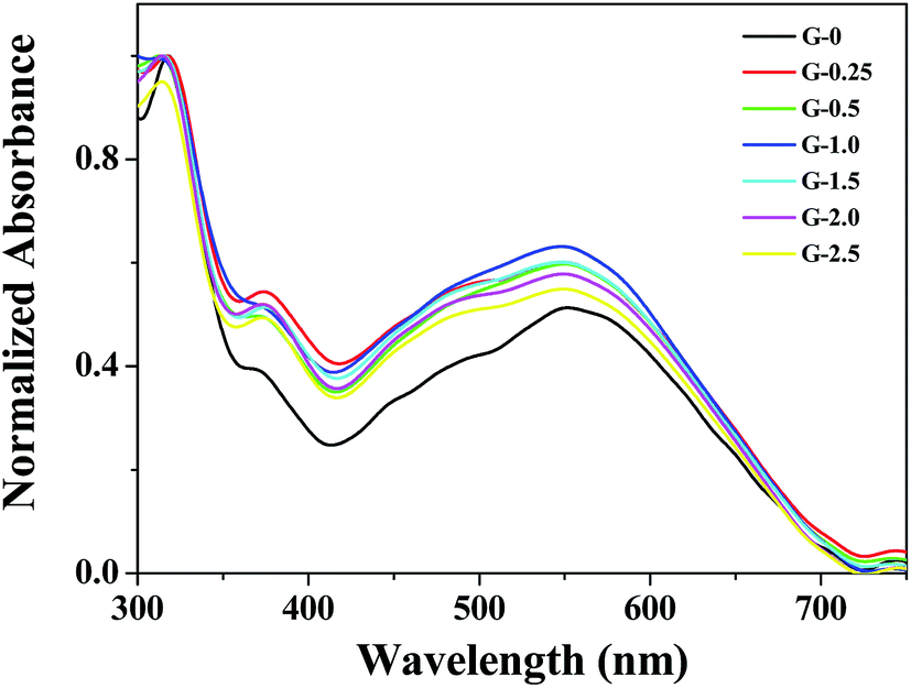 | ||
| Fig. 3 UV-visible absorption spectra of different photoanodes. | ||
| Photoanodes | Dye loading amount/10−7 mol cm−2 |
|---|---|
| G-0 | 1.20 |
| G-0.25 | 1.78 |
| G-0.5 | 1.85 |
| G-1.0 | 1.93 |
| G-1.5 | 1.81 |
| G-2.0 | 1.72 |
| G-2.5 | 1.65 |
To further investigate the influence of rGO on the properties of TiO2 films, the surface photovoltages of different photoelectrodes were investigated, which is a well-established contactless technique for surface state distribution. The curves in Fig. 4 indicate that rGO/TiO2 photoanode could result in stronger surface photovoltage signals between 300 and 750 nm. The surface photovoltage signals increased in the order of G-1.0 > G-1.5 > G-0.5 > G-0.25 > G-2.0 > G-2.5 > G-0, which indicates that the separation efficiency of electrons and holes correlate strongly with rGO amount, the enhancement of the surface photovoltage signals in the region of 300–750 nm is attributed to the increased dye loading amount and the electronic pathway provided by rGO, which helps in effective separation of photogenerated electrons from CB of TiO2 films.
 | ||
| Fig. 4 SPS of different rGO/TiO2 photoanode. | ||
3.2. Performance of DSSCs based on rGO/TiO2 photoanodes
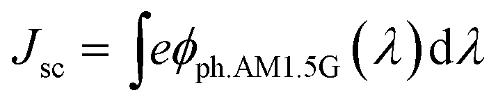
The photovoltaic performance of DSSCs were investigated under a simulated solar irradiation of 100 mW cm−2 (AM1.5G). The photocurrent density–photovoltage (J–V) characteristic of the DSSCs devices based on different photoanodes are shown in Fig. 5 and are used to examine critical photovoltaic parameters such as the open-circuit voltage (Voc), and short-circuit photocurrent density (Jsc). The fill factor (FF) and power conversion efficiency (η) of DSSCs can be also obtained accordingly as interpreted in experimental section. All of these photovoltaic parameters are summarized in Table 2. The device without rGO (G-0) was found to exhibit η value of 5.97% (with Jsc = 13.56 mA cm−2, Voc = 0.70 V, and FF = 0.63), the G-0.25, G-0.5, G-1.0, G-1.5, G-2.0 and G-2.5 devices exhibited η value of 6.03% (with Jsc = 14.02 mA cm−2, Voc = 0.71 V, and FF = 0.61), 6.33% (with Jsc = 14.89 mA cm−2, Voc = 0.71 V, and FF = 0.60), 6.69% (with Jsc = 15.23 mA cm−2, Voc = 0.71 V, and FF = 0.62), 6.37% (with Jsc = 15.10 mA cm−2, Voc = 0.71 V, and FF = 0.60), 5.73% (with Jsc = 14.41 mA cm−2, Voc = 0.69 V, and FF = 0.58) and 4.90% (with Jsc = 12.88 mA cm−2, Voc = 0.66 V, and FF = 0.57), respectively. It is obvious that the use of rGO in TiO2 films significantly improved the power conversion efficiency of the devices. This is because rGO could enhance the dye loading amount and improved light utilization efficiency of photoanode. Meanwhile, rGO was an excellent conductive material, which could improve the electron transport in photoanode and could act as an electron transfer channel.41 Furthermore, rGO restrained recombination and backreaction, which favored the decrease of a diffusive hindrance in electron transfer and improvement of photovoltaic efficiency. Meanwhile, with the addition of rGO (from G-0 to G-1.0), the Jsc and the η were promoted gradually. However, with the further addition of rGO (from G-1.5 to G-2.5), the excess rGO act as a kind of recombination center instead of providing an electron pathway that resulted in longer charge migration routes or electron contacting directly with FTO to form a dark current due to more rGO surrounding TiO2 nanoparticles. Therefore, the moderate addition of rGO was beneficial to the improvement of photovoltaic properties. | ||
| Fig. 5 J–V curves of the DSSCs based on different photoanodes. | ||
| Photoanodes | Jsc (mA cm−2) | Voc (V) | FF | η (%) |
|---|---|---|---|---|
| G-0 | 13.56 | 0.70 | 0.63 | 5.97 |
| G-0.25 | 14.02 | 0.71 | 0.61 | 6.03 |
| G-0.5 | 14.89 | 0.71 | 0.60 | 6.33 |
| G-1.0 | 15.23 | 0.71 | 0.62 | 6.69 |
| G-1.5 | 15.10 | 0.71 | 0.60 | 6.37 |
| G-2.0 | 14.41 | 0.69 | 0.58 | 5.73 |
| G-2.5 | 12.88 | 0.66 | 0.57 | 4.90 |
The enhanced performance of DSSCs based on rGO modified TiO2 semiconductor material was mainly attributed to the enhanced electron transport and restrained charge recombination or back reaction of photoanode by rGO. As show in Fig. 6, the photogenerated electrons in the CB of TiO2 (−4.2 eV) were accelerated into the external circuit via moderate addition of rGO, as the energy level of rGO (−4.4 eV) is between the TiO2 and FTO (−4.7 eV). The TiO2 received the photogenerated electrons from the photoactivated dye. Then, the photogenerated electrons were captured and were transported to FTO without resistance, which limited the charge recombination and back reaction. However, the excessive addition of GO will generate more charge trap on the surface of rGO/TiO2 film to decrease Jsc.
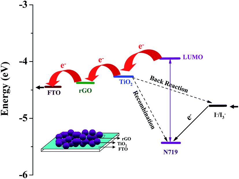 | ||
| Fig. 6 Schematic diagram of electron transport in DSSCs base on rGO/TiO2 photoanodes. | ||
Besides rGO, graphene (Gr) and GO was also widely used to improve the charge transfer in DSSCs. Therefore, the obtained efficiency of the present study is also compared with the previous studies and is summarized in Table 3. These previous reports suggest that the DSSC performance of TiO2 can be improved with the addition of Gr, GO, or rGO. Based on the different graphene fabrication methods, such as electrospinning,42 high temperature reduction,18,43 or different functions of graphene, such as formation of rGO–TiO2 Schottky junction44 or formation of graphene/multi-walled carbon nanotube/TiO2 hybrid,18 the DSSC efficiency also varied. In our present work, rGO/TiO2 was prepared by reducing GO with L-ascorbic acid under mild conditions and used in photoanode. Moreover, the devices in our present work are made without scattering layers, TiCl4 treatment, or antireflecting coatings, but it showed the conversion efficiency of 6.69%, which is much higher or comparable to that of the previously reported DSSCs based on rGO/TiO2, Gr/TiO2, or GO/TiO2.
| Photoanodes | Fabrication method or function | Jsc (mA cm−2) | Voc (V) | FF | η (%) | [Ref.] |
|---|---|---|---|---|---|---|
| Gr/TiO2 | Electrospinning | 12.78 | 0.82 | 0.62 | 6.49 | 42 |
| Gr/TiO2 | Merchandise | 19.92 | 0.70 | 0.49 | 6.86 | 45 |
| Gr/TiO2 | Ball milling | 10.28 | 0.62 | 0.64 | 5.09 | 46 |
| Gr/MWCNTs/TiO2 | High temperature reduction | 11.27 | 0.78 | 0.70 | 6.11 | 18 |
| GO/TiO2 | Hummers method, GO used as template | 9.60 | 0.66 | 0.73 | 4.65 | 47 |
| rGO/TiO2 | Formation of rGO/TiO2 Schottky junction | 18.20 | 0.58 | 0.58 | 6.06 | 45 |
| rGO/TiO2 | High temperature reduction, with TiO2 compact layer | 14.41 | 0.69 | 0.58 | 5.73 | 44 |
| rGO/TiO2 | L-Ascorbic acid reduction | 15.23 | 0.71 | 0.62 | 6.69 | This work |
Particularly, the enhanced Jsc value in our rGO/TiO2 based DSSCs is ascribed to the enhanced IPCE response of the cell, since they are related by the equation:
 | ||
| Fig. 7 IPCE spectra of the DSSCs based on different photoanodes. | ||
3.3. Electrochemical impedance spectroscopy (EIS) analysis of DSSCs
In an effort to get more information about the electron transport in different devices, their electrochemical impedance spectra (EIS) were measured under standard AM1.5G solar irradiation by applying a forward bias of −0.75 V. Under light illumination, EIS was utilized to analyze the electron transport resistance at the TiO2/dye/electrolyte interface for its significance on the efficiency of DSSCs.49 As shown in Fig. 8a, the intersection of the high-frequency semicircle at the real axis represents the equivalent series resistance of the device (Rs), the three semicircles located in high, middle and low frequency regions (left to right) are attributed to the electrochemical reaction at the Pt/electrolyte interface, the electron transfer at the TiO2/dye/electrolyte interface and charge transfer in the electrolyte (Nernst diffusion).50 Since the Rs value remains fairly constant and the DSSC components are the same except for the different concentrations of rGO in the photoanode, the Rs value can be ignored. Meanwhile, the radius of the large semicircle located in middle frequency regions in the Nyquist plots decrease after less amount of rGO than that in G-2.0 was introduced into photoanode, and the values are in the order of G-1.0 < G-1.5 < G-0.5 < G-0.25 < G-0 < G-2.0 < G-2.5, which indicates a decrease of the electron transfer impedance (Rct) and a increase of electron transfer rate at this interface after appropriate amount rGO was introduced, resulting in increase of Jsc value. Based on the Bode plot (Fig. 8b), the frequency was shifted to the higher frequency region with the addition of less amount of rGO than that in G-2.0. Since fmax is inversely associated with the electron transport time in illumination condition τs = 1/(2πfmax),52,53 the increase in fmax indicated a increased rate of the charge-transport process in the DSSC. Hence, electron with shorter τs value indicates that electrons are collected at the FTO electrode at a faster rate. | ||
| Fig. 8 (a) Nyquist plots (b) Bode plots of DSSCs based on different photoanodes measured under standard AM1.5G solar irradiation, and (c) Nyquist plots (d) Bode plots of DSSCs based on different photoanodes measured in dark. | ||
Meanwhile, in an effort to investigate the kinetics of recombination processes, electrochemical impedance spectra (EIS) of devices based on different photoelectrodes were measured in dark by applying a forward bias of −0.75 V. In the dark, the DSSCs behave as a leaking capacitor. Upon forward bias, the electrons are injected from the FTO substrate into the TiO2 and the film is charged by electron propagation through the mesoscopic TiO2 network. Meanwhile, a fraction of the injected conduction band electrons are lost by the reduction of I3− ions present in the electrolyte. Therefore, we could measure impedance spectra of DSSCs in the dark to study the charge recombination from the conduction band of TiO2 to I3− ions. In dark conditions, as shown in Fig. 8c, similar to the condition under illumination, the three semicircles located in high, middle and low frequency regions (left to right) of Nyquist plots are attributed to the redox reaction at the Pt counter electrode, the electron transfer at the TiO2/dye/electrolyte interface and charge transfer in the electrolyte (Nernst diffusion).43 Therefore the larger semicircle observed in middle frequency region represents the resistances of the charge transfer from the TiO2 to the electrolyte (back recombination resistance Rrec). The radius of this semicircle increased after less amount of rGO than that in G-2.0 was introduced, indicating an increase of Rrec. A large Rrec means the small charge recombination rate and vice versa. The radius of the semicircle observed in middle frequency range lies in the order of G-1.0 > G-1.5 > G-0.5 > G-0.25 > G-0 > G-2.0 > G-2.5, indicating sequence of Rrec at the TiO2/dye/electrolyte interface. The increased value of Rrec for DSSCs implies the retardation of the charge recombination between injected electron and I3− ions in the electrolyte. Based on the Bode plot (Fig. 8d), the frequency was shifted to the lower frequency region with the addition of less amount of rGO than that in G-2.0. Since fmax is inversely associated with the electron lifetime in dark condition τn = 1/(2πfmax),51,52 the decrease in fmax indicated a reduced rate of the charge-recombination process in the DSSC. Hence, electrons with longer τn values were prevented from recombining, characterized by a larger Rrec.
Furthermore, Table 4 summarizes the results obtained from the Nyquist plots. The rGO/TiO2 photoanode exhibited a faster electron transport time (τs = Rct × Cu)51,52 than TiO2. Hence, its electron lifetime (τn = Rrec × Cu)51,52 was significantly increased, and recombination was prevented. The photovoltaic performance of the DSSC was clearly reflected by the charge collection efficiency (ηc) derived from ηc = (1 + Rct/Rrec)−1.52,53 Eventually, the charge collection efficiency was significantly increased upon the addition of proper amount of rGO. Therefore, we can conclude that as a result of the longer τn and larger Rrec, the devices fabricated using the optimum rGO/TiO2 photoanode showed improved Jsc values compared to the TiO2 photoanode-based DSSC.
| Photoanode | Rct (Ω) | Rrec (Ω) | Cu (μF) | τs (ms) | τn (ms) | ηc (%) |
|---|---|---|---|---|---|---|
| a The electrochemical impedance spectra (EIS) were recorded at an applied bias of −0.75 V in the frequency range of 0.01 Hz to 100 kHz. Rct: charge transfer resistance; Rrec: charge recombination resistance; Cu: chemical capacitance; τs: electron transport time; τn: electron lifetime; ηc: charge collection efficiency. | ||||||
| G-0 | 14.88 | 24.93 | 6.37 | 0.095 | 0.16 | 63 |
| G-0.25 | 12.44 | 26.62 | 7.44 | 0.093 | 0.20 | 68 |
| G-0.5 | 9.18 | 30.13 | 9.65 | 0.089 | 0.29 | 77 |
| G-1.0 | 7.46 | 36.45 | 11.36 | 0.085 | 0.41 | 83 |
| G-1.5 | 8.15 | 34.22 | 10.51 | 0.086 | 0.36 | 81 |
| G-2.0 | 15.92 | 20.08 | 5.98 | 0.095 | 0.12 | 56 |
| G-2.5 | 18.38 | 18.42 | 5.26 | 0.097 | 0.10 | 50 |
The EIS analysis of different DSSCs in Fig. 8 also confirms that excess amount of rGO in TiO2 photoanode act as a kind of recombination center instead of providing an electron pathway that resulted in longer charge migration routes or electron contacting directly with FTO to form a dark current due to more rGO surrounding TiO2 nanoparticles.
3.4. Dark current measurement of DSSCs
The results mentioned above are also supported by dark current–voltage (J–V) measurements of different devices. Dark current measurement in DSSC cannot be related directly to the back electron transfer process, since the electrolyte concentration in the films and the potential distribution across the nanoporous electrode in dark are different than those under illumination.53 However, a comparison of dark current between the investigated cells can provide useful information regarding the back electron transfer process. Therefore, dark current measurement of DSSCs has been considered as a qualitative technique to describe the extent of the back electron transfer.54 Fig. 9 shows the dark current–voltage characteristics of the DSSCs based on different photoelectrodes with the applied bias from 0 to +0.80 V. The onset of the dark current for G-0 device occurs at a bias about +0.30 V, with a subsequent dramatic increase of dark current with the increase of potential. In contrast, for the G-0.25, G-0.5, G-1.0 and G-1.5 devices, the onset potential shifted gradually to about +0.40 V. Furthermore, the dark current of these rGO modified DSSCs increased much slower than that of G-0 device when potential was greater than +0.40 V. In other words, under the same potential bias, when the potential was ≥0.4 V, the dark current for the G-0.25, G-0.5, G-1.0 and G-1.5 modified DSSCs was noticeably smaller than that for the G-0 device. The increase of the onset potential and the reduction of the dark current demonstrated that moderate addition of rGO successfully suppress the electron back reaction with I3− in the electrolyte by providing a fast and direct electron transport pathway. This is critical to reduce the current leakage in DSSC and enhance its efficiency. However, excess amount of rGO in TiO2 photoanode act as a kind of recombination center instead of providing an electron pathway that resulted in a larger dark current. | ||
| Fig. 9 Dark current of the DSSCs based on different photoanodes. | ||
3.5. Open circuit voltage decay of DSSCs
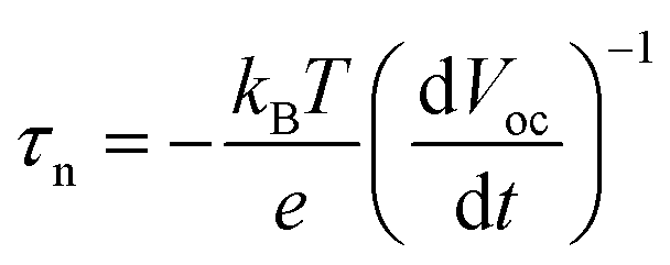
To further probe the recombination kinetics of the devices, open-circuit voltage decay (OCVD) curves were recorded. In order to conduct the OCVD measurement, the simulated solar light is illuminated at DSSCs and a steady-state voltage was obtained. This indicated that equilibrium between electron injection and recombination is attained at the FTO surface. A potentiostat then monitors the decay of Voc after interrupting the illumination. The decay of the photovoltage reflects the decrease of the electron concentration at the FTO surface, which is mainly caused by the charge recombination. In other words, the recombination velocity of photoelectron is proportional to the response of the OCVD.55 Fig. 10a shows the OCVD decay curves of different devices. It was observed that the OCVD response of G-0.25, G-0.5, G-1.0 and G-1.5 were much slower than that of G-0 device, especially in the shorter time domain (within 15 s). The correlation between Voc decay and electron lifetime (τn) can be expressed by equation:where kB is the Boltzmann constant, T is temperature, and e is the electron charge.53 Therefore, the electron lifetimes can be extracted from the initial slope of Voc decay curves. Fig. 10b compares the results of the dependence of τn on the open-circuit voltage for DSSCs with and without rGO modified photoanode. It clearly demonstrates that, at any given open-circuit potential, the electron life of the solar cell with G-0.25, G-0.5, G-1.0 and G-1.5 photoanode was longer than that of G-0 device. This suggests that the electrons injection from excited dye can survive longer and hence can facilitate electron transport without undergoing losses at the bare FTO surface. In conclusion, the OCVD measurement in Fig. 10 demonstrated that introduction of moderate amount rGO into TiO2 photoanode was able to reduce the photoelectron recombination speed effectively and prolong the lifetime of the photoelectrons. However, introduction of excess amount rGO into TiO2 photoanode will obtain opposite results. All of these results match well with the photovoltaic and EIS analyses of different devices.
 | ||
| Fig. 10 (a) The OCVD curves of the DSSCs with different photoanodes; (b) the electron lifetime as a function of Voc of the DSSCs with different photoelectrodes. | ||
4. Conclusions
In conclusion, reduced graphene oxide (rGO) was prepared by reduction of graphene oxide (GO) under mild conditions and was applied to modify TiO2 semiconductor materials for dye-sensitized solar cells. After the moderate amount addition of rGO, the photoanodes displayed enhanced dye adsorption properties with lower internal resistances, faster electron transport and lower charge recombination rate, which resulted in high current density. At the optimum rGO concentration, the DSSC exhibited a Jsc of 15.23 mA cm−2, a Voc of 0.71 V, and a FF of 0.62 with the energy conversion efficiency (η) of 6.69%, indicating a increase in Jsc and η respectively than that of DSSC based on unmodified TiO2 photoanode, which gives a Jsc of 13.56 mA cm−2, a Voc of 0.70 V, and a FF of 0.63 with a η of 5.97%. However, the addition of excess rGO weakened the crystallization of particles on the surface of photoelectrodes and acted as a kind of recombination center, which led to the enhancement of charge recombination, the reduction of dye adsorption and the decrease of photoelectric conversion efficiency of DSSCs.Acknowledgements
This work was supported by National Natural Science Foundation of China (Grant 21571042, 21171044, 21371040, 21203058 and 51307046) and the National key Basic Research Program of China (973 Program, 2013CB632900), the National Key Technology Support Program of China (No. 2013BAE04B03), the Science Foundation for Youths of Heilongjiang Province of China (Grant NO. QC2016013), the Foundation of Educational Commission of Heilongjiang Province of China (No. 12531579) and the Innovative Talents Program of Heilongjiang University of Science and Technology (Q20130202).References
- B. O'Regan and M. Grätzel, Nature, 1991, 353, 737–740 CrossRef.
- M. Grätzel, Acc. Chem. Res., 2009, 42, 1788–1798 CrossRef PubMed.
- L. Kavan, Top. Curr. Chem., 2014, 348, 53–94 CrossRef PubMed.
- L. Kavan, J. H. Yum and M. Grätzel, Electrochim. Acta, 2014, 128, 349–359 CrossRef CAS.
- F. A. Jumeri, H. N. Lim, Z. Zainal, N. M. Huang, A. Pandikumar and S. P. Lim, J. Power Sources, 2015, 293, 712–720 CrossRef CAS.
- S. P. Lim, A. Pandikumar, Y. S. Lim, N. M. Huang and H. N. Lim, Sci. Rep., 2014, 4, 5305 Search PubMed.
- C. K. Dong, W. C. Xiang, F. Z. Huang, D. C. Fu, W. C. Huang, U. Bach, Y. B. Cheng, X. Li and L. Spiccia, Nanoscale, 2014, 6, 3704–3711 RSC.
- T. Chen, S. Wang, Z. Yang, Q. Feng, X. Sun, L. Li, Z. S. Wang and H. Peng, Angew. Chem., Int. Ed., 2011, 50, 1815–1819 CrossRef CAS PubMed.
- M. Grätzel, J. Photochem. Photobiol., C, 2003, 4, 145–153 CrossRef.
- X. Fang, M. Li, K. Guo, X. Liu, Y. Zhu, B. Sebo and X. Zhao, Sol. Energy, 2014, 101, 176–181 CrossRef CAS.
- J. van de Lagemaat, N. G. Park and A. J. Frank, J. Phys. Chem. B, 2000, 104, 2044–2052 CrossRef CAS.
- A. Kongkanand, D. R. Martínez and P. V. Kamat, Nano Lett., 2007, 7, 676–680 CrossRef CAS PubMed.
- A. Kongkanand and P. V. Kamat, ACS Nano, 2007, 1, 13–21 CrossRef CAS PubMed.
- M. Kovendhan, D. P. Joseph, P. Manimuthu, S. Sambasivam, S. N. Karthick, K. Vijayarangamuthu, A. Sendilkumar, K. Asokan, H. J. Kim, B. C. Choi, C. Venkateswaran and R. Mohan, Appl. Surf. Sci., 2013, 284, 624–633 CrossRef CAS.
- Y. D. Duan, J. Zheng, M. Xu, X. Song, N. Fu, Y. Fang, X. Zhou, Y. Lin and F. Pan, J. Mater. Chem. A, 2015, 3, 5692–5700 CAS.
- A. R. Tanyi, A. I. Rafieh, P. Ekaneyaka, A. L. Tan, D. J. Young, Z. Zheng, C. Vijila, G. S. Subramanian and R. L. N. Chandrakanthi, Electrochim. Acta, 2015, 178, 240–248 CrossRef CAS.
- M. Adachi, Y. Murata, J. Takao, J. Liu, M. Sakamoto and F. Wang, J. Am. Chem. Soc., 2004, 126, 14943–14949 CrossRef CAS PubMed.
- M. Y. Yen, M. C. Hsiao, S. H. Liao, P. I. Liu, H. M. Tsai, C. C. M. Ma, N. W. Pu and M. D. Ger, Carbon, 2011, 49, 3597–3606 CrossRef CAS.
- Y. Lai, H. Zhuang, K. Xie, D. Gong, Y. L. Tang, C. L. Sun and Z. Chen, New J. Chem., 2010, 34, 1335–1340 RSC.
- J. M. Macak, F. Schmidt-Stein and P. Schmuki, Electrochem. Commun., 2007, 9, 1783–1787 CrossRef CAS.
- L. Yang, D. He, Q. Cai and C. A. Grimes, J. Phys. Chem. C, 2007, 111, 8214–8217 CAS.
- H. Zhao, Y. Chen, X. Quan and X. Ruan, Chin. Sci. Bull., 2007, 52, 1456–1461 CrossRef CAS.
- N. Yang, J. Zhai, D. Wang, Y. Chen and L. Jiang, ACS Nano, 2010, 4, 887–894 CrossRef CAS PubMed.
- C. H. Ng, H. N. Lim, S. Hayase, I. Harrison, A. Pandikumar and N. M. Huang, J. Power Sources, 2015, 296, 169–185 CrossRef CAS.
- Y. H. Ng, I. V. Lightcap, K. Goodwin, M. Matsumura and P. V. Kamat, J. Phys. Chem. Lett., 2010, 1, 2222 CrossRef CAS.
- R. Nair, P. Blake, A. Grigorenko, K. Novoselov, T. Booth, T. Stauber, N. Peres and A. Gein, Science, 2008, 320, 1308 CrossRef CAS PubMed.
- S. Stankovich, D. A. Dikin, G. H. Dommett, K. M. Kohlhaas, E. J. Zimney, E. A. Stach, R. D. Piner, S. T. Nguyen and R. S. Ruoff, Nature, 2006, 442, 282–286 CrossRef CAS PubMed.
- D. Li and R. B. Kaner, Science, 2008, 320, 1170 CrossRef CAS PubMed.
- Y. Si and E. T. Samulski, Nano Lett., 2008, 8, 1679–1982 CrossRef CAS PubMed.
- G. Williams, B. Seger and P. V. Kamat, ACS Nano, 2008, 2, 1487–1491 CrossRef CAS PubMed.
- X. Fang, M. Li, K. Guo, Y. Zhu, Z. Hu, X. Liu, B. Chen and X. Zhao, Electrochim. Acta, 2012, 65, 174–178 CrossRef CAS.
- B. Tang, G. Hu, H. Gao and Z. Shi, J. Power Sources, 2013, 234, 60–68 CrossRef CAS.
- Z. Xiang, X. Zhou, G. Wan, G. Zhang and D. Cao, ACS Sustainable Chem. Eng., 2014, 2, 1234–1240 CrossRef CAS.
- C. H. Shan, H. Zhan, W. L. Chen, Z. M. Su and E. B. Wang, J. Mater. Chem. A, 2016, 4, 3297–3303 CAS.
- W. Song, C. He, W. Zhang, Y. Gao, Y. Yang, Y. Wu, Z. Chen, X. Li and Y. Dong, Carbon, 2014, 77, 1020–1030 CrossRef CAS.
- J. L. Zhang, H. J. Yang, G. X. Shen, P. Cheng, J. Y. Zhang and S. W. Guo, Chem. Commun., 2010, 46, 1112–1114 RSC.
- P. Y. Reddy, L. Giribabu, C. Lyness, H. J. Snaith, C. Vijaykumar, M. Chandrasekharam, M. Lakshmikantam, J. H. Yum, K. Kalyanasundaram, M. Grätzel and M. K. Nazeeruddin, Angew. Chem., Int. Ed., 2007, 46, 373–376 CrossRef CAS PubMed.
- D. A. Dikin, S. Stankovich, E. J. Zimney, R. D. Piner, G. H. B. Dommett, G. Evmenenko, S. T. Nguyen and R. S. Ruoff, Nature, 2007, 448, 457–460 CrossRef CAS PubMed.
- F. Xu, J. Chen, X. Wu, Y. Zhang, Y. Wang, J. Sun, H. Bi, W. Lei, Y. Ni and L. Sun, J. Phys. Chem. C, 2013, 117, 8619–8627 CAS.
- S. P. Lim, N. M. Huang and H. N. Lim, Ceram. Int., 2013, 39, 6647–6655 CrossRef CAS.
- J. Zhao, J. Wu, F. Yu, X. Zhang, Z. Lan and J. Lin, Electrochim. Acta, 2013, 96, 110–116 CrossRef CAS.
- P. Zhu, A. S. Nair, S. Peng, S. Yang and S. Ramakrishna, ACS Appl. Mater. Interfaces, 2012, 4, 581–585 CAS.
- S. P. Lim, A. Pandikumar, N. M. Huang and H. N. Lim, Int. J. Energy Res., 2015, 39, 812–824 CrossRef CAS.
- J. Song, Z. Yin, Z. Yang, P. Amaladass, S. Wu, J. Ye, Y. Zhao, W. Q. Deng, H. Zhang and X. W. Liu, Chem.–Eur. J., 2011, 17, 10832–10837 CrossRef CAS PubMed.
- T. H. Tsai, S. C. Chiou and S. M. Chen, Int. J. Electrochem. Sci., 2011, 6, 3333–3343 CAS.
- X. Fang, M. Li, K. Guo, Y. Zhu, Z. Hu, X. Liu, B. Chen and X. Zhao, Electrochim. Acta, 2012, 65, 174–178 CrossRef CAS.
- P. Wang, F. He, J. Wang, H. Yu and L. Zhao, Appl. Surf. Sci., 2015, 358, 175–180 CrossRef CAS.
- A. Hagfeldt, G. Boschloo, L. Sun, L. Kloo and H. Pettersson, Chem. Rev., 2010, 110, 6595–6663 CrossRef CAS PubMed.
- C. Y. Hsu, W. T. Chen, Y. C. Chen, H. Y. Wei, Y. S. Yen, K. C. Huang, K. C. Ho, C. W. Chu and J. T. Lin, Electrochim. Acta, 2012, 66, 210–215 CrossRef CAS.
- D. Kuang, S. Uchida, R. Humphry-Baker, S. M. Zakeeruddin and M. Grätzel, Angew. Chem., Int. Ed., 2008, 47, 1923–1926 CrossRef CAS PubMed.
- S. P. Lim, A. Pandikumar, N. M. Huang, H. N. Lim, G. Gu and T. L. Ma, RSC Adv., 2014, 4, 48236–48244 RSC.
- S. P. Lim, A. Pandikumar, N. M. Huang and H. N. Lim, RSC Adv., 2015, 5, 44398–44407 RSC.
- A. Zaban, A. Meier and B. A. Gregg, J. Phys. Chem. B, 1997, 101, 7985–7990 CrossRef CAS.
- S. Ito, P. Liska, P. Comte, R. Charvet, P. Pechy, U. Bach, L. Schmidt-Mende, S. M. Zakeeruddin, A. Kay, M. K. Nazeeruddin and M. Graetzel, Chem. Commun., 2005, 25, 4351–4353 RSC.
- A. Zaban, M. Greenshtein and J. Bisquert, ChemPhysChem, 2003, 4, 859–864 CrossRef CAS PubMed.
| This journal is © The Royal Society of Chemistry 2016 |