
Degradation and regeneration of hybrid perovskites†
Charu Seth and
Deepa Khushalani*
Materials Chemistry Research Group, Department of Chemical Sciences, Tata Institute of Fundamental Research, Homi Bhabha Rd, Colaba, Mumbai, India 400005. E-mail: khushalani@tifr.res.in
First published on 20th October 2016
Abstract
A hybrid organic inorganic perovskite, CH3NH3PbI3, has been deposited, using a two-step deposition technique, on three different substrates: bare FTO and two different types of TiO2 electron transport layers. These structures have then been monitored, using XRD, for degradation under exclusively ultraviolet (UV) and visible light. It has been observed that the topography of the underlying substrate is shown to impose a substantial effect on the particle size of the HOIP phase that gets deposited on top. Furthermore, subsequently it has been observed that the particle size, the level of crystallinity and also type of irradiation (UV vs. visible light) all are important parameters that substantially influence the rate and manner of degradation of HOIPs. These are in addition to the oft-cited parameters such as moisture, O2 and temperature. Moreover, depending on the level of degradation, it has been intriguingly observed that the HOIP phase can be regenerated upon a simple treatment involving I2 deposition. This latter aspect has the potential to circumvent the deleterious degradation that is hindering further progress with this highly promising material.
Introduction
Hybrid organic–inorganic perovskites (HOIPs), such as methyl ammonium lead halides, have garnered a huge interest not only due to their exceptional optoelectronic and light-absorbing properties but also because this has been coupled with a versatile and facile synthesis scheme that can be easily adapted.1,2 The solar cells based on these HOIPs have been shown to have an efficiency of ca. 20% which has been reached in an unprecedentedly short period of time of ca. 6 years.3 As such, HOIPs have been coupled with both organic and sensitized solar cells, with a multitude of electron and hole transporters and in some cases, even with an insulator (Al2O3).4 Despite the several positive attributes of this promising material, a major concern has been the lack of both temporal and thermal stability. The devices are prone to hysteresis in the I–V data within the first cycle and as such the degradation is atypically fast for a conventional perovskite structured material. Many theories abound for the source of this instability and over the last two years there has been an almost exponential rise in the evaluation of the HOIPs in terms of determining the causes of their instability. Table S1† lists most of the major publications that have detailed studies on this instability and it also lists the main conclusions that have been arrived at. Evaluating the aforementioned work in unison, it can be compiled that the most oft-cited reason for degradation appears to be the presence of moisture. It has been shown to affect the chemical and therefore the electronic integrity of the HOIP. This latter aspect can be perturbed by altering the nature of chemical bonds that are present in the lattice. It appears that water inserts into the lattice and disrupts the hydrogen bonding present.5 This leads to complete disruption of the perovskite structure and PbI2 has been shown to form as a by-product.6 Other parameters that have shown to affect degradation are O2 and light. The former aspect appears to have a disruptive effect because of the formation of O2˙− species while irradiation with light appears to have several consequences on the structure. Most of the hypotheses rely on the fact that since HOIPs are ferroelectrics, upon irradiation, dipoles and most likely polarons are formed which lead to alterations in the unit cell dimensions and loss of structural integrity.7 In terms of evaluation of the chemical products formed during degradation, in addition to the hydrated (CH3NH3PbI3·H2O or CH3NH3PbI3·2H2O) form, thus far only PbI2 has been effectively observed through XRD analysis. As such, chemically the reactions mentioned in Scheme 1 are hypothesized to be occurring.8 | ||
| Scheme 1 Proposed mechanism of degradation of perovskite in the presence of moisture and oxygen. | ||
Irrespective of the mechanism of degradation, it is important to note, that for a fully viable solar cell device, all the aforementioned parameters (H2O, O2, light) are present under ambient conditions, and it would be difficult to mitigate their influence during operation of any device. This is especially important if the cost of the device has to be maintained at a reasonable level.
As such, presented here is a study of the XRD evaluation of the formation and degradation of HOIPs, specifically methyl ammonium lead iodide, all the while being exposed to ambient conditions (hence humidity, oxygen and light). We have evaluated two specific parameters: (a) primarily we have explicitly varied the nature of the underlying electron transport layer. Specifically, we have deposited HOIP on a conducting electrode and then subsequently on two different types of TiO2. One consists of the oft-cited P25 phase (nanoparticles of titanium oxide) and the other consists of in situ synthesized TiO2 nanowires, grown uni-directionally on FTO. To the best of our knowledge, this is the first study whereby degradation has been monitored by manipulating the underlying substrate morphology whilst keeping all other parameters constant, even the chemical composition of the underlying electron transport layer. We have observed that surprisingly the morphology and surface roughness of the underlying substrate imparts another condition on the degradation rate of perovskites and therefore it adds to the list of parameters that need to be paid attention to in order to minimize the degradation process. (b) Moreover, we have also evaluated the influence, individually, of UV and visible light on the degradation of these HOIP coated substrates. UV irradiation imposes a more dramatic effect on the degradation rate and this is irrespective of the underlying substrate present.
Furthermore, making a successful, degradation resistant device is possible, but involves deposition of additional layers (e.g., hydrophobic layers to minimize interaction of perovskite with moisture), adding to the cost of the overall device. The current study, in addition to describing the substrate dependent degradation, introduces a simple and cheap method to reverse the degradation itself caused by moisture and light. This method involves treatment of degraded perovskite samples with iodine that, depending on the degree of degradation, regenerates the tetragonal lattice of methyl ammonium lead triiodide as confirmed by the XRD and UV-visible absorption.
Experimental
Analytical grade reagents lead iodide (PbI2), 99% pure (used after recrystallization), hydroiodic acid (HI) (57 wt% aqueous solution, 99.99% pure), titanium butoxide, titanium isopropoxide, titanium dioxide (P25) were purchased from Aldrich. Methylamine solution (CH3NH3I), 33 wt% in absolute ethanol, was purchased from SDF Chemicals, India.Preparation of TiO2 blocking layer on FTO
1 mL of titanium isopropoxide and 0.1 mL acetic acid were mixed with 5 mL ethanol and sonicated for 10 minutes. This solution was spin coated on clean FTO substrates (in two steps – first accelerated to 1000 rpm in 10 seconds and spun for 20 seconds, then accelerated to 2500 rpm in 15 seconds and spun for 60 seconds), following which the substrates were annealed at 450 °C.Preparation of P25 and TiO2 NW films on FTO
A paste of commercial P25 was prepared using a procedure reported by Ito et al.9 This paste was doctor-bladed on TiO2 blocking layer coated FTO. TiO2 nanowires were solvothermally grown on TiO2 blocking layer coated FTO. The procedure was adapted using a procedure reported by Mishra et al.10 A TiO2 blocking layer coated FTO substrate was kept horizontally in a 45 mL Teflon liner to which 250 mg of titanium butanediolate (a precursor for TiO2 synthesis prepared using titanium butoxide using a protocol mentioned in ref. 10) 20 mL hexane and 2 mL of 37% HCl were added. The liner was steel jacketed and was kept in a preheated oven at 135 °C for 3.5 hours. The substrate was subsequently washed with ethanol and deionised water and used for perovskite deposition.Sequential deposition of CH3NH3PbI3 films
10 μL of PbI2 (recrystallized) solution was drop-cast on substrates (FTO, NP/FTO or NW/FTO), following which the substrates were annealed at 90 °C for an hour. The PbI2 coated substrates were dipped in a solution of CH3NH3I in isopropanol (250 mg/12.5 mL) for 20 minutes at 45 °C, following which they were annealed at 90 °C for 1.5 hours.Photo-degradation of CH3NH3PbI3 on various substrates
Three samples – CH3NH3PbI3/FTO, CH3NH3PbI3/NP/FTO, and CH3NH3PbI3/NW/FTO were kept at a distance of 20 cm from a 100 W tungsten lamp or 100 W mercury lamp in a black box covered from all the sides. The X-ray diffractograms of these samples were recorded ex situ after irradiation for different intervals of time. The intensity of (110), (310), and (224) lattice planes were monitored as a function of time of irradiation. During the entire experiment, the samples were kept under constant humidity and temperature. Control experiments were done under dark conditions and these were also maintained at the same humidity and temperature conditions.I2 treatment of degraded HOIP films
A solution of solid iodine (25 mg) was prepared in hexane (1 mL). 50 μL of this solution was drop-cast on the degraded HOIP samples (4 day aged) and allowed to dry in air for a few minutes. The dried samples were subsequently annealed in oven at 90 °C for 2 hours.Characterization
Powder X-ray diffraction (XRD) measurements from 7° to 55° 2θ were recorded using a PANalytical X'pertpro diffractometer with monochromatic CuKα radiation (λ = 1.54056 Å) operating at 40 kV and 30 mA. The surface morphologies of the samples were investigated by Field Emission Scanning Electron Microscopy (FE-SEM) on a Zeiss Ultra FEG 55 instrument at 5 kV operating voltage. The UV-visible absorbance spectra were recorded in diffuse reflectance mode in V-670 Jasco Spectrophotometer at a scan rate of 200 nm min−1. The surface line profiles of the samples were recorded by Ambios Technology XP-2 surface profiler that has a step height resolution of 100 Å.Results
Part I: degradation of HOIP
Initially, three substrates were characterized: bare FTO, P25 (TiO2 nanoparticles) deposited on FTO, and TiO2 nanowires grown in situ on FTO (see Method section for further details). For brevity, these three substrates are referred to as FTO, NP–FTO and NW–FTO respectively. Fig. 1 displays the SEM images of these three substrates and the surface topography can be seen to be relatively smooth for FTO and NP–FTO. However for NW–FTO, the cross sectional image (Fig. 1d) displays the vertically aligned TiO2 rods with apical tips. As such, the three substrates have varying degrees of roughness and their respective surface profile line scans are shown in Fig. S1a.† The average values of film roughness are tabulated in Fig. S1c.† FTO is the smoothest substrate, followed by NP–FTO, and NW–FTO. The line scan of NW–FTO shows large dips owing to the spaces between the aligned nanowires. Upon these three substrates, HOIP was subsequently deposited using an identical method involving sequential deposition (for details, see Method section).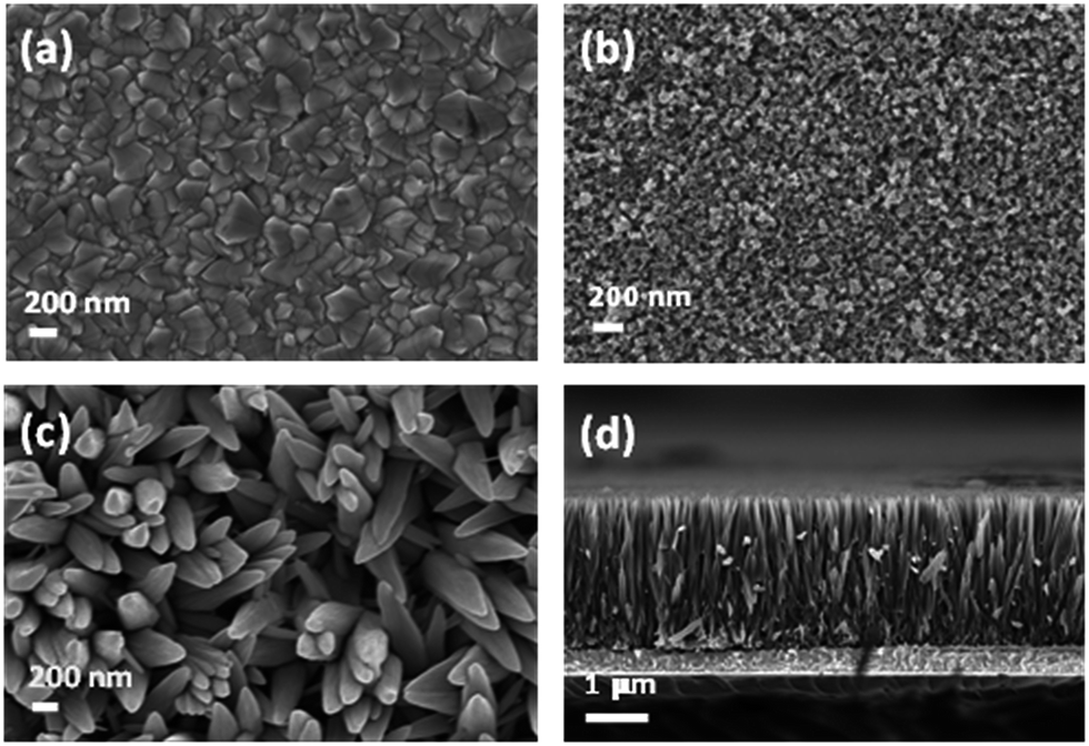 | ||
| Fig. 1 Top view scanning electron micrographs of (a) FTO, (b) NP–FTO, (c) NW–FTO, and (d) cross-sectional view of NW–FTO. | ||
Fig. 2 shows the SEM images of the perovskite layer that was deposited. Interestingly, it can be seen that the HOIP morphology is similar on the FTO and NW–FTO substrates (Fig. 2a and c) however different for NP–FTO (Fig. 2b). For FTO and NW–FTO, a range of sizes are observed, the smallest being irregular spheres about 100 nm in size, rods about 400 nm long, and cuboids about 500 nm in size. However, for NP–FTO, predominantly small particles with sizes less than 200 nm are observed. For clarity, a low magnification image of NW–FTO is also shown in Fig. 2d where a crack in the perovskite layer is imaged to showcase that the underlying TiO2 nanowires have maintained their integrity. For all the three samples, X-ray diffraction analysis confirmed the sole presence of the tetragonal phase of methyl ammonium lead triiodide, Fig. 3.
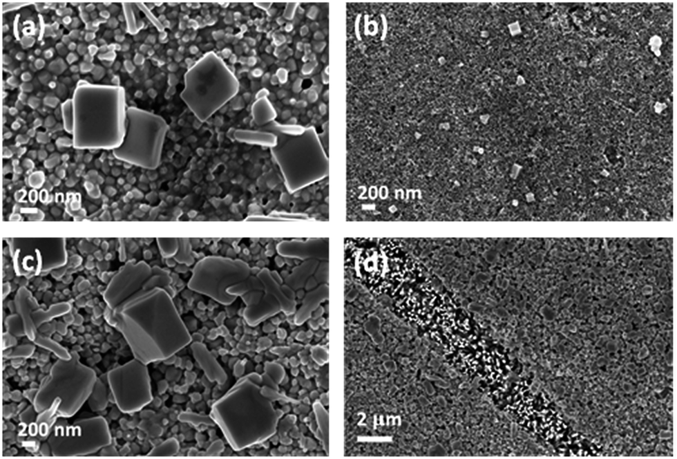 | ||
| Fig. 2 Top view scanning electron micrographs of HOIP coated on (a) FTO, (b) NP–FTO, (c) NW–FTO, and (d) low magnification view of HOIP/NW–FTO showing a crack in the film where NW is visible. | ||
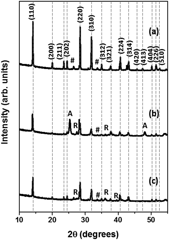 | ||
| Fig. 3 X-ray diffractograms of HOIP coated on (a) FTO, (b) NP–FTO, and (c) NW–FTO. #, A, and R represent FTO, anatase, and rutile peaks, respectively coming from the substrates. | ||
It should be highlighted that the NP–FTO underlying substrate gave additional peaks belonging to rutile and anatase phase while NW–FTO only showed the rutile peaks. The level of crystallinity could be gauged by the full width half maxima (FWHM) of the lattice planes in the XRD patterns.
Table S2† shows the FWHM of the initial crystalline HOIP phase, and it was observed that FWHM of the HOIP on FTO and NW–FTO were similar and consistent while, the HOIP phase on NP–FTO appeared to show disorder and there was anomalous broadening of some lattice planes. This aspect is important as it denotes that the level of crystallinity was similar for HOIP phase grown on FTO and NW–FTO. However there was heterogeneity in the HOIP phase grown on NP–FTO. These films, as deposited were then allowed to age temporally under identical conditions (room temperature at 25 °C, humidity at 65%). Fig. S2† depicts an optical image of the degraded material as observed after 4 days. Visually, the degraded materials appear to be different for the different substrates present. Interestingly, X-ray diffraction patterns of the degraded HOIP on FTO and NW–FTO appear to be quite similar to each other, whereas the XRD pattern is unique for the degraded HOIP layer on NP–FTO, Fig. 4. The degraded sample on FTO and NW–FTO show low intensity peaks corresponding to the tetragonal phase of HOIP and additional peaks appear corresponding to the hydrated HOIP lattice.11 On the other hand, the degraded HOIP on NP–FTO shows prevalence of lead iodide phase along with peaks of HOIP that have dramatically decreased intensity. As a further to this, a systematic temporal study of degradation of HOIP was performed. This was monitored using XRD and the degradation conditions involved irradiating with exclusively UV or visible light, at 65% humidity and since irradiation causes a slight increase in temperature, all the samples (including those maintained under dark conditions) were maintained at 45 °C temperature. Fig. 5 shows the variation in the XRD intensity of peaks for three types of samples-HOIP/FTO, HOIP/NP–FTO, and HOIP/NW–FTO-in dark, and while being irradiated with exclusively UV light and visible light whilst keeping other parameters constant. Peak intensities of (110), (310), and (224) planes were carefully monitored as a function of time. For brevity, the data for only (224) plane has been shown and the trend observed is similar to those obtained for (110) and (310). The decrease in intensity of XRD lattice planes is a signature of loss of crystallinity and therefore loss of structure. As such, the in-dark profiles for all the samples show negligible slopes (Fig. 5a) which implies that little or no decrease in crystallinity and/or degradation is occurring. The profile for UV irradiated samples (Fig. 5b) shows different extents of degradation for the three samples as suggested by the negative slopes. The fastest to degrade was HOIP on NP–FTO, while the rate of decrease in the intensity of the (224) plane for HOIP on FTO and NW–FTO appears to be relatively similar.
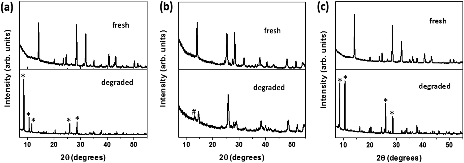 | ||
| Fig. 4 X-ray diffractograms of fresh and degraded HOIP deposited on (a) FTO, (b) NP–FTO, (c) NW–FTO. * Corresponds to major peaks from mono and dihydrated perovskite phase, and # corresponds to PbI2 phase. | ||
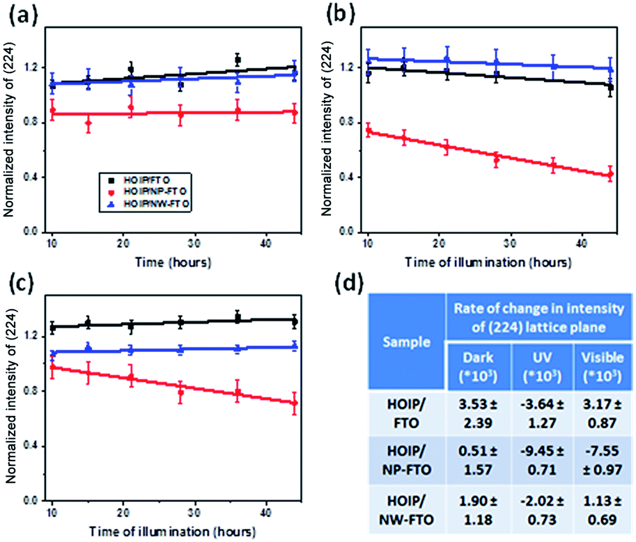 | ||
| Fig. 5 Degradation profiles of HOIP coated on FTO, NP–FTO, and NW–FTO under (a) dark conditions, (b) UV light, and (c) visible light, (d) table showing the values of slopes for the degradation profiles shown in (a), (b), and (c). | ||
The profile for visible light irradiated samples (Fig. 5c) suggests that HOIP on NP–FTO is the most unstable, an observation that correlates with Fig. 5b. The HOIP on FTO and NW–FTO remain stable (under visible light) for 44 hours of experiment as shown by the almost negligible slope of their respective (224) plane intensity. At this point, it needs to be noted that data was plotted only after an elapse of 10 hours since there was in fact an increase in the intensity of the XRD data for FTO and NW–FTO samples during these initial hours of irradiation, Fig. S3.† For these samples, be in-dark or in-light conditions, slightly positive slopes were observed in these first few hours (<10 hours) suggesting some level of re-organization such that crystallinity was being augmented (Fig. S3†). It is being hypothesized that as a temperature of 45 °C was being maintained for all the samples, this was perhaps leading to annealing of the HOIP phase in the initial hours. It was observed that this effect of temperature seemed to be pronounced only in the initial period and other parameters took precedence during the subsequent 10–44 hours that induced degradation.
Part II: regeneration of perovskite
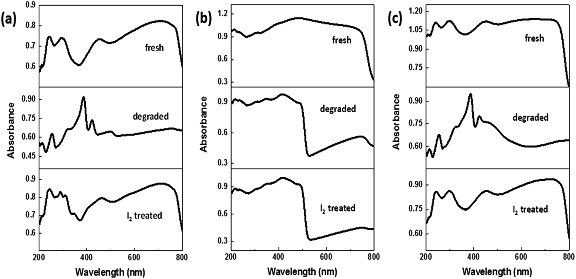
In an attempt to reverse the degradation process observed under ambient conditions (room temperature at 25 °C, humidity at 65%), the aforementioned degraded samples were treated with a solution of iodine in hexane (for details, see Methods section). It was interestingly observed that as soon as the solvent evaporated, the films of the hydrated perovskite phase on FTO and NW–FTO turned black. On the other hand, the yellow film composed of PbI2 on NP–FTO did not show any color change. The resulting three samples were subsequently annealed at 90 °C, following which they were characterized by XRD, DRS, and SEM. The X-ray diffractograms and DRS spectra (Fig. 6 and 7 respectively) show that the I2 treatment appeared to replenish the tetragonal phase HOIP on FTO and NW–FTO. However, on NP–FTO, the PbI2 peak at ca. 12.7° becomes sharper indicating enhancement in crystallinity of the lead iodide, whereas the residual perovskite phase of the partially degraded sample was further suppressed as shown by the reduced intensity of the (110) plane at ca. 14.2°.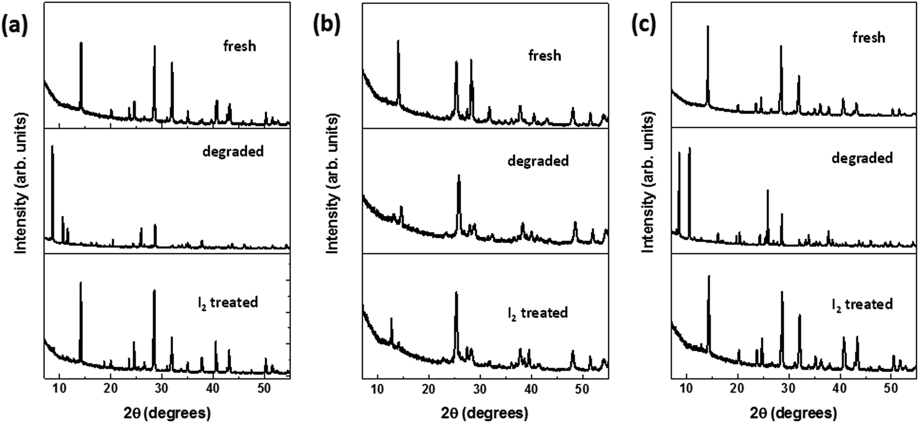 | ||
| Fig. 6 X-ray diffractograms of fresh, degraded, and I2 treated HOIP deposited on (a) FTO, (b) NP–FTO, and (c) NW–FTO. | ||
 | ||
| Fig. 7 Diffuse reflectance spectra of fresh, degraded and I2 treated HOIP deposited on (a) FTO, (b) NP–FTO, and (c) NW–FTO. | ||
Moreover, the DRS spectrum of the I2 treated sample on NP–FTO remained unchanged while again with the FTO and NW–FTO sample, the absorption profile, after I2 treatment, resembled that of the fresh sample. The scanning electron micrographs revealed a change in topography of the HOIP phase, Fig. 8. It can be observed that the regenerated HOIP phase on FTO and NW–FTO appears to now consist of non-faceted structures and a contiguous film is observed, similar to that seen in Fig. 2d.
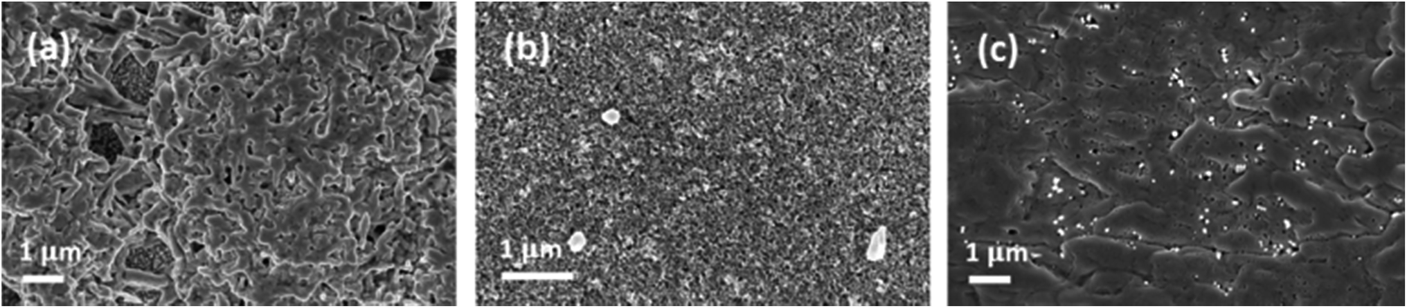 | ||
| Fig. 8 Top view scanning electron micrographs of I2 treated HOIP coated on (a) FTO, (b) NP–FTO, and (c) NW–FTO. | ||
Discussion
Part I: degradation of HOIP
From all the data presented above, it can be surmised that in addition to the oft-cited parameters of humidity, light and temperature that contribute to the degradation of the HOIPs, it appears that the nature of the underlying substrate also plays a pivotal role in the degradation process, or at least contributes to the rate of degradation as well.For these initial 44 hours that were monitored, the HOIP phase formed on FTO and NW–FTO appears to consist of larger particles with better crystallinity when compared to the HOIP phase on NP–FTO. Considering that the same method of deposition was employed, it appears that the physical topography of the underlying substrate and its surface roughness imparts a strain on the depositing HOIP phase such that in some cases smooth nanometer sized particles are obtained which are less ordered and more easily prone to degradation. While for the FTO and NW–FTO substrates, these contributed by aiding a much more organized HOIP phase that seems to be able to withstand degradation to a longer extent. These larger particles are perhaps able to withstand the perturbations on the lattice to a larger extent than the relatively nano-sized crystals that formed on the NP–FTO. This observation corroborates the work showcased by Mohite et al.12 and Song et al.13 who have also stated that level of crystallinity is crucial, and large crystalline grain sizes are better able to contribute to structure (and therefore electronic) stability. Although it is not currently clear as to why the particle sizes are bigger on FTO and NW–FTO, however the observation lends itself to the idea that if robust HOIP layers have to be fabricated, rather than forming nanoparticles of HOIP on any given substrate, it is in fact more important to form structurally ordered HOIP crystalline films and such structures appear to be better at enduring any degradation perturbations.
Furthermore, UV light irradiation seems to have a larger detrimental effect on the HOIP when compared to visible light. The different extents of stability of perovskite on the two different kinds of TiO2 used in this study (TiO2 nanowires and P25) within the time frame of the photo-degradation experiment can be explained by the photoactivity of these two different TiO2. TiO2 is a well-known UV photocatalyst, known to degrade organic materials via the formation of reactive oxygen species. P25 is in fact a model photocatalyst because of the co-existence of two phases: anatase and rutile in a specific ratio of 75![[thin space (1/6-em)]](https://www.rsc.org/images/entities/char_2009.gif) :25 which have a synergistic effect on rate of catalysis.14 As such, it can be inferred that this underlying substrate in fact easily photocatalyzes the degradation of the HOIP phase, while in the case of NW–FTO, the sample, although TiO2 in composition, only consists of the rutile phase10 and hence is not expected to be as efficient a photocatalyst. As such, this sample did not degrade as rapidly in the initial 44 hours. To further prove this aspect, two control experiments were performed whereby the P25 phase was replaced with pure anatase and pure rutile phase. Both these phases now consisted of nanometer sized particles similar to P25. Fig. S4† displays the data for the (224) plane's degradation profile and it can be clearly observed that the better the photocatalyst of the underlying substrate, the more prone to degradation is the HOIP deposited phase. Under UV irradiation, both P25 and pure anatase phases seem to augment the rate of HOIP degradation, whereas the pure rutile phase has less of an impact on the degradation rate. Both P25 and anatase are known to be good photocatalysts as compared to rutile.15,16
:25 which have a synergistic effect on rate of catalysis.14 As such, it can be inferred that this underlying substrate in fact easily photocatalyzes the degradation of the HOIP phase, while in the case of NW–FTO, the sample, although TiO2 in composition, only consists of the rutile phase10 and hence is not expected to be as efficient a photocatalyst. As such, this sample did not degrade as rapidly in the initial 44 hours. To further prove this aspect, two control experiments were performed whereby the P25 phase was replaced with pure anatase and pure rutile phase. Both these phases now consisted of nanometer sized particles similar to P25. Fig. S4† displays the data for the (224) plane's degradation profile and it can be clearly observed that the better the photocatalyst of the underlying substrate, the more prone to degradation is the HOIP deposited phase. Under UV irradiation, both P25 and pure anatase phases seem to augment the rate of HOIP degradation, whereas the pure rutile phase has less of an impact on the degradation rate. Both P25 and anatase are known to be good photocatalysts as compared to rutile.15,16
Part II: regeneration of perovskite
The impetus for I2 treatment emanated from the idea that inorganic perovskites such as CaTiO3, BaTiO3, etc. are commonly known to be oxygen deficient. Moreover a recent theoretical study by Eames et al. alluded to the fact that type and amount of iodide vacancies, that were intrinsically present, were crucial to the electronic properties of HOIP.17 In the fresh HOIP samples reported here, it was observed that in fact I/Pb ratio was lower than the expected value of 3, Table S3.† This aspect is not unique, as Lindblad et al. have previously shown, using photoelectron spectroscopy, that these samples are iodine deficient (and also there is presence of Pb0).18 As such the I2 treatment was performed and intriguingly for two out of the three samples, the HOIP phase appeared to regenerate itself. A regeneration pathway can be proposed by examining the relation between the level of degradation and regeneration of perovskite. This is apparent from the differences between the behavior of FTO (and NW–FTO) and NP–FTO. If the degradation product is PbI2, as on NP–FTO, regeneration of HOIP was found not to be possible and in fact an increase in PbI2 phase was observed; however, if the hydrated phase of HOIP had formed, then an addition of excess I2 appeared to regenerate the HOIP. Therefore, it can be hypothesized that I2 can extract water from the perovskite hydrate and aid the lattice to regenerate when the samples are annealed. This is purported to occur via the following reaction:19| I2 + H2O ⇆ H+ + I− + HIO, E° = −1.45 V |
Furthermore, in the case of HOIP on NP–FTO, it was observed that extraneous PbI2 formed after the I2 treatment. Lindblad et al. had observed that for HOIPs on TiO2 (using also a two-step deposition technique, akin to that detailed above), the stoichiometry was not only deficient in iodine but also metallic lead was detected by photoelectron spectroscopy.18 Therefore, it can be purported that I2 aids in oxidizing any Pb0 that is known to exist and in turn form PbI2. This can be considered viable considering that the standard oxidation potential of Pb0 is 0.13 V and reduction potential of I2 is 0.54 V.20
Conclusions
Presented above is a study involving the degradation and subsequent regeneration of HOIP deposited on three different substrates. It is has been observed that the topography of the substrate is an important parameter that influences the particle size and crystallinity of the HOIP deposited and needs to be controlled even if a well-established deposition technique is being employed. A well-structured HOIP is able to endure for a longer period any degradation perturbations. Moreover, if the underlying support is a photocatalytic oxide, then its behavior, especially under UV light irradiation has a deleterious effect on the degradation pathway. Finally, we have discovered a seminal route to easily regenerating the HOIP phase from its hydrated phases (especially if extraneous PbI2 phase has not formed as yet) by performing a simple I2 treatment.Acknowledgements
The authors would like to acknowledge Ms B Chalke and Mr R Bapat for assistance with electron microscopy, Mr N Kulkarni for help with XRD measurements and training, and Mr A P Shah for help and training to use the surface profiler.References
- J. Im, C. Lee, J. Lee, S. Park and N. Park, Nanoscale, 2011, 3, 4088 RSC.
- T. Baikie, Y. Fang, J. Kadro, M. Schreyer, F. Wei, S. Mhaisalkar, M. Graetzel and T. White, J. Mater. Chem. A, 2013, 1, 5628 CAS.
- N. Park, J. Phys. Chem. Lett., 2013, 4, 2423–2429 CrossRef CAS.
- W. Li, J. Li, L. Wang, G. Niu, R. Gao and Y. Qiu, J. Mater. Chem. A, 2013, 1, 11735 CAS.
- C. Tong, W. Geng, Z. Tang, C. Yam, X. Fan, J. Liu, W. Lau and L. Liu, J. Phys. Chem. Lett., 2015, 6, 3289–3295 CrossRef CAS.
- G. Niu, W. Li, F. Meng, L. Wang, H. Dong and Y. Qiu, J. Mater. Chem. A, 2014, 2, 705–710 CAS.
- W. Nie, J. Blancon, A. Neukirch, K. Appavoo, H. Tsai, M. Chhowalla, M. Alam, M. Sfeir, C. Katan, J. Even, S. Tretiak, J. Crochet, G. Gupta and A. Mohite, Nat. Commun., 2016, 7, 11574 CrossRef CAS PubMed.
- G. Niu, X. Guo and L. Wang, J. Mater. Chem. A, 2015, 3, 8970–8980 CAS.
- S. Ito, P. Chen, P. Comte, M. Nazeeruddin, P. Liska, P. Péchy and M. Grätzel, Prog. Photovoltaics Res. Appl., 2007, 15, 603–612 CrossRef CAS.
- B. Mishra, P. Ghildiyal, S. Agarkar and D. Khushalani, Mater. Res. Express, 2014, 1, 025005 CrossRef.
- M. Shirayama, M. Kato, T. Miyadera, T. Sugita, T. Fujiseki, S. Hara, H. Kadowaki, D. Murata, M. Chikamatsu and H. Fujiwara, J. Appl. Phys., 2016, 119, 115501 CrossRef.
- W. Nie, H. Tsai, R. Asadpour, J. Blancon, A. Neukirch, G. Gupta, J. Crochet, M. Chhowalla, S. Tretiak, M. Alam, H. Wang and A. Mohite, Science, 2015, 347, 522–525 CrossRef CAS PubMed.
- D. Song, J. Ji, Y. Li, G. Li, M. Li, T. Wang, D. Wei, P. Cui, Y. He and J. Mbengue, Appl. Phys. Lett., 2016, 108, 093901 CrossRef.
- M. Henderson, Surf. Sci. Rep., 2011, 66, 185–297 CrossRef CAS.
- T. Luttrell, S. Halpegamage, J. Tao, A. Kramer, E. Sutter and M. Batzilla, Sci. Rep., 2014, 4, 4043 Search PubMed.
- W. Kim, T. Tachikawa, G. Moon, T. Majima and W. Choi, Angew. Chem., Int. Ed., 2014, 126, 14260 CrossRef.
- C. Eames, J. Frost, P. Barnes, B. O'Regan, A. Walsh and M. Islam, Nat. Commun., 2015, 6, 7497 CrossRef CAS PubMed.
- R. Lindblad, D. Bi, B. Park, J. Oscarsson, M. Gorgoi, H. Siegbahn, M. Odelius, E. Johansson and H. Rensmo, J. Phys. Chem. Lett., 2014, 5, 648–653 CrossRef CAS PubMed.
- F. Cotton and G. Wilkinson, Advanced inorganic chemistry, Wiley, New York, 1988 Search PubMed.
- P. Atkins, Physical Chemistry, W. H. Freeman and Company, New York, 6th edn, 2016 Search PubMed.
Footnote |
| † Electronic supplementary information (ESI) available: Surface profile line scans, optical micrographs, XRD profiles in the initial 10 hours of irradiation, FWHM peak data from XRD, and EDX data for I/Pb ratio have been provided. See DOI: 10.1039/c6ra22094k |
| This journal is © The Royal Society of Chemistry 2016 |