DOI:
10.1039/C6RA21955A
(Paper)
RSC Adv., 2016,
6, 103210-103214
An improved model for the surface potential and drain current in negative capacitance field effect transistors
Received
1st September 2016
, Accepted 25th October 2016
First published on 25th October 2016
Abstract
An improved model for the surface potential and drain current in negative capacitance ferroelectric field effect transistors (NC-FeFETs) was presented by introducing the doping concentration. The influence of the doping concentration and temperature on the electric characteristics of NC-FeFET was investigated based on this model. The derived results demonstrated that the subthreshold slope of the metal–ferroelectric–semiconductor NC-FeFET increases, while the drive current decreases when the substrate doping concentration increases from 1017 m−3 to 1020 m−3. Additionally, in the temperature range from 290 K to 380 K, the voltage amplification gradually shrinks, resulting in the subthreshold swing increasing from 51 mV dec−1 to 71 mV dec−1. These results indicated that silicon doping concentration and temperature are two key factors for optimizing the operation voltage in NC-FeFETs.
Introduction
It is well known that the ongoing scaling of field effect transistors urges people to find effective ways to reduce the power dissipation in the process of switching events. A key factor limiting the low voltage operation is the subthreshold swing (SS), which means that the voltage is needed for changing one order of magnitude of drain current. In recent years, the use of ferroelectric negative capacitance (NC) in the gate stack of a metal oxide semiconductor field effect transistor (MOSFET) considered to be an effective way of reducing the SS of complementary metal oxide semiconductor (CMOS) devices below 60 mV dec−1 has been widely investigated from both theoretical and experimental aspects.1–14 For example, Salahuddin and Datta firstly proposed that the physical limitation of SS (60 mV dec−1) can be reduced by replacing the conventional insulator in MOSFETs with a ferroelectric insulator.1 They tried to exploit a negative capacitance regime of the ferroelectric in which the surface potential (φs) of the semiconductor is up-converted and therefore the body factor of the transistor defined by m ≡ ∂Vg/∂φs, where Vg is the gate voltage, becomes smaller than one. Based on this idea, Jiménez et al. proposed a physically-based analytical surface potential and drain current model and optimized the performance of metal–ferroelectric–semiconductor (MFS) FET in terms of gain and Vg range by using properly engineered ferroelectric materials.3 Then, the group of Salahuddin demonstrated that temperature is an effective tuning parameter for the ferroelectric negative capacitance.6 Based on this result, Tang's group proposed a physical model and optimized the SS of Fe-FET in the temperature range from 280 to 360 K.7 Almost at the same time, Salvatore et al. experimentally confirmed that a temperature dependent negative capacitance (NC) effect exists in a ferroelectric field-effect-transistor (Fe-FET).8 They found that the internal voltage amplification is responsible for the SS reduction in the Fe-FET, and this effect disappears when the temperature is increased close to the Curie temperature because of the narrowing of the NC region and because of the saturation of the amplification. Very recently, Shin's group experimentally demonstrated that the steep switching behavior of a MOS device with SS about 18 mV per decade at 300 K by taking advantage of negative capacitance in a MOS gate stack.14 From the previous reports, one can note that a large number of experimental work had been carried out but few corresponding theoretical work were developed timely. However, Salahuddin and Datta's theoretical work do not validate the transistor' transfer characteristics, especially the value of SS < 60 mV dec−1. Jimenez's work and Xiao's work just considered the undoped silicon substrate case and this is often not the actual case for devices. In this paper, we develop the previous model reported in ref. 3 and 7, and introduce the doping concentration effect into it. For the actual device, doping of silicon for MOSFETs often plays an important role in optimizing the electrical properties. In the following study, a model for the MFS-FET considered lightly doped thin silicon substrate will be proposed. The silicon surface potential, the voltage amplification and the transfer characteristics will be investigated in details. It is expected that this investigation can provide some useful guidelines for the design of fast switching and low power dissipation MOSFETs.
Theoretical model
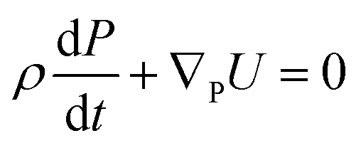
According to the Landau–Khalatnikov (LK) theory, for a nonlinear ferroelectric capacitor, the relationship between the energy (U) and ferroelectric polarization (P) can be expressed as15–17| |
 | (1) |
where| | |
U = αP2 + βP4 + γP6 − Eext·P
| (2) |
is the Gibb's free energy given by the sum of the anisotropy energy and the energy due to the external field Eext, and P is the polarization charge per unit area, α, β, and γ are material dependent constants. It is easily to find that the ferroelectric capacitance (Cf) can be defined as the inverse of the radius curvature of energy (U) versus polarization charge (P) profile of the capacitor, that is to say, Cf = [d2U/dP2]−1.6 For simplicity, the steady-state polarization was considered and dP/dt = 0 was assumed in eqn (1). Combining eqn (1) and (2), one can get the external field.| | |
Eext = 2αP + 4βP3 + 6γP5
| (3) |
Eqn (3) can be further expressed as
| | |
Vf = 2αtfP + 4βtfP3 + 6γtfP5
| (4) |
here,
Vf and
tf represent the voltage drop and thickness of ferroelectric, respectively. The electric displacement or charge per unit area can be expressed as
Q =
P +
ε0E ≈
P, because the value of polarization in a ferroelectric is much bigger than that of
ε0E. Thus the charge–voltage relationship for the gate ferroelectric is
| | |
Vf = 2αtfQ + 4βtfQ3 + 6γtfQ5
| (5) |
This is consistent with the Landau–Ginzburg–Devonshire's (LGD) phenomenological theory,18 in the vicinity of a phase transition, the voltage across the ferroelectric can be expanded in powers of the charge with coefficients that can be experimentally obtained. This is appropriate for a uniaxial ferroelectric as it is being considered in this work. The order of the expansion depends on the type of phase order transition. If the phase transition is of first order (for example, BaTiO3), a fifth-degree odd polynomial is needed, where α, β < 0, and γ > 0.18 If model a second-order phase transition [strontium bismuth tantalite (SBT) could be a typical example], a third-order degree polynomial is needed, where α < 0, β > 0, and γ = 0.18 In the following study, we take SBT as the example of which the exact coefficients are expressed as α = 2.03 × 10⁵(T − 620), β = 3.75 × 10⁹ and γ = 0.18 Neglecting interface traps and space charge, the gate voltage (Vg) applied to the MFS structure as shown in Fig. 1 can be described as
| | |
Vg − Δϕ − φs = 2αtfQ + 4βtfQ3 + 6γtfQ5
| (6) |
where Δ
ϕ is the work function difference between the gate electrode and the semiconductor.
φs is the electrostatic potential in the semiconductor or the surface potential of semiconductor. Unlike the previous work,
3,7 we take Sze's model to describe the relationship of
Q and
φs, and can be written as follows
19| |
 | (7) |
here
LD = (
εs/
qNDβ)
1/2 is the Debye length,
ND stands for the majority carrier concentration and
ni is the intrinsic carrier concentration,
β is defined as
β =
q/
kT with the Boltzmann constant
k, the electronic charge
q and temperature
T. According to Pao and Sah's model, the current from source to drain can be expressed as
20| |
 | (8) |
where
φB = (
kT/
q)ln(
ND/
ni), and
ξ(
φ,
V) is the electric field given by
| |
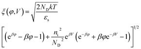 | (9) |
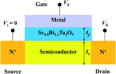 |
| | Fig. 1 Schematic of a MFS-FET structure. | |
According to eqn (6)–(9), the characteristics of Vg–φs, G–Vg, and Vg–Ids can be obtained by numerical methods.
Results and discussion
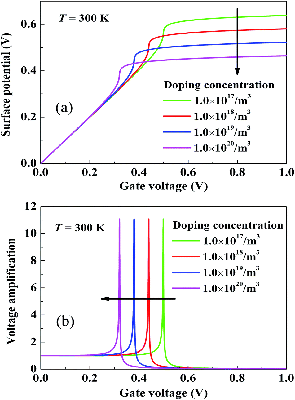
In order to investigate the effect of doping concentration on the silicon surface potential and its amplification, the characteristics of Vg–φs with different doping concentration was shown in Fig. 2(a), and the voltage amplification factor G = ∂φs/∂Vg versus gate voltage was shown in Fig. 2(b). Where, the film thickness of ferroelectric is tf = 35 nm, and the semiconductor is ts = 5 nm. It can be seen from Fig. 2(a) that the magnitude of surface potential gradually decreases with increasing doping concentration from 1.0 × 10¹⁷ m−3 to 1.0 × 10²⁰ m−3. Additionally, the steep increase region of the surface potential shifts left, which results in the voltage amplification point shifts left as shown in Fig. 2(b). However, it should be noted that the doping concentration makes no difference to the voltage amplification factor.
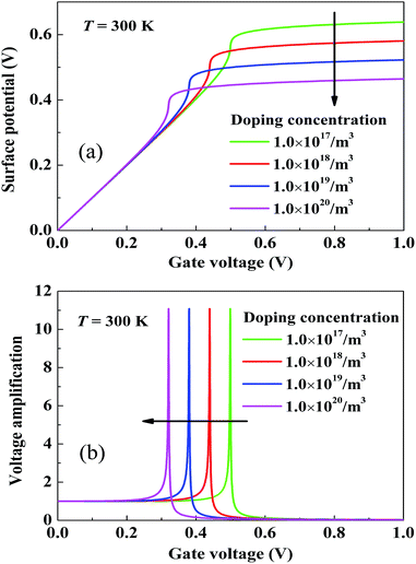 |
| | Fig. 2 Doping concentration effect on (a) the silicon surface potential and (b) the voltage amplification over the gate voltage. | |
Based on this model, the temperature effect on the silicon surface potential and its amplification properties was also investigated in the temperature range from 290 K to 380 K, which is presented in Fig. 3. The doping concentration was kept at 1.0 × 10¹⁷ m−3. From Fig. 3(a), one can clearly see that the amplitude of the surface potential increases with increasing temperature. And the point where the voltage amplification happened shifts right. Interestingly, the steep up-conversion characteristics of the surface potential gradually disappeared when the temperature is high enough, which can also be understood from the voltage amplification factor as shown in Fig. 3(b). For example, the value for the voltage amplification factor is bigger than ten when the temperature is 290 K. However, it rapidly decreases to less than two when temperature is 380 K, which is consistent with the experimental results reported by Salvatore.8
 |
| | Fig. 3 Temperature effect on (a) the silicon surface potential and (b) the voltage amplification over the gate voltage. | |
The transfer property with different doping concentration was demonstrated in Fig. 4. The drain voltage was kept for 0.1 V. It can be obviously seen that the subthreshold slope becomes steeper when improving the doping concentration, indicating that a certain improved doping concentration can improve the subthreshold characteristics of the NC Fe-FET. This is attributed to the shift of peak value of voltage amplification factor towards the lower gate voltage (see Fig. 2(b)). That is to say, the steeper subthreshold slope region corresponds to the region of peak value of voltage amplification and also shifts towards the lower gate voltage. However, in the meanwhile, the drive current decreased remarkably when enhancing the doping concentration, nearly one order of magnitude of the drive current decreased for one order of magnitude of the doping concentration enhanced. This phenomenon can be easily understood from eqn (8). On the one hand, the magnitude of the drive current is dependent on ND−3/2, thus higher doping concentration results in lower drive current. On the other hand, since the doping concentration has no effect on the value of voltage amplification factor G (see Fig. 2(b)), according to the definition of SS = ∂Vg/∂(log10![[thin space (1/6-em)]](https://www.rsc.org/images/entities/char_2009.gif) I) = (∂Vg/∂φs)·(∂φs/∂(log10I)),1 SS is just dependent on the term ∂φs/∂(log10I), so higher doping concentration leads to smaller SS according to Fig. 2(a).
I) = (∂Vg/∂φs)·(∂φs/∂(log10I)),1 SS is just dependent on the term ∂φs/∂(log10I), so higher doping concentration leads to smaller SS according to Fig. 2(a).
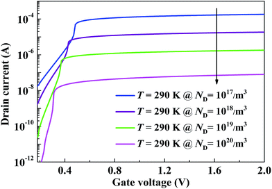 |
| | Fig. 4 Doping concentration effect on the transfer characteristics of the negative capacitance Fe-FET. | |
The influence of temperature on the transfer characteristics of the NC Fe-FET is shown in Fig. 5. Where, the doping concentration is assumed to be 1.0 × 10¹⁹ m−3, and the drain voltage is 0.1 V. In the temperature range from 290 K to 380 K, we can find that the subthreshold characteristics gradually degraded with increasing temperature. That is to say, the subthreshold swing increases from 51 mV dec−1 to 71 mV dec−1. The reason is that the ferroelectric NC effect gradually becomes weak when temperature increases from 290 K to 380 K, resulting in the amplification factor of the silicon surface potential over gate voltage becoming small (see Fig. 3(b)). This result also fits well with the previous result reported by Salvatore.8
 |
| | Fig. 5 Temperature effect on the transfer characteristics of the negative capacitance Fe-FET. | |
Conclusions
In summary, an improved model for the surface potential and drain current in negative capacitance ferroelectric field effect transistors (NC-FeFETs) was presented by introducing the doping concentration. The silicon doping concentration and the temperature effect on the amplification of the silicon surface potential over the gate voltage and the transfer characteristics were investigated. The results indicated that the subthreshold slope can be improved when enhancing the doping concentration, at the cost of decrease in the drive current. When the temperature increases from 290 K to 380 K, the ferroelectric negative capacitance effect gradually becomes weak and the ability of voltage amplification shrinks, which result in the subthreshold swing increasing from 51 mV dec−1 to 71 mV dec−1. It is expected that this investigation may provide some insight into the design and performance improvement for the fast switching and low power dissipation applications of Fe-FETs.
Acknowledgements
This work was financially supported by the National Natural Science Foundation of China (NSFC) (Grant No. 61274107, 51472210 and 61404113).
Notes and references
- S. Salahuddin and S. Datta, Nano Lett., 2008, 8, 405 CrossRef CAS PubMed.
- G. A. Salvatore, D. Bouvet and A. M. Ionescu, in IEDM Tech. Dig., 2008, pp. 1–4 Search PubMed.
- D. Jiménez, E. Miranda and A. Godoy, IEEE Trans. Electron Devices, 2010, 57, 2405 CrossRef.
- A. Cano and D. Jiménez, Appl. Phys. Lett., 2010, 58, 3168 Search PubMed.
- Y. G. Xiao, M. H. Tang, J. C. Li, B. Jiang and J. He, Microelectron. Reliab., 2012, 52, 757 CrossRef CAS.
- A. I. Khan, D. Bhowmik, P. Yu, S. J. Kim, X. Q. Pan, R. Ramesh and S. Salahuddin, Appl. Phys. Lett., 2011, 99, 113501 CrossRef.
- Y. G. Xiao, M. H. Tang, J. C. Li, C. P. Cheng, B. Jiang, H. Q. Cai, Z. H. Tang, X. S. Lv and X. C. Gu, Appl. Phys. Lett., 2012, 100, 083508 CrossRef.
- G. A. Salvatore, A. Rusu and A. M. Ionescu, Appl. Phys. Lett., 2012, 100, 163504 CrossRef.
- W. W. Gao, A. Khan, X. Marti, C. Nelson, C. Serrao, J. Ravichandran, R. Ramesh and S. Salahuddin, Nano Lett., 2014, 14, 5814 CrossRef CAS PubMed.
- D. J. R. Appleby, N. K. Ponon, K. S. K. Kwa, B. Zou, P. K. Petrov, T. Wang, N. M. Alford and A. O'Neill, Nano Lett., 2014, 14, 3864 CrossRef CAS PubMed.
- M. H. Lee, Y.-T. Wei, K.-Y. Chu, J.-J. Huang, C.-W. Chen, C.-C. Cheng, M.-J. Chen, H.-Y. Lee, Y.-S. Chen, L.-H. Lee and M.-J. Tsai, IEEE Electron Device Lett., 2015, 36, 294 CrossRef CAS.
- J. Jo and C. Shin, Curr. Appl. Phys., 2015, 15, 352 CrossRef.
- A. I. Khan, K. Chatterjee, B. Wang, S. Drapcho, L. You, C. Serrao, S. R. Bakaul, R. Ramesh and S. Salahuddin, Nat. Mater., 2015, 14, 182 CrossRef CAS PubMed.
- J. Jo, W. Y. Choi, J.-D. Park, J. W. Shim, H.-Y. Yu and C. Shin, Nano Lett., 2015, 15, 4553 CrossRef CAS PubMed.
- L. D. Landau and I. M. Khalatnikov, Dokl. Akad. Nauk, 1954, 96, 469 Search PubMed.
- V. C. Lo, J. Appl. Phys., 2003, 93, 3353 CrossRef.
- W. Zhang and K. A. Bhattacharya, Acta Mater., 2005, 53, 185 CrossRef CAS.
- K. M. Rabe, C. H. Ahn and J. M. Triscone, Physics of ferroelectrics: A modern perspective, Springer, Berlin, Germany, 2007 Search PubMed.
- S. M. Sze, Physics of semiconductor devices, Wiley, New York, USA, 2nd edn, 1983 Search PubMed.
- Y. Taur and T. H. Ning, Fundamentals of modern VLSI devices, Cambridge Univ Press, Cambridge, UK, 1998 Search PubMed.
|
| This journal is © The Royal Society of Chemistry 2016 |
Click here to see how this site uses Cookies. View our privacy policy here.