
 Open Access Article
 This Open Access Article is licensed under a Creative Commons Attribution-Non Commercial 3.0 Unported Licence
Flexible humidity sensors composed of graphite-like carbon micro-pinecone arrays†
Tomohiko
Nakajima
*,
Takako
Nakamura
and
Tetsuo
Tsuchiya
Advanced Coating Technology Research Center, National Institute of Advanced Industrial Science and Technology, Tsukuba Central 5, 1-1-1 Higashi, Tsukuba, Ibaraki 305-8565, Japan. E-mail: t-nakajima@aist.go.jp; Tel: +81-29-861-6368
First published on 5th October 2016
Abstract
We have prepared flexible graphite-like carbon humidity sensors at room temperature in air. Self-organized carbon micro-pinecone (CMP) arrays consisting of stacks of very thin nanosheets with thicknesses below 5–10 nm and arranged in a pinecone shape were fabricated by KrF laser irradiation of flexible polyimide sheets containing SiO2 nanoparticles of approximately 5 nm in diameter. The Raman spectrum of CMP showed two clear bands, at 1350 cm−1 (D) and 1598 cm−1 (G), indicating a typical graphite-like carbon structure. Temperature simulation of photothermal heating during KrF laser irradiation of the polyimide substrate containing a single SiO2 nanoparticle suggested that the areas surrounding the SiO2 nanoparticle experience a much higher photothermal heating effect than other areas, leading to preferential combustion of carbon near the nanoparticles. This modulation of the photothermal heating temperature is likely strongly related to CMP formation. The obtained CMP arrays showed high sensitivity for humidity when decorated with surface noble metal nanoparticles and Pt-decorated CMP in particular showed very good response and high sensitivity.
Introduction
Carbon nanomaterials of various geometric shapes and crystal forms hold promise for diverse applications such as gas sensors, supercapacitors, catalysts and tribological coatings.1–7 These applications would take advantage of the high tunability of carbon nanomaterial surfaces, and thus there has been significant interest in new approaches to the nanostructuring of carbon nanomaterials into fine nanoparticles,8 nanosheets containing graphite/graphene,9,10 single/multi-walled nanotubes,11,12 nanofibers,13 and nanoflakes.14 Applications in electronic devices would benefit greatly from planar nanostructures that can exploit the covalent bonding capabilities of sp2 hybridized orbitals in graphite-based materials to improve electrical conductivity. Moreover, the identification of new nanostructures is essential for maximizing the properties of new sensing devices by providing platforms amenable to optimum surface modifications.Various chemical vapor deposition methods have been used to fabricate carbon nanomaterials,14,15 of which the laser combustion process (LCP) has recently received significant attention because of its flexible applications. The LCP can fabricate carbon nanostructured membranes by the combustion of an organic substrate surface such as a polyimide sheet.16–19 A self-organized carbon micro-cone (CMC) array consisting of carbon nanoparticles prepared by excimer laser irradiation of polyimide substrates is a well-known example,16,17 and CO2 laser irradiation of polyimide sheets can be used to fabricate porous graphene membranes.18,19 A very important advantage of these LCPs is that patterning of carbon nanomaterial films at room temperature in air is straightforward. This is a significant advantage for the fabrication of carbon nanomaterials for use in devices. Therefore, the discovery of new and varied structural forms of carbon nanomaterials using laser processing is important.
We have studied the effect of the combustion source on the formation of carbon nanostructured membrane formation using excimer laser irradiation at room temperature in air and found that a new carbon micro-pinecone (CMP) array was fabricated by the combustion of polyimide substrates containing very small SiO2 nanoparticles. The obtained CMP arrays were formed by stacking very thin carbon nanosheets. The CMP array nanostructure showed lower sheet electrical resistance than conventional CMC arrays and good humidity sensing properties when the surface was decorated with noble metal nanoparticles.
Experimental procedures
Commercial Pomiran (Arakawa Chemical Industries; thickness: 38 μm) and Kapton (DuPont; thickness: 50 μm) flexible films were used as polyimide source materials. Pomiran is characterized by SiO2 nanoparticles approximately 5 nm in diameter that are uniformly dispersed in the resin.20 Kapton contains no SiO2 nanoparticles in the resin but the surface is coated with a thin layer of SiO2 to prevent the films from sticking to each other. Pomiran and Kapton films were irradiated with a KrF laser (Compex 110, Lambda Physik) at a fluence of 50–200 mJ cm−2 at room temperature in air. Dispersions of Pt, Pd and Au nanoparticles (10 mM; approximately 5 nm in diameter) (Renaissance Energy Research) were spin-coated at 4000 rpm for 10 s on the laser-irradiated polyimide film surfaces to demonstrate their humidity sensing properties. The metal nanoparticle coating procedure was repeated twice and then the films were dried at 100 °C for 30 min.The microscopic morphology and elemental composition of the samples were examined by field-emission scanning electron microscopy (FESEM; SU9000, Hitachi) and energy dispersive X-ray spectrometry (EDS; Genesis, Edax). Raman spectra were collected using a laser Raman spectrometer (NRS 7100, Jasco). X-ray photoemission spectroscopy (XPS) was carried out using an Al Kα source. The electrical resistance (R) was measured using a two-probe geometry under various dry and humidified gases using a digital multimeter (DMM4050, Tektronix). The relative humidity (RH) during measurements was monitored using a humidity temperature meter (Model 725, B&K Precision). The monitoring setup is shown in Fig. S1.†
Temperature variations during laser irradiation can be described by the heat diffusion equation simplified to express one-dimensional heat flow:21–23

Results and discussion
Graphite-like carbon nano-micro sized structures on polyimide sheets
Fig. 1a shows FESEM images of laser-irradiated Pomiran surfaces. The surface begins to carbonize at 50 mJ cm−2; shallow cone-shaped undulations are observed at the surface, but no specific nanostructures are evident. The carbonized surface had a definite self-organized structure similar to that of micro-cone arrays at fluence values above 100 mJ cm−2. The diameter of the base of the arrays was 2–3 μm and the depth of the channels increased with increasing laser fluence. It is noteworthy that the observed micro-cones consisted of stacks (a few micrometers thick) of very thin nanosheets with a thicknesses below 5–10 nm and shaped like a pinecone (Fig. 1b and S2†). We call this self-organized structure a CMP array. CMC array structures have been observed on laser irradiated Kapton polyimide sheets,16,17 as shown in Fig. 1c. These CMC arrays consist of nanoparticulate carbon of approximately 10 nm in diameter, show no other ordered nanostructure, and have base diameters very similar to that of CMP arrays (2–3 μm). A cross-sectional view of CMP arrays prepared using a KrF laser at a fluence of 200 mJ cm−2 shows that the channel depth (cone height) is approximately 2 μm. Thus, the obtained CMP array structure is very unique among structures obtained by the laser irradiation of carbonized polyimide films. | ||
| Fig. 1 (a) FESEM images of the CMP arrays prepared by KrF laser irradiation of Pomiran polyimide films at a fluence of 50, 100, 150 or 200 mJ cm−2. Enlarged views of the FESEM images of the CMP arrays are shown in (b) and of the CMC arrays in (c). (d) A cross-sectional FESEM image of the CMP array irradiated at 200 mJ cm−2. | ||
The Raman spectra of untreated Pomiran and Kapton showed no peaks between 1000–3500 cm−1. In contrast, the CMP and CMC arrays produced by laser irradiation showed characteristic Raman peaks at 1350 cm−1 (CMP) and 1362 cm−1 (CMC) assigned to the D band and corresponding to defects and disordered structure, and at 1598 cm−1 (CMP) and 1612 cm−1 (CMC) assigned to the G band and corresponding to bending of the sp2 bonds in crystalline graphite (Fig. 2a).24,25 The 2D band at around 2700 cm−1 characteristic of graphene26 was not observed in the present carbonized samples produced by nano-second pulsed UV laser irradiation. Therefore, the obtained CMP and CMC arrays consisted of graphite-like carbon. The G band peak position of CMP was slightly shifted to lower wavenumber compared to CMC, indicating fewer crystal imperfections in the graphite. In addition, the G band was somewhat larger than the D band in the CMP arrays (the intensity ratio ID/IG was 0.924), whereas the G band was somewhat smaller than the D band in the CMC arrays (ID/IG = 1.143). These relative band intensities further indicate that the graphite-like carbon in the CMP arrays is more crystalline and has fewer defects arising from the graphite-like carbon nanosheets comprising CMP.
 | ||
| Fig. 2 (a) Raman and (b) XPS spectra of Pomiran and Kapton sheets and the CMP and CMC arrays prepared from each type of polyimide film. | ||
The XPS spectra for Kapton show the Si 2s and 2p peaks prior to laser irradiation, but these peaks are absent in the XPS spectra of the CMC arrays, likely because of laser ablation of the surface SiO2 thin layer during the pyrolytic reaction with the polyimide surface. In contrast, the XPS peaks due to SiO2 were present in the spectra of the CMP arrays, indicating that the dispersed SiO2 nanoparticles remained in the carbonized regions even after laser irradiation (Fig. 2b). Therefore, the differences in the nanostructures of the CMP and CMC arrays result from the original nanoscale compositional distribution of SiO2 in the polyimide films.
The mechanism by which cone array structures form during laser irradiation of polyimide films without SiO2 nanoparticles dispersed in the resin has been studied in previous reports.16,17 In what way does carbonization of polyimide films containing dispersed SiO2 nanoparticles differ? To qualitatively evaluate the effects of SiO2 nanoparticles dispersed in the resin, we calculated the temperature distributions in polyimide and graphite during exposure to a single laser pulse; details of the calculation are provided in the ESI.†Fig. 3a shows the temperature map after a single pulse of laser irradiation onto polyimide. The simulated temperature is considerably above 1000 °C for over 6 μs due to the very small thermal conductivity of polyimide (1.2 mW cm−1 K−1).27 This high temperature would cause rapid carbonization after laser irradiation, as seen in the experimental results (the carbonization temperature of polyimide is around 500–600 °C (ref. 28)). After carbonization, the pulsed temperature increase is much lower than is the case for non-irradiated polyimide due to the very high thermal conductivity of graphite (1.12 W cm−1 K−1).29 At the initial stage of this process, the significant difference in photothermal heating between the polyimide areas and the carbonized areas results in the formation of cone arrays. Silvain et al. speculated that the first carbon nanoparticles produced by laser irradiation could aggregate on the polyimide surface, producing deep channels (cone array formation) as a result of the random distribution of high and low temperature regions.17
 | ||
| Fig. 3 Simulated temperature mapping as a function of depth and time for (a) polyimide and (b) graphite under KrF laser irradiation at 200 mJ cm−2, and the variation in relative temperature with the depth of the SiO2 nanoparticle (d = 15 nm) in (c) polyimide (t = 53 ns) and (d) graphite (t = 45 ns). T and T0 represent the temperatures for models with and without the SiO2 nanoparticle, respectively. | ||
The surface temperature increased to above 600 °C within several tens of nanoseconds and to a depth of several hundred nanometers. In one model, a single SiO2 nanoparticle was introduced into the polyimide film at depths ranging from 0–315 nm, whereas the other model contained no SiO2 nanoparticle. The depth dependence of the relative temperature (T/T0) between the models with (T0) and without (T) a SiO2 nanoparticle 53 ns after the incident pulse is shown in Fig. 3c. The calculated T/T0 clearly shows a 10–20% increase in temperature behind the SiO2 nanoparticle at a depth of 350 nm and a decrease of about 5–10% just above the SiO2 nanoparticle at a depth of approximately 20 nm. This means that polyimide in the vicinity of a SiO2 nanoparticle is at a higher temperature during laser irradiation than polyimide without SiO2 nanoparticles. A photothermal simulation was also conducted for graphite as a model of the polyimide substrate surface after carbonization. A single SiO2 nanoparticle was introduced into the graphite at depths ranging from 0–720 nm; a second model did not contain a SiO2 nanoparticle. The T/T0 after 45 ns (Fig. 3d) shows a 5–10% increase in base temperature compared to the model without the SiO2 nanoparticle, and T/T0 suddenly increases by 1–7% at the top part of the SiO2 nanoparticle. The graphite model used in this calculation has very high thermal conductivity and its density (2.26 g cm−3) is the ideal density for graphite.29 This temperature simulation following carbonization is likely an underestimate since the actual material would have lower thermal conductivity and density. Therefore, these results strongly suggest that the vicinity around the SiO2 nanoparticles likely undergoes much higher photothermal heating than other areas of the graphite sample.
Fig. 4a shows the EDS spectrum and element maps for the CMP arrays. EDS signals were detected for carbon, Si and O. The element maps revealed Si corresponding to SiO2 nanoparticles near the edges of graphite-like carbon nanosheets (ring-shaped aggregations) whereas carbon was homogeneously distributed throughout the cones. Based on the thermal simulations and element maps, we suggest that the CMP arrays form by the following mechanism. The cone arrays grow through the formation of micro-domains comprising aggregated carbon nanoparticles that decrease photothermal heating in their vicinity in the molten polyimide sheet.17 If the polyimide contains SiO2 nanoparticles, the SiO2 nanoparticles aggregate along the solid–liquid interface near the base of the cones, resulting in ring-shaped aggregates. At the moment of SiO2 aggregation, the photothermal heating effect would increase around the aggregated SiO2 nanoparticles, leading to preferential combustion of carbon nearby the SiO2 nanoparticles. Carbon located in areas with fewer SiO2 nanoparticles forms graphite-like carbon nanosheets with residual SiO2 nanoparticles on the surfaces of the nanosheets. This process is repeated during pulsed laser irradiation, resulting in the generation of the CMP arrays. It is difficult to obtain direct evidence to support this proposed mechanism because the phase transformations occur on the order of nano- to microseconds; however, the variation in photothermal heating caused by the presence of the SiO2 nanoparticles and the aggregation of SiO2 nanoparticles must affect CMP formation. It is very interesting that this new nano/micro-sized carbon structure was realized just by introducing nanomaterials into the carbonized sources and applying simple atmospheric laser irradiation.
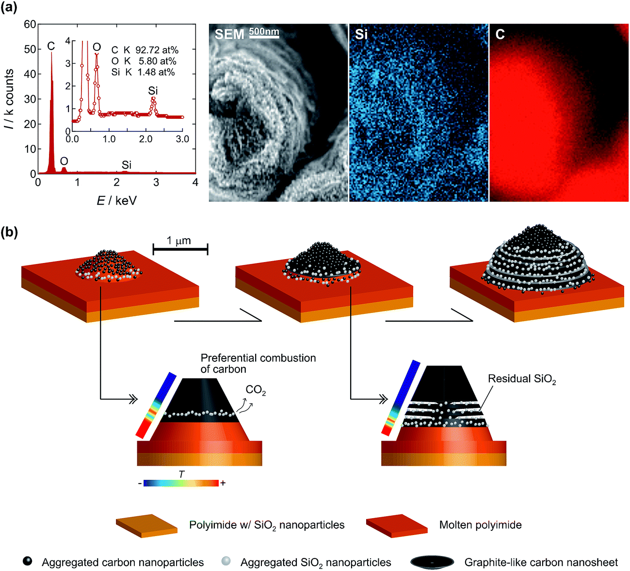 | ||
| Fig. 4 (a) EDS spectrum and element maps for Si and C in CMP. (b) Schematic illustration of a CMP growth model during pulsed laser irradiation. | ||
Humidity sensing properties of CMP and CMC arrays
We studied the humidity sensing properties of the CMP and CMC arrays. Sensing was enhanced by decorating the surfaces of the CMP and CMC arrays with noble metal (Pt, Pd or Au) nanoparticles. Fig. 5 shows FESEM images of Pt-decorated CMP and CMC (CMP–Pt and CMC–Pt); CMP–Pt and CMC–Pt were prepared by KrF laser irradiation at 200 mJ cm−2, followed by spin-coating of a Pt dispersion. Pt nanoparticles were observed on the surfaces of the carbon nanosheets of CMP–Pt and on the carbon nanoparticles in CMC–Pt. The size of each Pt nanoparticle size was approximately 5–10 nm, similar to the size of the original source Pt nanoparticles. | ||
| Fig. 5 FESEM images of the cone surface of (a) CMP–Pt and (b) CMC–Pt arrays. | ||
Fig. 6a and S3† shows a 3 mm square CMP–Pt humidity sensor prepared using KrF laser irradiation at a fluence of 200 mJ cm−2 through a photomask and flanked by two silver electrodes fabricated by silver nanoparticle ink deposition. Various CMP and CMC sensors with the same configuration and decorated or not decorated with metal nanoparticles were prepared. Sensors with metal nanoparticles were designated CMP–M and CMC–M (M: Pt, Pd and Au). The prepared sensors were placed in a reaction chamber (Fig. S1†) and the response of R under a flow of dry or humidified N2 was examined at room temperature. The relative humidity (RH) was concurrently measured using a commercial humidity sensor. CMP had a half sheet resistance (RS) of 15.7 kΩ sq−1 at 0% RH and CMC had an RS of 31.6 kΩ sq−1 at 0% RH; these differences reflect the merit of graphite-like carbon nanosheets for better electrical conductivity (Fig. 6b). Fig. 6c shows the R variations (R/R0: R0 represents the R at 0 s) of CMP and CMC as a function of time. The dry N2 gas flow was changed to 90% RH N2 from 30 s to 210 s, then was changed back to dry N2 gas. The R/R0 of CMP and CMC increased during the humid N2 gas flow and dropped following the restart of dry N2 gas flow. This R increase under a humidified atmosphere is due to adsorbed water molecules on the surface of the carbon nanosheets donating electrons to the valence band of carbon, resulting in an increase in electrical resistance due to the lower hole concentration.30 The sensitivity (S) of the arrays to RH is defined as S/% = (ΔR/R0)/Δ(RH%) × 100. In the absence of surface metal nanoparticles, the sensitivity of CMC was 0.011% and 0.008% for CMP (Fig. 6b). Moreover, the response curves did not follow the reference humidity sensing curve, especially after the restart of dry N2 gas flow.
 | ||
| Fig. 6 (a) The fabricated CMP–Pt humidity sensor. (b) The RS and S of CMP, CMP–M, CMC and CMC–M. The time course of R/R0 for (c) CMP and CMC, (d) CMC with/without surface metal nanoparticles and (e) CMP with/without surface metal nanoparticles. The dotted line represents the RH curve as monitored using a commercial humidity sensor. In the time course measurements, the gas flow was changed as follows: dry N2 (0–30 s) – humidified N2 (30–210 s) – dry N2 (210–360 s). | ||
In contrast, decoration of the array surface with metal nanoparticles greatly improved S (Fig. 6b). The presence of Pd, Pt or Au nanoparticles on CMC–M increased R/R0 354% (S = 0.041%), 299% (S = 0.034%) and 276% (S = 0.032%), respectively, compared to CMC without the metal nanoparticles (Fig. 6c). However, the response curves still did not follow the actual humidity variation (Fig. 6d and S4†). Fig. 6e shows the time dependence of R/R0 for CMP–M. The presence of surface Pd and Pt nanoparticles in particular resulted in improved R/R0 (S) values. CMP–Pd, CMP–Pt and CMP–Au exhibited significantly increased R/R0 values of 1195% (S = 0.094%), 772% (S = 0.061%) and 345% (S = 0.027%), respectively, compared to CMP without the corresponding nanoparticles (Fig. 6b and e). In addition, the humidity response of CMP–Pt was in fairly good agreement with the actual humidity variation (Fig. 6e and S5†), while the S value of CMP–Pd was 54% better than that of CMP–Pt.
Fig. 7a and b show the R/R0 variations for humidified/dry hydrogen and oxygen atmospheres. Flowing humidified H2/Ar and O2 over the arrays resulted in an increase in R/R0, similar to that observed with humidified N2 flow, whereas R/R0 was essentially unresponsive to dry gases, indicating that CMP–Pt exhibited a selective response to humidity. The RH dependence of R/R0 for CMP–Pt at 20 °C is shown in Fig. 7c. The R/R0 plot exhibited an almost linear increase over a wide range of RH values from 0% to 90%. However, despite the good response and very low noise obtained with the CMP–Pt sensor, two issues should be addressed: (1) the temperature dependence of the sensor and (2) the bending of the sensor. The temperature dependence resulted in an approximately 2% decrease in R in the range between 20–80 °C (Fig. 7d) and the bending test resulted in an R variation of around 1.5–2.0% (Fig. 7e). The temperature dependence of R could be ignored if the S were sufficiently increased. A further increase in S might be achieved by optimally connecting the graphite-like carbon nanosheets within the array (which would also lower the R variation in the bending tests) and optimizing the metal nanoparticles on the nanosheet surface.
 | ||
| Fig. 7 The time course of R/R0 for CMP–Pt in (a) dry and humidified H2/Ar and (b) dry and humidified O2. The gas flow was changed as follows: (a) dry N2 (0–30 s) – dry or humidified H2/Ar (30–210 s) – dry N2 (210–360 s) and (b) dry N2 (0–30 s) – dry or humidified O2 (30–210 s) – dry N2 (210–360 s). (c) RH (T = 20 °C) and (d) temperature (RH = 5%) dependences of the relative R for CMP–Pt. (e) Time course of the relative R at RH = 35% and 20 °C with continuous bending action for CMP–Pt. The bending radius was 3 cm. | ||
Conclusions
We have prepared self-organized CMP arrays from polyimide sheets containing SiO2 nanoparticles approximately 5 nm in diameter. The arrays were generated by stacks (a few micrometers thick) of very thin nanosheets with thicknesses below 5–10 nm in a pinecone-like structure using KrF laser irradiation at room temperature in air. The Raman spectrum of CMP clearly showed two bands, at 1350 cm−1 (D) and 1598 cm−1 (G), indicating typical graphite-like carbon formation. Temperature simulation of photothermal heating during KrF laser irradiation of polyimide substrate containing a SiO2 nanoparticle suggests that the area surrounding the SiO2 nanoparticle experiences a much higher photothermal heating effect than the other parts of the substrate, leading to preferential combustion of carbon near the nanoparticle. This modulation of the photothermal heating temperature is likely a major determinant of CMP formation. The obtained CMP array showed high sensitivity to humidity when its surface was decorated with noble metal nanoparticles. CMP–Pt in particular showed very good response to high sensitivity. We therefore achieved the fabrication of a flexible humidity sensor by using a very straightforward process at room temperature in air.Notes and references
- M. Gautam and A. H. Jayatissa, Mater. Sci. Eng., C, 2011, 31, 1405 CrossRef CAS.
- M. Penza, R. Rossi, M. Alvisi, D. Suriano and E. Serra, Thin Solid Films, 2011, 520, 959 CrossRef CAS.
- E. Frackowiak and F. Béguin, Carbon, 2001, 39, 937 CrossRef CAS.
- M. Sevilla and R. Mokaya, Energy Environ. Sci., 2014, 7, 1250 CAS.
- Y. Zhu, S. Murali, M. D. Stoller, K. J. Ganesh, W. Cai, P. J. Ferreira, A. Pirkle, R. M. Wallace, K. A. Cychosz, M. Thommes, D. Su, E. A. Stach and R. S. Ruoff, Science, 2011, 332, 1537 CrossRef CAS PubMed.
- L.-W. Zhang, H.-B. Fu and Y.-F. Zhu, Adv. Funct. Mater., 2008, 18, 2180 CrossRef CAS.
- A. Erdemir and C. Donnet, J. Phys. D: Appl. Phys., 2006, 39, R311 CrossRef CAS.
- S. Y. Lim, W. Shen and Z. Gao, Chem. Soc. Rev., 2015, 44, 362 RSC.
- T. Hayashi, S. Hirono, M. Tomita and S. Umemura, Nature, 1996, 381, 772 CrossRef.
- K. S. Novoselov, A. K. Geim, S. V. Morozov, D. Jiang, Y. Zhang, S. V. Dubonos, I. V. Grigorieva and A. A. Firsov, Science, 2004, 306, 666 CrossRef CAS PubMed.
- A. C. Dillon, K. M. Jones, T. A. Bekkedahl, C. H. Kiang, D. S. Bethune and M. J. Heben, Nature, 1997, 386, 377 CrossRef CAS.
- R. Martel, T. Schmidt, H. R. Shea, T. Hertel and Ph. Avouris, Appl. Phys. Lett., 1998, 73, 2447 CrossRef CAS.
- A. V. Melechko, V. I. Merkulov, T. E. McKnight, M. A. Guillorn, K. L. Klein, D. H. Lowndes and M. L. Simpson, J. Appl. Phys., 2005, 97, 041310 CrossRef.
- N. G. Shang, F. C. K. Au, X. M. Meng, C. S. Lee, I. Bello and S. T. Lee, Chem. Phys. Lett., 2002, 358, 187 CrossRef CAS.
- A. M. Cassell, J. A. Raymakers, J. Kong and H. Dai, J. Phys. Chem. B, 1999, 103, 6484 CrossRef CAS.
- D. J. Krajnovich and J. E. Vázquez, J. Appl. Phys., 1993, 73, 3001 CrossRef CAS.
- J.-F. Silvain, H. Niino, S. Ono, S. Nakaoka and A. Yabe, Appl. Surf. Sci., 1999, 141, 25 CrossRef CAS.
- J. Lin, Z. Peng, Y. Liu, F. Ruiz-Zepeda, R. Ye, E. L. G. Samuel, M. J. Yacaman, B. I. Yakobson and J. M. Tour, Nat. Commun., 2014, 5, 5714 CrossRef CAS PubMed.
- Z. Peng, J. Liu, R. Ye, E. L. G. Samuel and J. M. Tour, ACS Appl. Mater. Interfaces, 2015, 7, 3414 CAS.
- http://www.arakawachem.co.jp/en/business/photo/02.html .
- D. Bäuerle, Laser Processing and Chemistry, Springer-Verlag, Berlin, Heidelberg, New York, 2000 Search PubMed.
- T. Nakajima, K. Shinoda and T. Tsuchiya, Chem. Soc. Rev., 2014, 43, 2027 RSC.
- T. Nakajima, T. Tsuchiya, M. Ichihara, H. Nagai and T. Kumagai, Appl. Phys. Express, 2009, 2, 023001 CrossRef.
- Y. Liu, M. Zhou, Y. Hu, H. Qian, J. Chen and X. Hu, CrystEngComm, 2012, 13, 4507 RSC.
- L. Marcinauskas, A. Grigonis, P. Valatkevicius and A. Medvid, Appl. Surf. Sci., 2012, 261, 488 CrossRef CAS.
- A. C. Ferrari, J. C. Meyer, V. Scardaci, C. Casiraghi, M. Lazzeri, F. Mauri, S. Piscanec, D. Jiang, K. S. Novoselov, S. Roth and A. K. Geim, Phys. Rev. Lett., 2006, 97, 187401 CrossRef CAS PubMed.
- http://www.dupont.com/content/dam/dupont/products-and-services/membranes-and-films/polyimde-films/documents/DEC-Kapton-summary-of-properties.pdf .
- J. Su and A. C. Lua, J. Membr. Sci., 2007, 305, 263 CrossRef CAS.
- https://www.entegris.com/resources/assets/6205-7329-0513.pdf .
- J. Chu, X. Peng, P. Feng, Y. Sheng and J. Zhang, Sens. Actuators, B, 2013, 178, 508 CrossRef CAS.
Footnote |
| † Electronic supplementary information (ESI) available. See DOI: 10.1039/c6ra21902k |
| This journal is © The Royal Society of Chemistry 2016 |