The effect of the surface energy and structure of the SiC substrate on epitaxial graphene growth

Li Suna, Xiufang Chen*a, Wancheng Yua, Honggang Sun*b, Xian Zhao*a, Xiangang Xua, Fan Yuc and Yunfeng Liuc
aState Key Laboratory of Crystal Materials, Shandong University, Jinan, 250199, China. E-mail: cxiufang365@126.com; sunhg@sdu.edu.cn; zhaoxian@sdu.edu.cn; Fax: +86-531-88364864; Tel: +86-531-88366330
bSchool of Mechanical, Electrical & Information Engineering, Shandong University, Weihai, 264209, China
cInstitute of Optics and Electronics, Chinese Academy of Science, Chengdu, 610209, China

Received 31st August 2016 , Accepted 19th October 2016

First published on 19th October 2016


Abstract

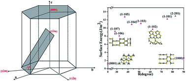
The exposed surfaces of the SiC substrate have a great influence on the epitaxial graphene growth and morphology and thus influence the properties of graphene-based microelectronic devices. In this work, the surface structures of the SiC substrate were determined by first principle theoretical calculations. Calculated surface energies suggested that the SiC step structure, forming on the H2 etching procedure, would be reconstructed and self-ordering to expose the (1−106) facet. The inclined angle of 33.23° of the vicinal surface observed by Atomic Force Microscope (AFM) demonstrated the calculated results. The relationship between graphene growth and the surface Si–C bonding strength was revealed by calculating the formation energies of Si vacancies. Combined the calculated formation energies with Raman analysis, we concluded that the nucleation of graphene growth on the SiC substrate preferred to occur at step (1−106) surface rather than terrace (0001) surface. In addition, the single Si atom would facilitate the assembling of surface C atoms. The present theoretical and experimental work is helpful to optimize the technology of epitaxial graphene growth on the SiC substrate.


1 Introduction

Since graphene was successfully fabricated in the year 2004,1 it has been considered as a promising material for applications in optical, chemical and semiconductor areas due to its unique band structure, extremely high Young modulus, thermal conductivity, and carrier mobility.2 Compared with graphite nanoplatelets (GNPs), who afford super diameter/thickness ratios and good compatibility with polymeric matrices, graphene shows more outstanding properties in the semiconductor area.3–6 Large-scale preparation of high-quality graphene is beneficial to its applications.7 Therefore, the preparation of graphene has been attracting extensive research. In recent years, four methods have been developed for making larger quantities of the graphene material: micromechanical exfoliation, chemical oxidation–reduction, chemical vapor deposition (CVD) on metal surfaces and epitaxial graphene by thermal decomposition of SiC.1,8–15 Hereinto, the growth method by thermal decomposition of SiC offers a high quality graphene material in semiconductor devices areas.16 Especially, SiC has proven to be one of the most promising semiconductors for device applications owing to its extraordinary properties, such as wide band gap, high breakdown electric field and excellent physical stability under extreme conditions. Therefore, the graphene and the built-in electronic grade SiC substrate can be directly applied to electronic device without destructive transferring procedure,17,18 which reserves the integrity of graphene to the most extend. In that, the epitaxial method on SiC substrate is an attractive route on graphene-based device areas.

The common epitaxial graphene growth craft can be divided into three steps: pretreating–annealing–cooling.3,19 The pretreat procedure is typically executed by H2 etching, leaving behind smoothen and broaden SiC surfaces.20 During the step bunching process, the SiC terrace and step rearrange to acquire equilibrium state as temperature escalating.21,22 A set number of studies have shown the influence of SiC substrate surface on epitaxial graphene, both on graphene structure, pit formation and electronic properties.23–26 As it has been reported by Magna, the presence of a monolayer/bilayer or monolayer/few layers lateral junction could result in a decrease of the conductance.27 Oliveira pointed out that the geometry configuration would attain a surface energy minimum state when H2 etching process was exposed to a certain temperature.28 As a result, the subsequent graphene growth, following the original pattern of former etched surface, is accompanied with a more regular morphology. However, the mechanism of the exposed terrace and step surface rearrange during epitaxial process is still unclear due to the lack researches about the SiC surface structures. Therefore, new jobs are needed to further understand the surface characteristic of the SiC substrate.

Surface energy is one of the important information for the crystal surface structures, both in bulk single crystal growth29 and the nanoparticle morphology.30 Based on Wulff's theory,31 the crystal usually exposes those surfaces with a relative lower surface energy. The surface with higher surface energy may undergo a larger reconstruction during the surface growth or treatment, which will influence the preferential sites of epitaxial growth. Theoretical calculations have been used to analyze the surface structure and the surface energy of crystals.32,33 Unfortunately, till now, there is a lack of the theoretical data on the SiC surface energies since the existing obstacles are academically inevitable. In the past, the slab model was successfully used to calculate surface energy.34 However, it is difficult for the slab model to calculate accurate surface energies of polar SiC faces due to the electrostatic potential between the top surface and the bottom surface. Although enough thickness of slab will suppress the polar effect, more computational time is needed.35 Shiraishi proposed that a slab model completely terminated by H atoms can represent authentic quality of a set of polar surfaces, and economize the computational time as well.36,37 Especially, the wedge model, consist of the required face and the known faces, was also considered as an effective method to achieve the surface energies of the polar faces.38,39 In addition, the graphene growth on the pretreating SiC substrate goes through the sublimation of Si atoms and the assembling of remaining C atoms, which are correlated with the SiC surface structures. Therefore, it is necessary to study the effect of the SiC surface structures on the graphene growth by appropriate theoretical methods.

In the present paper, first principle calculations combined with experimental measurements were employed to study the surface structures of the pretreating SiC substrate. Two main contributions were shown in the present work. One focused on the revelation of the stable surface structures of the H2 pretreating SiC substrate by the combining theoretical calculations and experimental measurements, the other is the exploring of the mechanism of the graphene nucleation and growth by calculating the formation energies of the surface Si vacancies. It is expected that this study would offer a clear understanding on interaction between the graphene growth and the SiC substrate.

2 Theoretical and experimental parameters

2.1 Theoretical parameters

All calculations were performed using Cambridge Sequential Total Energy Package (CASTEP) in the frame work of the first-principles density functional theory (DFT). The generalized gradient approximation (GGA) with the Perdew–Burke–Ernzerhof (PBE) functional40 was used for the exchange and correlation interactions. The ultrasoft pseudopotential was used to deal with the core electrons and the valence atomic configurations are 2s22p2 for C, 3s23p2 for Si. The hexagonal 4H-SiC crystal cell with P63mc space group was completely relaxed in the present work. To achieve the accurate lattice parameters, the plane wave cutoff was set as 340.0 eV, and the k-point of 9 × 9 × 2 was used for the relaxation using the Monkhorst–Pack scheme.41 The present parameters were also used in other work.42–44 All forces on atoms were converged to less than 0.03 eV Å−1; the maximum ionic displacement was within 0.001 Å. and the total stress tensor was reduced to the order of 0.05 GPa. The optimized lattice parameters were a = 3.086 Å and c = 10.094 Å, in good agreement with the experimental value where a = 3.081 Å, and c = 10.080 Å from X-ray diffraction measurement.45

The polar (0001) surface energy was calculated through a slab model, which consisted of (2 × 2) unit cell with six Si–C bilayers and a 15 Å vacuum layer. The surface unsaturated atoms were compensated with H atom to depress the polar effect. For the non-polar (1000) face, (2 × 1) unit cell with four Si–C bilayers and a 15 Å vacuum layer was utilized to calculate the surface energy. To calculate the surface energy of (1−10n) faces, the wedge models were constructed by (0001), (1000) and (1−10n) faces. All surface models were constructed by the optimized 4H-SiC crystal cell. The above three models were fully relaxed before surface energy calculations using k-points of 5 × 5 × 1, 4 × 2 × 1, and 5 × 1 × 1, respectively. The detailed convergence tests were given in the ESI.

2.2 Synthesis of graphene

The substrates used in this work were nominally on-axis 4H-SiC, with the miscut angle tolerances within ±0.20°, made by State Key Laboratory of Crystal Materials, Shandong University. The Si-terminated face of the substrate was processed by chemical mechanical polishing (CMP). Then the substrate was cleaned by sulfuric acid/hydrogen peroxide, ammonium hydroxide/hydrogen peroxide, hydrochloric acid/hydrogen peroxide, hydrofluoric acid and deionized water consecutively. After CMP treatment, the Si-terminated face of substrate showed atomic-scale steps, and its root mean square (RMS) roughness was less than 0.5 nm. The 3-inch SiC wafer was cut into 10 mm × 10 mm tablets for the convenience of subsequent growth and characterization. The graphene growth method was same as that described elsewhere.28 Before growth, the SiC substrate was etched in H2 flow at 1600 °C for 20 minutes. Then, the sample was annealed at 1600 °C for an hour under Ar atmosphere (grade 5.0). During the annealing treatment, the pressure of growth chamber was kept at 900 mbar.

2.3 Characterization

The graphene surface morphology was investigated by AFM (Bruker Dimension Icon) with a spatial resolution of 1 nm. The sample was scanned in ScanAsyst mode. Kelvin Potential Force Microscope (KPFM) was used to character the graphene layer divergence. Graphene quality and layer number were characterized by a LabRAM HR800 confocal Raman spectroscopy in back scattering configuration with a 532 nm laser for excitation. The 100× objective (spot size: 1 μm) with the numerical of aperture 0.90 was used. The laser power was estimated to be 15 mW through the lens, making sure the surface graphene was not destroyed. The lateral resolution is about 1.5 cm−1 with a 600 diffraction grating.

The alignment precision for AFM and Raman analysis was guaranteed by a tracking method. Before epitaxial growth, nine positions have been labeled by the marking machine on the (000−1) face in a 10 mm × 10 mm area. These nine spots equally distributed on the whole sample. When one sample was taken out from the furnace, the surface morphology was characterized by AFM at first. Nine fixed points were estimated each time. After AFM estimation, Raman spectra were collected in these nine positions.

3 Results and discussion

3.1 Surface energy

The (0001) Si-terminated surface of the SiC substrate will reconstruct to reform a stable surface structure due to the H2 etching of the pretreat procedure. Gibbs pointed out that the crystal morphology is formatted as the result of reducing the total free energy, that is image file: c6ra21858j-t1.tif. The Wulff's theorem notes the growth rate are proportional to their surface free energies per unit area, σiRi. This means that the faces with high surface energies tend to have a faster growth rate and disappear during growth procedure. As shown in Fig. 1a, the surface of the pretreated SiC substrate consists of flat terraces and gradient steps. The terrace is contributed to (0001) face of SiC, while the step is identified as (1−10n) faces as shown in Fig. 1b. Therefore, the surface energies of (1−10n) faces are necessary to determine the pretreated surface structure. For the nonpolar faces, the top and bottom surfaces are exactly the same. So the surface energy σsurf can be calculated as below:
 
image file: c6ra21858j-t2.tif(1)
Where Eslab and Ebulk represent for the total energy of the constructed slab model and the SiC bulk crystal, respectively, and A is the area of the slab model. However, the model is difficult to calculate the surface energies of polar (1−10n) faces due to the electrostatic potential between the top surface and the bottom surface in the slab. In the present work, the wedge models as shown in Fig. 1c are used to calculate the surface energies and achieve the optimized structures of polar (1−10n) faces. The below formula gives the general energy expression of SiC wedge model,
 
σ(1−10n) + σ(0001) + σ(1000) = EtotalnSiμSinCμCnHμH. (2)

image file: c6ra21858j-f1.tif
Fig. 1 (a) A side view of the pretreated SiC substrate, and (b) the direction in 4H-SiC polytype, and (c) the constructed typical wedge model in this paper. The colors of C and Si atoms are gray and yellow, respectively.

Hereinto, σ(0001) and σ(1000) are calculated by formula (1). The (0001) surface structure consists of alternated C and Si atoms, and the Si-terminated face is used according to the experiment. Etotal is the total energy of the SiC wedge model. nSi, nC, nH and μSi, μC, μH represent for the atom number and potentials of Si, C, and H element species in the wedge model, respectively. The H atoms are introduced to compensate the dangling bonds of the wedge model. According to the calculation described above, larger surface energy means more unstable surface structure. Surface energies σ(1−10n) are calculated when n equals to 1/2, 1, 2, 3, 4, 5, 6, and 7, respectively. For the typical terrace-step arrangement on the SiC substrate, the relevance between the facets inclined angle θ and the plane index n by the equation,

 
image file: c6ra21858j-t3.tif(3)
Where a and c are the lattice parameters of the 4H-SiC single crystal. In the present work, the calculated value of a and c are 3.086 and 10.094 Å, respectively. The calculated surface energies are listed in Fig. 2. It can be seen that as n increases from 1/2 to 2, surface free energy decreases. The declined angle θ of the (1−102) face equals to 62.11°. As the declined angle becomes much lower, the surface energy goes up in fluctuation. When it comes to (1−106) face, here is a sharply decrease, where θ is 32.20°. Continuously, the surface energy displays an upward trend when θ reaches 28.36°. Interestingly, we also found that the surface free energy of the (1−102) face and (1−107) face, whose angles are added up to 90°, are almost in the same number. The phenomenon should be driven by the periodicity inside crystal structure. The present calculations suggest that the surfaces of pretreated SiC substrate mainly consist of (0001) and (1−106) faces.


image file: c6ra21858j-f2.tif
Fig. 2 The calculated surface energies for the different SiC surface in the present work.

Aiming at verifying the surface energy calculations, experiments were carried out by epitaxial graphene on SiC (0001) face. For the pretreated SiC substrate, Fig. 3a displays the AFM image around the step area in a quite exquisite scale of about 150 nm × 150 nm. Nakajima's illustration reveals that the nearly straight structure on the step edge, which results from the step motion on the progress of H2 etching, was parallel to [11−20] direction.22 On the other hand, the facets are proved to be the (1−10n) planes by this feature. Fig. 3b shows the height fluctuation across the step marked by the white line in Fig. 3a. Upper and lower terrace were flat enough to be viewed as horizontal to the width axis, in the average height of −4.6322 nm and 4.5874 nm, respectively. A negative height is reasonable because AFM height values are given by comparison with the total image. For the sloping region, the tangent line equation of center point (coordinates: 37.62564, −0.9464), which can furthest reflect the points trend, is estimated to be y = 0.655x − 25.5908. Then, the lateral view of the step arrangement consists of three lines: tangent, highest and lowest lines. Therefore, the inclined angle of the step is about 33.23°, which is indeed close to the (1−106) face of SiC substrate according to the formula (3). The result is agreement with above surface energy calculations and is also consistent with the observation of the cross-sectional transmission electron microscope in previous research.46 The surface characteristic of the pretreated SiC substrate will affect the graphene nucleation and growth in the next procedure.


image file: c6ra21858j-f3.tif
Fig. 3 (a) The morphology on the step edge estimated in 150 nm × 150 nm, and (b) the height fluctuation near the white line marked in (a). These two lateral red lines represent upper and lower terrace, while the slope line stands for the facets area.

3.2 Surface structures and graphene nucleation

The basic principle of graphene growth on SiC substrate is the sublimation of Si atoms and the reconstructing of remaining C atoms. The strength of the surface Si–C bonds is one of the determinate factors for graphene growth on SiC substrate. Fig. 4a and b give the (0001) and (1−106) surface structures. For the Si-terminated (0001) surface, the surface Si atoms are three coordinated and the Si–C bond length of about 1.883 Å is slightly longer than 1.880 Å in the bulk. For the (1−106) surface, both the C atoms and the Si atoms are exposed with much longer Si–C bond lengths of about 1.904–2.001 Å. The structures suggest that the Si–C bonds of the (1−106) surface are weaker than that of the (0001) surface, and the more open atom arrangement may result in fewer obstacles during the Si sublimation procedure. Furthermore, the formation energies (Ef) of the surfaces Si vacancies (VSi) are calculated to study the sublimation of Si atoms according to the followed formula,
 
Ef = EV + SiEp. (4)
EV and Ep represent the energies of the surfaces with and without Si vacancies, respectively. n are the number of the removal Si atoms. In the whole, the VSi formation energies of the (1−106) surface are smaller than that of the (0001) surface as shown in Table 1. The result indicates that the stronger interaction between Si atoms and C atoms on the (0001) surface and the graphene nucleation prefers on the (1−106) surface.

image file: c6ra21858j-f4.tif
Fig. 4 The SiC perfect and defect surface structures of (a) (0001), and (b) (1−106) faces. The surface and subsurface atoms are labeled in the figure using Sis, Cs, and Sisur, Csur. The proportion of the surface Si vacancy is labeled as Vn/4Si.
Table 1 The VSi formation energies of the (1−106) and (0001) surfaces. The V1/4Si, V2/4Si, V3/4Si, and V4/4Si represent the proportion of the surface Si vacancies, and VsubSi represents the subsurface Si vacancy
SiC surface Formation energy/eV
V1/4Si V2/4Si V3/4Si V4/4Si VsubSi
(1−106) 6.505 6.409 5.886 4.065 3.875
(0001) 13.799 14.080 7.523 22.943 26.446


Fig. 4 also shows the surface structures with different Si vacancies, which gives the Si–C bond lengths of about 1.872–2.000 Å and 1.844–1.847 Å for the (1−106) and the (0001) surface, respectively. The calculated Ef of VSi on the (1−106) surface turns to be lower after the sublimation of Si atoms, which is contributed to the significant reconstruction due to the large free surface structures. However, the surface energies of the (0001) surface become higher and higher as the result of the stronger surface Si–C bonds. In other words, a higher temperature is needed to obtain large size graphene on the terrace area of SiC substrate during the annealing procedure. For the (1−106) surface, the C–C bonds are formed with four Si vacancies as shown in Fig. 4b. Especially, the C atoms on the subsurface are exposed due to the removal of the surface Si atoms. The calculated Ef of the subsurface Si vacancy indicates that the removal of the (1−106) subsurface Si atom is still easier than that on the (0001) surface. Therefore, it can be conclude that the growing graphene on the (1−106) surface will be thicker than that on (0001) surface. The result also suggests that an open structure of the SiC substrate is more favorable for graphene growth. The calculated Ef has a large drop for the third Si vacancy on the (0001) surface, which is contributed to the significant surface reconstruction. As shown in Fig. 4a, the C atoms spontaneously assemble around the surface with a single Si atom on it, while the spontaneous nucleating does not occur for surface with only C atoms. This means that an appropriate Si amount is in favor of epitaxial graphene growth on SiC substrate.

Moreover, when removing four Si atoms on the (1−106) surface, as shown in Fig. 5a, the surface layer begins to delaminate from the substrate with the largest distance about 3.458 Å. However, for the (0001) surface with four Si vacancies, the surface C layer is still strangely bound with the substrate Si atoms with the Si–C bond length of 1.943 Å as shown in Fig. 5b. The results suggest that a C buffer layer may present on the planar SiC (0001) face rather than on the step (1−106) face during the epitaxial graphene growth on SiC substrate. This conclusion is agreement with the Magna's results, which notes the formation of tetrahedral bonds between the Si atom at the SiC (0001) surface and the C monolayer drives the formation of the C buffer layer.42,47 The Raman characterization was utilized to validate the observation from the structure. As it is explained by Seyller,48 the buffer layer structure leads to a non-negligible signal around G peak in the Raman spectrum. Fig. 5c shows a comparison of Raman spectra collected on step edge and terrace area, respectively. In order to eliminate the SiC substrate influence on the G peak, the spectrum of a clean SiC sample has been subtracted from that of epitaxial graphene sample. The step edge displays a totally symmetric G peak. Meanwhile, the asymmetric peak of terrace can be fitted by GB peak and G peak. The result indicates that the buffer layer appears on (0001) polar face rather than on the (1−106) facet, which is also agreement with the present theoretical calculations and Magna's work. The reason for the disappearance of buffer layer on (1−106) facet, whether buffer layer couldn't form at first or it delaminated during the growth procedure, needs further discussion.


image file: c6ra21858j-f5.tif
Fig. 5 The side views of (a) (0001), and (b) (1−106) SiC surface structures with four Si vacancies, and (c) the Raman spectrum around G peak for step edge and terrace.

The morphology and Raman mapping spectra of graphene epitaxial on SiC substrate are displayed in Fig. 6 to study the nucleation mechanism. Fig. 6a is the typical morphology of the epitaxial graphene. The left-bottom inset of Fig. 6a shows the zoom in image of KPFM near a step. It needs to be illustrated that the contact potential deference image were got with the sample being grounded. Thus compared with terrace, higher potential in dark color shows that there are more graphene layers.49 It has also been reported that by contrast to terrace, the step edge area was more disordered and had more wrinkles in some places, which resulted from more carbon layers.50 Fig. 6b gives a Raman mapping spectrum with 5.5 μm × 5.5 μm size for the marked white square area. Every single spot area is 0.5 μm × 0.5 μm. It can be seen that the step edge region exhibits brighter color with the full-width at haft-maximum (FWHM) around 60 cm−1, while the color of terrace region is much darker with the number around 44 cm−1. In terms of the layer equation FWHM (2D) = −45(1/N) + 88 cm−1 proposed by Lee,51 the graphene on step edge region was calculated to be 2–3 layers, while terrace region was only 1 layer. Fig. 6c displays the typical spectra extracted from the Raman mapping image. It is obvious that the 2D peak of step edge is much broader than that of terrace. Additionally, two insets show the Lorentz fit of 2D peak of terrace and step edge areas, respectively. For the Raman spectra collected on the terrace area, 2D peak can be fitted by a single peak, while the 2D peak need to be fitted by four peaks on the step edge area. That means more graphene layers were formed on step edge. Fig. 6d denotes 18 Raman spectra extracted from 6 samples on the step edge and terrace area, respectively. The step edge area owns a high average FWHM than that on terrace. This statistic data verifies the repeatability and representativeness of the present work.


image file: c6ra21858j-f6.tif
Fig. 6 (a) AFM result in the area of 40 μm × 40 μm and the KPFM around the white square, (b) Raman mapping result for the white square, (c) the representative Raman spectra estimated on the terrace and step edge area, respectively, and (d) the statistic Raman spectra collected from six samples.

The experimental observation is in agreement with our theoretical calculations. Combing the calculated and experimental results, the conclusion on graphene formation can be drawn. Firstly, Si atoms on vicinal faces sublime, and provide for the nucleation site. Then graphene grows over the terrace region above the step. Finally, the SiC substrate is totally covered by graphene layers. The atom arrangement difference and nucleation priority often results in the in-homogenous layer distribution on vicinal and Si-terminated faces. The hypothesis proposed in present work is consistent with what was observed by Norimatsu.52,53

4 Conclusion

By applying the different surface models, the surface energies were calculated to determine the expose faces of the SiC substrate. The calculated results indicated that the terrace and step structures induced by H2 etching consisted of (0001) and (1−106) faces, respectively. The further theoretical and experimental studies indicated that the vicinal surface was graphene nucleation priority site. The remaining Si atom on the SiC substrate had a positive influence on the assembling of surface C atoms. This research gave a basic understanding about the effect of the SiC surface energy and structure on epitaxial graphene growth.

Acknowledgements

This work is supported by the National Natural Science Foundation of China (Grant No. 513230013, 51402169 and 51502076), the Fundamental Research Funds for Natural Science of Shandong University (Grant No. 2014QY005), the Shandong Provincial Natural Science Foundation, China (Grant No. ZR2014BP005), and the China Postdoctoral Science Foundation (Grant No. 2013M530322). The numerical calculations in this paper have been done on the supercomputing system in the Supercomputing Center, Shandong University, Weihai.

References

  1. K. S. Novoselov, A. K. Geim, S. Morozov, D. Jiang, Y. Zhang, S. A. Dubonos, I. Grigorieva and A. Firsov, Science, 2004, 306, 666–669 CrossRef CAS PubMed.
  2. A. K. Geim, Science, 2009, 324, 1530–1534 CrossRef CAS PubMed.
  3. J. Gu, X. Yang, Z. Lv, N. Li, C. Liang and Q. Zhang, Int. J. Heat Mass Transfer, 2016, 92, 15–22 CrossRef CAS.
  4. J. Gu, Q. Zhang, Y. Tang, J. Zhang, J. Kong, J. Dang, H. Zhang and X. Wang, Surf. Coat. Technol., 2008, 202, 2891–2896 CrossRef CAS.
  5. J. W. Gu, N. Li, L. D. Tian, Z. Y. Lv and Q. Y. Zhang, RSC Adv., 2015, 5, 36334–36339 RSC.
  6. J. W. Gu, J. J. Du, J. Dang, W. C. Geng, S. H. Hu and Q. Y. Zhang, RSC Adv., 2014, 4, 22101–22105 RSC.
  7. K. V. Emtsev, A. Bostwick, K. Horn, J. Jobst, G. L. Kellogg, L. Ley, J. L. McChesney, T. Ohta, S. A. Reshanov and J. Röhrl, Nat. Mater., 2009, 8, 203–207 CrossRef CAS PubMed.
  8. X. Li, W. Cai, J. An, S. Kim, J. Nah, D. Yang, R. Piner, A. Velamakanni, I. Jung and E. Tutuc, Science, 2009, 324, 1312–1314 CrossRef CAS PubMed.
  9. A. Reina, X. Jia, J. Ho, D. Nezich, H. Son, V. Bulovic, M. S. Dresselhaus and J. Kong, Nano Lett., 2008, 9, 30–35 CrossRef PubMed.
  10. K. S. Kim, Y. Zhao, H. Jang, S. Y. Lee, J. M. Kim, K. S. Kim, J.-H. Ahn, P. Kim, J.-Y. Choi and B. H. Hong, Nature, 2009, 457, 706–710 CrossRef CAS PubMed.
  11. C. Berger, Z. Song, T. Li, X. Li, A. Y. Ogbazghi, R. Feng, Z. Dai, A. N. Marchenkov, E. H. Conrad and P. N. First, J. Phys. Chem. B, 2004, 108, 19912–19916 CrossRef CAS.
  12. H. Yi, H. Wang, Y. Jing, T. Peng, Y. Wang, J. Guo, Q. He, Z. Guo and X. Wang, J. Mater. Chem. A, 2015, 3, 19545–19555 CAS.
  13. H. Liu, Y. Li, K. Dai, G. Zheng, C. Liu, C. Shen, X. Yan, J. Guo and Z. Guo, J. Mater. Chem. C, 2016, 4, 157–166 RSC.
  14. H. Liu, W. Huang, X. Yang, K. Dai, G. Zheng, C. Liu, C. Shen, X. Yan, J. Guo and Z. Guo, J. Mater. Chem. C, 2016, 4, 4459–4469 RSC.
  15. Y. Lan, H. Liu, X. Cao, S. Zhao, K. Dai, X. Yan, G. Zheng, C. Liu, C. Shen and Z. Guo, Polymer, 2016, 97, 11–19 CrossRef CAS.
  16. W. A. De Heer, C. Berger, X. Wu, P. N. First, E. H. Conrad, X. Li, T. Li, M. Sprinkle, J. Hass and M. L. Sadowski, Solid State Commun., 2007, 143, 92–100 CrossRef CAS.
  17. S. G. Muller, R. Glass, H. Hobgood, V. Tsvetkov, M. Brady, D. Henshall, J. Jenny, D. Malta and C. Carter, J. Cryst. Growth, 2000, 211, 325–332 CrossRef CAS.
  18. J. Casady and R. W. Johnson, Solid-State Electron., 1996, 39, 1409–1422 CrossRef.
  19. S. Weingart, C. Bock, U. Kunze, K. Emtsev, T. Seyller and L. Ley, Phys. E, 2010, 42, 687–690 CrossRef CAS.
  20. H. Nakagawa, S. Tanaka and I. Suemune, Phys. Rev. Lett., 2003, 91, 226107 CrossRef PubMed.
  21. M. Fujii and S. Tanaka, Phys. Rev. Lett., 2007, 99, 016102 CrossRef PubMed.
  22. A. Nakajima, H. Yokoya, Y. Furukawa and H. Yonezu, J. Appl. Phys., 2005, 97, 4919 Search PubMed.
  23. J. Penuelas, A. Ouerghi, D. Lucot, C. David, J. Gierak, H. Estrade-Szwarckopf and C. Andreazza-Vignolle, Phys. Rev. B, 2009, 79, 033408 CrossRef.
  24. C. Dimitrakopoulos, A. Grill, T. J. McArdle, Z. Liu, R. Wisnieff and D. A. Antoniadis, Appl. Phys. Lett., 2011, 98, 222105 CrossRef.
  25. F. Varchon, R. Feng, J. Hass, X. Li, B. N. Nguyen, C. Naud, P. Mallet, J.-Y. Veuillen, C. Berger and E. H. Conrad, Phys. Rev. Lett., 2007, 99, 126805 CrossRef CAS PubMed.
  26. J. Hannon and R. Tromp, Phys. Rev. B, 2008, 77, 241404 CrossRef.
  27. F. Giannazzo, I. Deretzis, A. La Magna, F. Roccaforte and R. Yakimova, Phys. Rev. B, 2012, 86, 235422 CrossRef.
  28. M. Oliveira Jr, T. Schumann, M. Ramsteiner, J. Lopes and H. Riechert, Appl. Phys. Lett., 2011, 99, 111901 CrossRef.
  29. E. K. Abavare, J. I. Iwata, A. Yaya and A. Oshiyama, Phys. Status Solidi B, 2014, 251, 1408–1415 CrossRef CAS.
  30. C. Hou, T. Liu, Y. Fan, H. Imai, R. Fan, H. Lin, Q. He, N. Wang, F. Dang and Z. Guo, CrystEngComm, 2016, 18, 3008–3014 RSC.
  31. A. Pimpinelli and J. Villain, Physics of crystal growth, Cambridge University Press, Cambridge, 1998 Search PubMed.
  32. P. Hohenberg and W. Kohn, Phys. Rev., 1964, 136, B864 CrossRef.
  33. M. Levy, Proc. Natl. Acad. Sci. U. S. A., 1979, 76, 6062–6065 CrossRef CAS.
  34. N. Jin, Y. Yang, J. Li, X. Luo, B. Huang, Q. Sun and P. Guo, J. Appl. Phys., 2014, 115, 223714 CrossRef.
  35. B. Wenzien, P. Käckell and F. Bechstedt, Surf. Sci., 1994, 307, 989–994 CrossRef.
  36. K. Shiraishi, J. Phys. Soc. Jpn., 1990, 59, 3455–3458 CrossRef CAS.
  37. P. Käckell, J. Furthmüller and F. Bechstedt, Appl. Surf. Sci., 1996, 104, 45–48 CrossRef.
  38. S. Zhang and S.-H. Wei, Phys. Rev. Lett., 2004, 92, 086102 CrossRef CAS PubMed.
  39. L. Manna, L. W. Wang, R. Cingolani and A. P. Alivisatos, J. Phys. Chem. B, 2005, 109, 6183–6192 CrossRef CAS PubMed.
  40. J. P. Perdew, K. Burke and M. Ernzerhof, Phys. Rev. Lett., 1996, 77, 3865 CrossRef CAS PubMed.
  41. H. J. Monkhorst and J. D. Pack, Phys. Rev. B: Solid State, 1976, 13, 5188 CrossRef.
  42. M. Ostler, I. Deretzis, S. Mammadov, F. Giannazzo, G. Nicotra, C. Spinella, T. Seyller and A. La Magna, Phys. Rev. B: Condens. Matter Mater. Phys., 2013, 88, 085408 CrossRef.
  43. L. Nemec, V. Blum, P. Rinke and M. Scheffler, Phys. Rev. Lett., 2013, 111, 065502 CrossRef PubMed.
  44. D. G. Trabada, F. Flores and J. Ortega, Phys. Rev. B: Condens. Matter Mater. Phys., 2009, 80, 075307 CrossRef.
  45. A. Bauer, J. Kräußlich, L. Dressler, P. Kuschnerus, J. Wolf, K. Goetz, P. Käckell, J. Furthmüller and F. Bechstedt, Phys. Rev. B: Condens. Matter Mater. Phys., 1998, 57, 2647 CrossRef CAS.
  46. J. Robinson, X. Weng, K. Trumbull, R. Cavalero, M. Wetherington, E. Frantz, M. LaBella, Z. Hughes, M. Fanton and D. Snyder, ACS Nano, 2009, 4, 153–158 CrossRef PubMed.
  47. G. Nicotra, Q. M. Ramasse, I. Deretzis, A. La Magna, C. Spinella and F. Giannazzo, ACS Nano, 2013, 7, 3045–3052 CrossRef CAS PubMed.
  48. F. Fromm, M. Oliveira Jr, A. Molina-Sanchez, M. Hundhausen, J. Lopes, H. Riechert, L. Wirtz and T. Seyller, New J. Phys., 2013, 15, 043031 CrossRef.
  49. T. Filleter, K. Emtsev, T. Seyller and R. Bennewitz, Appl. Phys. Lett., 2008, 93, 3117 CrossRef.
  50. K. Grodecki, R. Bozek, W. Strupinski, A. Wysmolek, R. Stepniewski and J. Baranowski, Appl. Phys. Lett., 2012, 100, 261604 CrossRef.
  51. D. S. Lee, C. Riedl, B. Krauss, K. von Klitzing, U. Starke and J. H. Smet, Nano Lett., 2008, 8, 4320–4325 CrossRef CAS PubMed.
  52. W. Norimatsu and M. Kusunoki, Phys. E, 2010, 42, 691–694 CrossRef CAS.
  53. W. Norimatsu and M. Kusunoki, Semicond. Sci. Technol., 2014, 29, 064009 CrossRef.

Footnote

Electronic supplementary information (ESI) available: The convergence tests for the calculation parameters were given. See DOI: 10.1039/c6ra21858j

This journal is © The Royal Society of Chemistry 2016
Click here to see how this site uses Cookies. View our privacy policy here.